

Page 1

AN2511
Application note
PMBusTM interface using ST7 I2C
Introduction
The PMBusTM (power management bus) is an open standard protocol that defines a means
of communicating with power conversion and other devices. The PMBus protocol helps to
establish the first truly open communications standard for the digital control of power
systems. Implemented over the industry-standard SMBus (system management bus) serial
interface, the PMBus protocol facilitates the programming, control and real-time monitoring
of compliant power conversion products.
This application note describes how to use the ST7 I
communication. The firmware of this application performs the PMBus bus protocols
mentioned in PMBusTM power system management protocol specification v1.0. The device
chosen here is ST72264G1 which has multi-master I
as the PMBus master. It controls the PMBus compatible slaves. The firmware described in
this application note is in C language.
To show the PMBus capabilities of ST7, a dedicated demonstration board is developed. This
board consists of the ST72F264G1 microcontroller and it works with PC hyperterminal. The
objective of this demonstration board is to show to the user the features and capabilities of
PMBus features using ST7 I
results of this demonstration board interfaced with Artesyn's PMBus module are shown in
this application note.
2
C peripheral, to support the standard PMBus commands. The
2
C peripheral for PMBus
2
C capability. This microcontroller acts
August 2010 Doc ID 13286 Rev 2 1/43
www.st.com
Page 2

Contents AN2511
Contents
1 PMBus introduction . . . . . . . . . . . . . . . . . . . . . . . . . . . . . . . . . . . . . . . . . 6
1.1 PMBus protocol description . . . . . . . . . . . . . . . . . . . . . . . . . . . . . . . . . . . . 6
1.1.1 SMBus version 1.1 . . . . . . . . . . . . . . . . . . . . . . . . . . . . . . . . . . . . . . . . . . 6
1.1.2 Extensions to SMBus version 1.1 specification . . . . . . . . . . . . . . . . . . . . 6
1.2 Hardwired signals . . . . . . . . . . . . . . . . . . . . . . . . . . . . . . . . . . . . . . . . . . . . 6
1.2.1 Electrical interface . . . . . . . . . . . . . . . . . . . . . . . . . . . . . . . . . . . . . . . . . . 6
1.2.2 Timing . . . . . . . . . . . . . . . . . . . . . . . . . . . . . . . . . . . . . . . . . . . . . . . . . . . 7
2 Implementation of PMBus using ST7 I2C . . . . . . . . . . . . . . . . . . . . . . . . 8
2.1 Firmware architecture . . . . . . . . . . . . . . . . . . . . . . . . . . . . . . . . . . . . . . . . 8
2.1.1 I2C initialization . . . . . . . . . . . . . . . . . . . . . . . . . . . . . . . . . . . . . . . . . . . . 8
2.1.2 Slave address and command code . . . . . . . . . . . . . . . . . . . . . . . . . . . . . 8
2.1.3 Read and write operation . . . . . . . . . . . . . . . . . . . . . . . . . . . . . . . . . . . . . 9
3 PMBus commands and source code . . . . . . . . . . . . . . . . . . . . . . . . . . . 11
3.1 PMBus commands . . . . . . . . . . . . . . . . . . . . . . . . . . . . . . . . . . . . . . . . . . 11
3.2 Source code . . . . . . . . . . . . . . . . . . . . . . . . . . . . . . . . . . . . . . . . . . . . . . . 21
3.3 Example . . . . . . . . . . . . . . . . . . . . . . . . . . . . . . . . . . . . . . . . . . . . . . . . . . 22
3.4 Limitations . . . . . . . . . . . . . . . . . . . . . . . . . . . . . . . . . . . . . . . . . . . . . . . . 23
4 PMBus interfacing results . . . . . . . . . . . . . . . . . . . . . . . . . . . . . . . . . . . 24
4.1 Interfacing with Artesyn module . . . . . . . . . . . . . . . . . . . . . . . . . . . . . . . . 24
4.2 Interfacing with SiLabs module . . . . . . . . . . . . . . . . . . . . . . . . . . . . . . . . 25
5 PMBus demonstration board . . . . . . . . . . . . . . . . . . . . . . . . . . . . . . . . . 27
5.1 System requirements . . . . . . . . . . . . . . . . . . . . . . . . . . . . . . . . . . . . . . . . 27
5.2 Software setup . . . . . . . . . . . . . . . . . . . . . . . . . . . . . . . . . . . . . . . . . . . . . 27
5.3 Hardware setup . . . . . . . . . . . . . . . . . . . . . . . . . . . . . . . . . . . . . . . . . . . . 28
6 Using the demonstration board . . . . . . . . . . . . . . . . . . . . . . . . . . . . . . . 30
6.1 Normal operation . . . . . . . . . . . . . . . . . . . . . . . . . . . . . . . . . . . . . . . . . . . 30
6.1.1 Selection of communication speed . . . . . . . . . . . . . . . . . . . . . . . . . . . . 30
6.1.2 Selection of packet error checking . . . . . . . . . . . . . . . . . . . . . . . . . . . . . 30
2/43 Doc ID 13286 Rev 2
Page 3

AN2511 Contents
6.1.3 Selection of slave address . . . . . . . . . . . . . . . . . . . . . . . . . . . . . . . . . . . 30
6.1.4 Selection of read/write mode . . . . . . . . . . . . . . . . . . . . . . . . . . . . . . . . . 31
6.1.5 Single read mode . . . . . . . . . . . . . . . . . . . . . . . . . . . . . . . . . . . . . . . . . . 31
6.1.6 Continuous read mode . . . . . . . . . . . . . . . . . . . . . . . . . . . . . . . . . . . . . 32
6.1.7 Write mode . . . . . . . . . . . . . . . . . . . . . . . . . . . . . . . . . . . . . . . . . . . . . . 32
6.1.8 Group command . . . . . . . . . . . . . . . . . . . . . . . . . . . . . . . . . . . . . . . . . . 33
6.2 Error conditions . . . . . . . . . . . . . . . . . . . . . . . . . . . . . . . . . . . . . . . . . . . . 34
6.2.1 Invalid command code . . . . . . . . . . . . . . . . . . . . . . . . . . . . . . . . . . . . . . 34
6.2.2 Communication timeout . . . . . . . . . . . . . . . . . . . . . . . . . . . . . . . . . . . . . 35
7 Hardware description . . . . . . . . . . . . . . . . . . . . . . . . . . . . . . . . . . . . . . . 36
7.1 Schematic and layout . . . . . . . . . . . . . . . . . . . . . . . . . . . . . . . . . . . . . . . . 36
7.2 Bill of materials (BOM) . . . . . . . . . . . . . . . . . . . . . . . . . . . . . . . . . . . . . . . 38
7.3 Demonstration board photo . . . . . . . . . . . . . . . . . . . . . . . . . . . . . . . . . . . 40
Appendix A Configuration . . . . . . . . . . . . . . . . . . . . . . . . . . . . . . . . . . . . . . . . . . . 41
A.1 RS232 configuration . . . . . . . . . . . . . . . . . . . . . . . . . . . . . . . . . . . . . . . . . 41
Revision history . . . . . . . . . . . . . . . . . . . . . . . . . . . . . . . . . . . . . . . . . . . . . . . . . . . . 42
Doc ID 13286 Rev 2 3/43
Page 4

List of tables AN2511
List of tables
Table 1. Operation . . . . . . . . . . . . . . . . . . . . . . . . . . . . . . . . . . . . . . . . . . . . . . . . . . . . . . . . . . . . . . 11
Table 2. ON_OFF_CONFIG . . . . . . . . . . . . . . . . . . . . . . . . . . . . . . . . . . . . . . . . . . . . . . . . . . . . . . . 11
Table 3. CLEAR_FAULTS . . . . . . . . . . . . . . . . . . . . . . . . . . . . . . . . . . . . . . . . . . . . . . . . . . . . . . . . 11
Table 4. RESTORE_DEFAULT_ALL . . . . . . . . . . . . . . . . . . . . . . . . . . . . . . . . . . . . . . . . . . . . . . . . 12
Table 5. STORE_USER_ALL . . . . . . . . . . . . . . . . . . . . . . . . . . . . . . . . . . . . . . . . . . . . . . . . . . . . . . 12
Table 6. VOUT_MODE . . . . . . . . . . . . . . . . . . . . . . . . . . . . . . . . . . . . . . . . . . . . . . . . . . . . . . . . . . . 12
Table 7. VOUT_COMMAND . . . . . . . . . . . . . . . . . . . . . . . . . . . . . . . . . . . . . . . . . . . . . . . . . . . . . . . 13
Table 8. VOUT_MAX . . . . . . . . . . . . . . . . . . . . . . . . . . . . . . . . . . . . . . . . . . . . . . . . . . . . . . . . . . . . 13
Table 9. VOUT_MARGIN_HIGH . . . . . . . . . . . . . . . . . . . . . . . . . . . . . . . . . . . . . . . . . . . . . . . . . . . 13
Table 10. VOUT_MARGIN_LOW . . . . . . . . . . . . . . . . . . . . . . . . . . . . . . . . . . . . . . . . . . . . . . . . . . . . 13
Table 11. VOUT_OV_WARN_LIMIT . . . . . . . . . . . . . . . . . . . . . . . . . . . . . . . . . . . . . . . . . . . . . . . . . 13
Table 12. VOUT_UV_WARN_LIMIT. . . . . . . . . . . . . . . . . . . . . . . . . . . . . . . . . . . . . . . . . . . . . . . . . . 14
Table 13. IOUT_OC_FAULT_LIMIT . . . . . . . . . . . . . . . . . . . . . . . . . . . . . . . . . . . . . . . . . . . . . . . . . . 14
Table 14. IOUT_OC_WARN_LIMIT . . . . . . . . . . . . . . . . . . . . . . . . . . . . . . . . . . . . . . . . . . . . . . . . . . 14
Table 15. OT_FAULT_LIMIT . . . . . . . . . . . . . . . . . . . . . . . . . . . . . . . . . . . . . . . . . . . . . . . . . . . . . . . 14
Table 16. OT_FAULT_RESPONSE . . . . . . . . . . . . . . . . . . . . . . . . . . . . . . . . . . . . . . . . . . . . . . . . . . 15
Table 17. OT_WARN_LIMIT. . . . . . . . . . . . . . . . . . . . . . . . . . . . . . . . . . . . . . . . . . . . . . . . . . . . . . . . 15
Table 18. TON_DELAY . . . . . . . . . . . . . . . . . . . . . . . . . . . . . . . . . . . . . . . . . . . . . . . . . . . . . . . . . . . 15
Table 19. TON_RISE . . . . . . . . . . . . . . . . . . . . . . . . . . . . . . . . . . . . . . . . . . . . . . . . . . . . . . . . . . . . . 15
Table 20. TOFF_DELAY. . . . . . . . . . . . . . . . . . . . . . . . . . . . . . . . . . . . . . . . . . . . . . . . . . . . . . . . . . . 15
Table 21. TOFF_FALL . . . . . . . . . . . . . . . . . . . . . . . . . . . . . . . . . . . . . . . . . . . . . . . . . . . . . . . . . . . . 16
Table 22. STATUS_BYTE . . . . . . . . . . . . . . . . . . . . . . . . . . . . . . . . . . . . . . . . . . . . . . . . . . . . . . . . . 16
Table 23. STATUS_WORD . . . . . . . . . . . . . . . . . . . . . . . . . . . . . . . . . . . . . . . . . . . . . . . . . . . . . . . . 16
Table 24. STATUS_VOUT . . . . . . . . . . . . . . . . . . . . . . . . . . . . . . . . . . . . . . . . . . . . . . . . . . . . . . . . . 16
Table 25. STATUS_IOUT . . . . . . . . . . . . . . . . . . . . . . . . . . . . . . . . . . . . . . . . . . . . . . . . . . . . . . . . . . 17
Table 26. STATUS_TEMPERATURE . . . . . . . . . . . . . . . . . . . . . . . . . . . . . . . . . . . . . . . . . . . . . . . . 17
Table 27. STATUS_MFR_SPECIFIC . . . . . . . . . . . . . . . . . . . . . . . . . . . . . . . . . . . . . . . . . . . . . . . . . 18
Table 28. READ_VOUT . . . . . . . . . . . . . . . . . . . . . . . . . . . . . . . . . . . . . . . . . . . . . . . . . . . . . . . . . . . 18
Table 29. READ_IOUT . . . . . . . . . . . . . . . . . . . . . . . . . . . . . . . . . . . . . . . . . . . . . . . . . . . . . . . . . . . . 18
Table 30. READ_TEMPERATURE. . . . . . . . . . . . . . . . . . . . . . . . . . . . . . . . . . . . . . . . . . . . . . . . . . . 18
Table 31. PMBUS_REVISION . . . . . . . . . . . . . . . . . . . . . . . . . . . . . . . . . . . . . . . . . . . . . . . . . . . . . . 19
Table 32. MFR_ID . . . . . . . . . . . . . . . . . . . . . . . . . . . . . . . . . . . . . . . . . . . . . . . . . . . . . . . . . . . . . . . 19
Table 33. MFR_MODEL . . . . . . . . . . . . . . . . . . . . . . . . . . . . . . . . . . . . . . . . . . . . . . . . . . . . . . . . . . . 19
Table 34. MFR_REVISION . . . . . . . . . . . . . . . . . . . . . . . . . . . . . . . . . . . . . . . . . . . . . . . . . . . . . . . . . 19
Table 35. MFR_LOCATION . . . . . . . . . . . . . . . . . . . . . . . . . . . . . . . . . . . . . . . . . . . . . . . . . . . . . . . . 20
Table 36. MFR_DATE . . . . . . . . . . . . . . . . . . . . . . . . . . . . . . . . . . . . . . . . . . . . . . . . . . . . . . . . . . . . 20
Table 37. MFR_SERIAL . . . . . . . . . . . . . . . . . . . . . . . . . . . . . . . . . . . . . . . . . . . . . . . . . . . . . . . . . . . 20
Table 38. MFR_SPECIFIC_00 . . . . . . . . . . . . . . . . . . . . . . . . . . . . . . . . . . . . . . . . . . . . . . . . . . . . . . 20
Table 39. MFR_SPECIFIC_01 . . . . . . . . . . . . . . . . . . . . . . . . . . . . . . . . . . . . . . . . . . . . . . . . . . . . . . 21
Table 40. MFR_SPECIFIC_02 . . . . . . . . . . . . . . . . . . . . . . . . . . . . . . . . . . . . . . . . . . . . . . . . . . . . . . 21
Table 41. PMBus interfacing with Artesyn module: results. . . . . . . . . . . . . . . . . . . . . . . . . . . . . . . . . 24
Table 42. PMBus interfacing with SiLabs module: results . . . . . . . . . . . . . . . . . . . . . . . . . . . . . . . . . 25
Table 43. Bill of material . . . . . . . . . . . . . . . . . . . . . . . . . . . . . . . . . . . . . . . . . . . . . . . . . . . . . . . . . . . 38
Table 44. Document revision history . . . . . . . . . . . . . . . . . . . . . . . . . . . . . . . . . . . . . . . . . . . . . . . . . 42
4/43 Doc ID 13286 Rev 2
Page 5

AN2511 List of figures
List of figures
Figure 1. Interface diagram . . . . . . . . . . . . . . . . . . . . . . . . . . . . . . . . . . . . . . . . . . . . . . . . . . . . . . . . . 7
Figure 2. Flowchart: I
Figure 3. Flowchart: data length calculation . . . . . . . . . . . . . . . . . . . . . . . . . . . . . . . . . . . . . . . . . . . . 9
Figure 4. Flowchart: read operation . . . . . . . . . . . . . . . . . . . . . . . . . . . . . . . . . . . . . . . . . . . . . . . . . . . 9
Figure 5. Flowchart: write operation. . . . . . . . . . . . . . . . . . . . . . . . . . . . . . . . . . . . . . . . . . . . . . . . . . 10
Figure 6. PC hyperterminal application . . . . . . . . . . . . . . . . . . . . . . . . . . . . . . . . . . . . . . . . . . . . . . . 27
Figure 7. Baud rate configuration. . . . . . . . . . . . . . . . . . . . . . . . . . . . . . . . . . . . . . . . . . . . . . . . . . . . 28
Figure 8. Hyperterminal settings - ASCII setup configuration . . . . . . . . . . . . . . . . . . . . . . . . . . . . . . 28
Figure 9. Hyperterminal message to show company name and selection of communication speed 30
Figure 10. PEC selection . . . . . . . . . . . . . . . . . . . . . . . . . . . . . . . . . . . . . . . . . . . . . . . . . . . . . . . . . . . 30
Figure 11. Slave address entry message . . . . . . . . . . . . . . . . . . . . . . . . . . . . . . . . . . . . . . . . . . . . . . 31
Figure 12. Wrong slave address entry - response 1 . . . . . . . . . . . . . . . . . . . . . . . . . . . . . . . . . . . . . . 31
Figure 13. Wrong slave address entry - response 2 . . . . . . . . . . . . . . . . . . . . . . . . . . . . . . . . . . . . . . 31
Figure 14. Options to select read/ write mode . . . . . . . . . . . . . . . . . . . . . . . . . . . . . . . . . . . . . . . . . . . 31
Figure 15. Single read operation . . . . . . . . . . . . . . . . . . . . . . . . . . . . . . . . . . . . . . . . . . . . . . . . . . . . . 31
Figure 16. Continuous read operation . . . . . . . . . . . . . . . . . . . . . . . . . . . . . . . . . . . . . . . . . . . . . . . . . 32
Figure 17. Write mode command code entry message from hyperterminal . . . . . . . . . . . . . . . . . . . . 32
Figure 18. Write mode data entry message from hyperterminal . . . . . . . . . . . . . . . . . . . . . . . . . . . . . 32
Figure 19. Write mode operation example . . . . . . . . . . . . . . . . . . . . . . . . . . . . . . . . . . . . . . . . . . . . . . 33
Figure 20. Read operation to check data writing . . . . . . . . . . . . . . . . . . . . . . . . . . . . . . . . . . . . . . . . . 33
Figure 21. Group command code entry message from hyperterminal. . . . . . . . . . . . . . . . . . . . . . . . . 34
Figure 22. Group command operation example . . . . . . . . . . . . . . . . . . . . . . . . . . . . . . . . . . . . . . . . . 34
Figure 23. Invalid command message . . . . . . . . . . . . . . . . . . . . . . . . . . . . . . . . . . . . . . . . . . . . . . . . . 34
Figure 24. Example of invalid command . . . . . . . . . . . . . . . . . . . . . . . . . . . . . . . . . . . . . . . . . . . . . . . 35
Figure 25. Communication timeout message . . . . . . . . . . . . . . . . . . . . . . . . . . . . . . . . . . . . . . . . . . . 35
Figure 26. Demonstration board schematic . . . . . . . . . . . . . . . . . . . . . . . . . . . . . . . . . . . . . . . . . . . . . 36
Figure 27. Top view layout of the demonstration board. . . . . . . . . . . . . . . . . . . . . . . . . . . . . . . . . . . . 37
Figure 28. Bottom view layout of the demonstration board . . . . . . . . . . . . . . . . . . . . . . . . . . . . . . . . . 37
Figure 29. STEVAL-ISQ002V1 . . . . . . . . . . . . . . . . . . . . . . . . . . . . . . . . . . . . . . . . . . . . . . . . . . . . . . 40
Figure 30. Pin description of RS232 D9 connector . . . . . . . . . . . . . . . . . . . . . . . . . . . . . . . . . . . . . . . 41
2
C initialization . . . . . . . . . . . . . . . . . . . . . . . . . . . . . . . . . . . . . . . . . . . . . . . . . . 8
Doc ID 13286 Rev 2 5/43
Page 6

PMBus introduction AN2511
1 PMBus introduction
1.1 PMBus protocol description
The PMBus protocol is intended to cover a wide range of power system architectures and
converters.
PMBus devices must use the system management bus (SMBus), version 1.1. Implemented
over the industry-standard SMBus serial interface, the PMBus protocol facilitates the
programming, control and real-time monitoring of compliant power conversion products.
1.1.1 SMBus version 1.1
The system management bus (SMBus) is a two-wire interface through which various system
component chips can communicate with each other and with the rest of the system. It is
based on the principles of operation of I
For more information about SMBus, refer to AN1713, available from www.st.com.
1.1.2 Extensions to SMBus version 1.1 specification
1. Block write-block-read process call
To support certain commands of the PMBus command language, PMBus devices must
support the "Block write-block-read process call" described in Section 5.5.8 of Version
2.0 of the SMBus Specification.
2. Host notify protocol
PMBus devices may support the host notify protocol described in Section 5.5.9 of
Version 2.0 of the SMBus Specification. If a PMBus device supports the host notify
protocol, the two data bytes sent to the host are the same as the data bytes returned by
the STATUS_WORD command.
3. Group command protocol
PMBus devices must support the group command protocol. The group command
protocol is used to send commands to more than one PMBus device. The commands
are received in one transmission. When the devices detect the STOP condition that
ends the command, they all begin executing the command they received.
4. Addressing
PMBus devices use seven bit addresses.
5. Packet error checking (PEC)
Support for the SMBus packet error checking (PEC) protocol is optional.
2
C.
1.2 Hardwired signals
1.2.1 Electrical interface
The following diagram shows the interface between different PMBus devices. ST72264G1 is
the selected microcontroller, which has a multi-master I
acts as PMBus master. It communicates with any compatible PMBus slave using a 4-pin
interface. SMBC is the clock from the master. SMBD is the data pin. Both SMBC and SMBD
should be pulled up with a 4.7 kΩ resistor. SMBALERT is the SMBus alert pin, which helps
6/43 Doc ID 13286 Rev 2
2
C interface. This microcontroller
Page 7

AN2511 PMBus introduction
the slave to alert the master whenever it wants to communicate. The control pin is used to
switch ON or OFF a PMBus slave.
Figure 1. Interface diagram
The CONTROL signal is an input signal on a power converter. It is used to turn the unit on
and off in conjunction with commands received via the serial bus. It can be configured as an
active high or active low signal through the ON_OFF_CONFIG command (refer to
Section 3.1).
This signal is optional but recommended.
1.2.2 Timing
No specific requirements are made when a PMBus device must respond to a state change
of a hardwired signal.
PMBus Master
(ST72F264G1)
SMBC (SCL)
SMBD (SDA)
SMBA (PA3)
CONTROL (PC0)
PMBus Slave
SMBC
SMBD
SMBA
CONTROL
Doc ID 13286 Rev 2 7/43
Page 8
Implementation of PMBus using ST7 I2C AN2511
2 Implementation of PMBus using ST7 I2C
2.1 Firmware architecture
This section explains sequence of operation for different software modules.
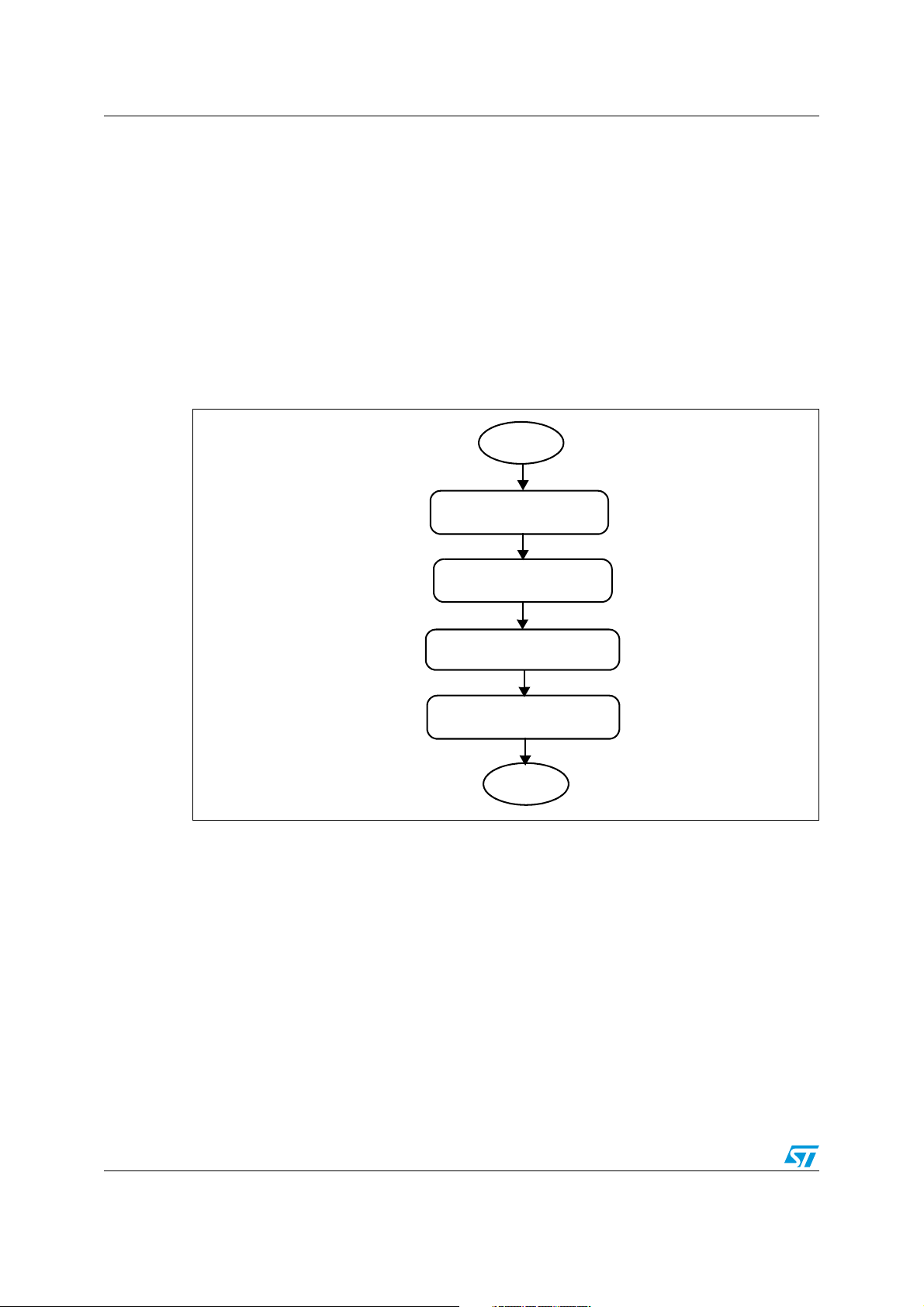
2.1.1 I2C initialization
To use ST7 I2C for PMBus communication, the peripheral is initialized for 100 kHz
communication speed. The I
2
C is configured with an address of 0x30, as it can act as a
slave due to its multi-master capability. The following flowchart shows the sequence.
Figure 2. Flowchart: I
2
C initialization
Initialize I
OAR1 and OAR2 registers
Configure slave addresses
Enable I
acknowledge in I2CCR register
Set communication speed as
100kHz in I2CCCR register
START
2
C CR, CCR,
in OAR1 and OAR2
2
C peripheral and
STOP
The above flowchart is implemented in the function PMBus_Init.
2.1.2 Slave address and command code
The PMBus master addresses the slave with a 7-bit address. Once the slave device
acknowledges the address, the command code is sent corresponding to the PMBus
command and SMBus protocol (refer to Section 3.1).
Then, the microcontroller decodes the command code as shown in the following sequence.
Simultaneously, the SMBus_Mode variable is updated.
8/43 Doc ID 13286 Rev 2
Page 9
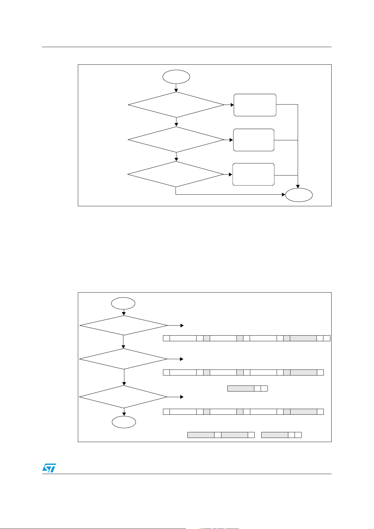
AN2511 Implementation of PMBus using ST7 I2C
Figure 3. Flowchart: data length calculation
START
Check if command code equal
to Block protocol
No
Check if command code equal
to Byte protocol
Ye s
Ye s
Update
SMBus_Mode
for Block Command
Byte Count=1,
Update
SMBus_Mode
for Byte Command
Byte Count=6,
No
Byte Count=2,
Check if command code equal
to word protocol
No
Ye s
Update
SMBus_Mode
for Word Command
STOP
Inside both PMBus_CommandRead and PMBus_CommandWrite functions,
PMBus_DataLengthCalc is called which calculates the data length based on the
command code received.
2.1.3 Read and write operation
PMBus master performs read/ write operations with the slave device. Depending on the
command code, either PMBus_CommandRead or PMBus_CommandWrite is called. Inside
this function, the SMBus transaction type is selected as shown in the following sequence.
Figure 4. Flowchart: read operation
START
Check if SMBus_Mode for
Byte command
No
Check if SMBus_Mode for Word
command
No
Check if SMBus_Mode for
Send Block command
No
STOP
Ye s
SMBus Read byte protocol
1711811711811
S Slave Address Wr
Ye s
SMBus Read word protocol
171181171181
S Slave Address Wr
Ye s
SMBus Read block protocol
171181171181
S Slave Address Wr
A Command Code A S Slave Address Rd A Data Byte A P
A Comm and Code A S Slave Address Rd A Data Byte Low A ...
811
Data Byte High A P
A Com mand Code A Sr Slave Address Rd A Count Byte = 1 A ...
8181...811
Data Byte 1 A Data Byte 2 A ... Data Byte N A P
Doc ID 13286 Rev 2 9/43
Page 10
Implementation of PMBus using ST7 I2C AN2511
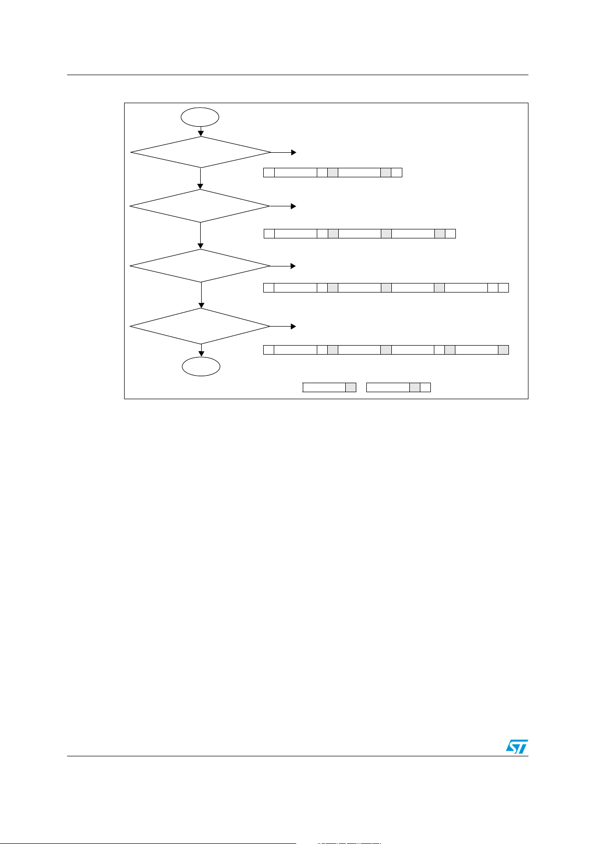
Figure 5. Flowchart: write operation
START
Check if SMBus_Mode for
Send Byte command
No
Check if SMBus_Mode for Write
Byte command
Check if SMBus_Mode for Write
Word command
No
Check if SMBus_Mode for
Write Block command
No
STOP
Ye s
SMBus Send byte protocol
1711811
S Slave Address Wr
Ye s
SMBus Write byte protocol
171181811
S Slave Address Wr
Ye s
SMBus Write word protocol
17118181811
S Slave Address Wr
Ye s
SMBus Write block protocol
17118181181
S Slave Address Wr
A Data Byte AP
A Comma nd Code A Data Byte AP
A Comma nd Code A Data Byte Low A Dat a Byte HIgh A P
A Command Co de A Byte Count = N Rd A Data Byte 1 A ...
81...811
Data Byte 2
A ... Data Byte N AP
During the PMBus communication, if there are any errors in communication (acknowledge
2
failure, arbitration loss, bus error or SMBus timeout), the I
C peripheral is disabled. It is re-
initialized again inside the PMBus write/ read functions.
In case the SMBus Alert pin is pulled low by the slave to inform the master that it wants to
communicate, the slave address is programmed with the alert response address (0x18).
This is acknowledged by the slave that alerted the master. After the communication between
the master and slave is complete, the slave address is programmed with the user-defined
slave address. The default value of this user-defined address is 0x30.
In case of group operation, the write operation flowchart is followed without the stop
condition.
10/43 Doc ID 13286 Rev 2
Page 11
AN2511 PMBus commands and source code
3 PMBus commands and source code
3.1 PMBus commands
The Part II - command language document of PMBus™ Power System Management
Protocol Specification v1.0 provides the list of PMBus commands. This driver supports the
following list of commands. For each command a table is given.
Table 1. Operation
Command name OPERATION
Command code 01h
The OPERATION command is used to turn the
Description
SMBus transaction type Read/ Write byte
Number of data bytes 1
Table 2. ON_OFF_CONFIG
Command name ON_OFF_CONFIG
Command code 02h
unit on and off in conjunction with the input from
the CONTROL (OUTEN) pin.
The ON_OFF_CONFIG command configures the
Description
combination of CONTROL (OUTEN) pin input
and serial bus commands needed to turn the unit
on and off.
SMBus transaction type Read/ Write byte
Number of data bytes 1
Table 3. CLEAR_FAULTS
Command name CLEAR_FAULTS
Command code 03h
Description
CLEAR_FAULTS is used to clear any fault bits
that have been set.
SMBus transaction type Send byte
Number of data bytes 0
Doc ID 13286 Rev 2 11/43
Page 12

PMBus commands and source code AN2511
Table 4. RESTORE_DEFAULT_ALL
Command name RESTORE_DEFAULT_ALL
Command code 12h
The RESTORE_DEFAULT_ALL command
instructs the PMBus device to copy the entire
contents of the non-volatile default store memory
Description
SMBus transaction type Send byte
Number of data bytes 0
Table 5. STORE_USER_ALL
Command name STORE_USER_ALL
Command code 15h
Description
SMBus transaction type Send byte
to the matching locations in the operating
memory. Any items in default store that do not
have matching locations in the operating memory
are ignored.
The STORE_USER_ALL command instructs the
PMBus device to copy the entire contents of the
operating memory to the matching locations in
the non-volatile user store memory. Any items in
operating memory that do not have matching
locations in the user store are ignored.
Number of data bytes 0
Table 6. VOUT_MODE
Command name VOUT_MODE
Command code 20h
VOUT_MODE command, used for commanding
and reading output voltage, consists of a three bit
Description
mode (only linear format is supported.) and a
five-bit parameter representing the exponent
used in output voltage Read/Writes.
SMBus transaction type Read/ Write byte
Number of data bytes 1
12/43 Doc ID 13286 Rev 2
Page 13

AN2511 PMBus commands and source code
Table 7. VOUT_COMMAND
Command name VOUT_COMMAND
Command code 21h
Description
SMBus transaction type Read/ Write word
Number of data bytes 2
Table 8. VOUT_MAX
Command name VOUT_MAX
Command code 24h
Description
SMBus transaction type Read/ Write word
Number of data bytes 2
Table 9. VOUT_MARGIN_HIGH
Command name VOUT_MARGIN_HIGH
Command code 25h
Description
VOUT_COMMAND is used to set the output
voltage, in volts (linear format).
The VOUT_ MAX command sets an upper limit
on the output voltage the unit can command
regardless of any other commands or
combinations.
This VOUT_MARGIN_HIGH command loads the
unit with the voltage to which the output is to be
changed when the OPERATION command is set
to "Margin High".
SMBus transaction type Read/ Write word
Number of data bytes 2
Table 10. VOUT_MARGIN_LOW
Command name VOUT_MARGIN_LOW
Command code 26h
This VOUT_MARGIN_LOW command loads the
Description
unit with the voltage to which the output is to be
changed when the OPERATION command is set
to "Margin Low".
SMBus transaction type Read/ Write word
Number of data bytes 2
Table 11. VOUT_OV_WARN_LIMIT
Command name VOUT_OV_WARN_LIMIT
Command code 42h
Doc ID 13286 Rev 2 13/43
Page 14

PMBus commands and source code AN2511
Table 11. VOUT_OV_WARN_LIMIT (continued)
The VOUT_OV_WARN_LIMIT command sets the
value of the output voltage at the sense or output
Description
SMBus transaction type Read/ Write word
Number of data bytes 2
Table 12. VOUT_UV_WARN_LIMIT
Command name VOUT_UV_WARN_LIMIT
Command code 43h
Description
SMBus transaction type Read/ Write word
Number of data bytes 2
Table 13. IOUT_OC_FAULT_LIMIT
Command name IOUT_OC_FAULT_LIMIT
pins that causes an output voltage high warning.
This value is typically less than the output
overvoltage threshold.
The VOUT_UV_WARN_LIMIT command sets the
value of the output voltage at the sense or output
pins that causes an output voltage low warning.
This value is typically greater than the output
undervoltage fault threshold
Command code 46h
The IOUT_OC_FAULT_LIMIT command sets the
Description
value of the sense output current, in amps (literal
format), that causes an overcurrent fault.
SMBus transaction type Read/ Write word
Number of data bytes 2
Table 14. IOUT_OC_WARN_LIMIT
Command name IOUT_OC_WARN_LIMIT
Command code 4Ah
The IOUT_OV_WARN_LIMIT command sets the
Description
SMBus transaction type Read/ Write word
Number of data bytes 2
Table 15. OT_FAULT_LIMIT
Command name OT_FAULT_LIMIT
Command code 4Fh
Description
value of the output current that causes an output
overcurrent warning.
The OT_FAULT_LIMIT command sets the value
of the sense temperature, in °C (literal format),
that causes an overtemperature fault
14/43 Doc ID 13286 Rev 2
Page 15

AN2511 PMBus commands and source code
Table 15. OT_FAULT_LIMIT (continued)
SMBus transaction type Read/ Write word
Number of data bytes 2
Table 16. OT_FAULT_RESPONSE
Command name OT_FAULT_RESPONSE
Command code 50h
The OT_FAULT_RESPONSE command instructs
Description
SMBus transaction type Read/ Write byte
Number of data bytes 1
Table 17. OT_WARN_LIMIT
Command name OT_WARN_LIMIT
Command code 51h
Description
the device on what action to take in response to
an overtemperature fault.
The OT_WARN_LIMIT command sets the value
of the sense temperature, in °C (literal format),
that causes an overtemperature warning.
SMBus transaction type Read/ Write word
Number of data bytes 2
Table 18. TON_DELAY
Command name TON_DELAY
Command code 60h
The TON_DELAY sets the time, in ms, from when
Description
a start condition is received (CONTROL signal
asserted and a valid OPERATION command
received) until the output voltage starts to rise.
SMBus transaction type Read/ Write word
Number of data bytes 2
Table 19. TON_RISE
Command name TON_RISE
Command code 61h
The TON_RISE sets the time, in ms, from when
Description
the output starts to rise until the voltage has
entered the regulation band.
SMBus transaction type Read/ Write word
Number of data bytes 2
Table 20. TOFF_DELAY
Command name TOFF_DELAY
Command code 64h
Doc ID 13286 Rev 2 15/43
Page 16

PMBus commands and source code AN2511
Table 20. TOFF_DELAY (continued)
The TOFF_DELAY sets the time, in ms, from
when a stop condition is received (CONTROL
Description
SMBus transaction type Read/ Write word
Number of data bytes 2
Table 21. TOFF_FALL
Command name TOFF_FALL
Command code 65h
Description
SMBus transaction type Read/ Write word
Number of data bytes 2
Table 22. STATUS_BYTE
Command name STATUS_BYTE
Command code 78h
Description
SMBus transaction type Read byte
signal negated or a valid OPERATION command
received) until the unit stops transferring energy
to the output.
The TOFF_FALL sets the time, in ms, from the
end of the turnoff delay time until the voltage is
commanded to zero. Note that this command can
only be used with a device whose output can sink
enough current to cause the output voltage to
decrease at a controlled rate.
The STATUS_BYTE command returns one byte
of information with a summary of the most critical
faults
Number of data bytes 1
Table 23. STATUS_WORD
Command name STATUS_WORD
Command code 79h
The STATUS_WORD command returns two
Description
bytes of information with a summary of the units
fault condition.
SMBus transaction type Read word
Number of data bytes 2
:
Table 24. STATUS_VOUT
Command name STATUS_VOUT
Command code 7Ah
Description
The STATUS_VOUT commands returns one byte
with status information on Vout.
16/43 Doc ID 13286 Rev 2
Page 17

AN2511 PMBus commands and source code
Table 24. STATUS_VOUT (continued)
SMBus transaction type Read byte
Number of data bytes 1
Table 25. STATUS_IOUT
Command name STATUS_IOUT
Command code 7Bh
Description
SMBus transaction type Read byte
Number of data bytes 1
Table 26. STATUS_TEMPERATURE
Command name STATUS_TEMPERATURE
Command code 7Dh
Description
SMBus transaction type Read byte
Number of data bytes 1
STATUS_IOUT commands returns one byte with
status information on Iout.
STATUS_TEMPERATURE commands returns
one byte with status information on temperature.
Doc ID 13286 Rev 2 17/43
Page 18

PMBus commands and source code AN2511
Table 27. STATUS_MFR_SPECIFIC
Command name STATUS_MFR_SPECIFIC
Command code 80h
STATUS_MFR_SPECIFIC commands returns
Description
SMBus transaction type Read byte
Number of data bytes 1
Table 28. READ_VOUT
Command name READ_VOUT
Command code 8Bh
Description
SMBus transaction type Read word
Number of data bytes 2
Table 29. READ_IOUT
Command name READ_IOUT
Command code 8Ch
Description
SMBus transaction type Read word
Number of data bytes 2
Table 30. READ_TEMPERATURE
Command name READ_TEMPERATURE
Command code 8Dh
Description
SMBus transaction type Read word
Number of data bytes 2
one byte with the manufacturer specific status
information.
The READ_VOUT command returns the actual
measured output voltage in the same format as
set by the VOUT_MODE command.
The READ_IOUT command returns the
measured output current in amperes.
Up to three temperature readings can be
returned for each device.
18/43 Doc ID 13286 Rev 2
Page 19

AN2511 PMBus commands and source code
Table 31. PMBUS_REVISION
Command name PMBUS_REVISION
Command code 98h
PMBUS_REVISION command stores or reads
Description
SMBus transaction type Read byte
Number of data bytes 1
Table 32. MFR_ID
Command name MFR_ID
Command code 99h
Description
SMBus transaction type Read/Write block
Number of data bytes 7
Table 33. MFR_MODEL
Command name MFR_MODEL
the revision of the PMBus to which the device is
compliant.
The MFR_ID commands loads the unit with
ASCII characters that contain the manufacturer's
ID (name, abbreviation or symbol that identifies
the unit's manufacturer). This is typically only
done once at the time of manufacture.
Command code 9Ah
The MFR_MODEL command loads the unit with
Description
ASCII characters that contain the manufacturer's
model number. This is typically done once at the
time of manufacture.
SMBus transaction type Read/Write block
Number of data bytes 6
Table 34. MFR_REVISION
Command name MFR_REVISION
Command code 9Bh
The MFR_REVISION command loads the unit
Description
with ASCII characters that contain the
manufacturer's revision number. This is typically
done once at the time of manufacture.
SMBus transaction type Read/Write block
Number of data bytes 2
Doc ID 13286 Rev 2 19/43
Page 20

PMBus commands and source code AN2511
Table 35. MFR_LOCATION
Command name MFR_LOCATION
Command code 9Ch
The MFR_REVISION command loads the unit
Description
SMBus transaction type Read/Write block
Number of data bytes 2
Table 36. MFR_DATE
Command name MFR_DATE
Command code 9Dh
Description
SMBus transaction type Read/Write block
Number of data bytes 6
Table 37. MFR_SERIAL
Command name MFR_SERIAL
with ASCII characters that contain the
manufacturer's revision number. This is typically
done once at the time of manufacture.
The MFR_DATE command loads the unit with
ASCII characters that identify the unit's date of
manufacture. This is typically done once at the
time of manufacture.
Command code 9Eh
Description
The MFR_SERIAL command loads the unit with
a serial number to uniquely identify the unit
SMBus transaction type Read/Write block
Number of data bytes 6
Table 38. MFR_SPECIFIC_00
Command name MFR_SPECIFIC_00
Command code D0h
Description
The MFR_SPECIFIC_00 command provides
access control for NVM register writes.
SMBus transaction type Read byte
Number of data bytes 1
20/43 Doc ID 13286 Rev 2
Page 21

AN2511 PMBus commands and source code
Table 39. MFR_SPECIFIC_01
Command name MFR_SPECIFIC_01
Command code D1h
Description
The MFR_SPECIFIC_01 command provides
access control for configuration register writes.
SMBus transaction type Read byte
Number of data bytes 1
Table 40. MFR_SPECIFIC_02
Command name MFR_SPECIFIC_02
Command code D2h
Description
The MFR_SPECIFIC_02 is a manufacturer
defined command.
SMBus transaction type Read byte
Number of data bytes 1
3.2 Source code
The source code is attached in the zip file along with the application note. This source code
is organized as shown below.
' Workspace directory
' Debug
' object files, list files, map files, executable files (.elf), hex code
(.s19)
' Sources
' Main.c: Contains main source code. In this file, PMBus interface functions
are called (refer to section 3.3).
' Main.h: Contains prototype of all functions used in Main.c.
' PMBus.c: Contains functions for PMBus write and read operation. The data
length calculator function and I2C and Alert signal interrupt sub-
routines are also written inside this file.
' PMBus.h: Contains prototype of all functions and enumerated data
' SMBus_Master.c: Contains source code for differnet SMBus master
' SMBus_Master.h: Contains prototype of all functions and enumerated data
' st72264g1.h: Contains register mapping for ST72F264G1 device.
' ST7_hr.h: Contains hardware register bit definitions for ST7 MCU
' ST7_Config.h: Contains compiler selection, peripheral register inclusion,
' interrupt_vector.c: Contains general Interrupt vector table for ST7 devices
types used in PMBus.c.
transaction bus protocols.
types used in SMBus_Master.c.
header files inclusion for linking, macros for assembly instructions
and Fcpu Definition.
Doc ID 13286 Rev 2 21/43
Page 22

PMBus commands and source code AN2511
3.3 Example
This section explains how to use the PMBus driver. An example operation of write/ read
commands are shown.
/*****************************************************************************
COPYRIGHT 2005 STMicroelectronics
Source File Name : Main.c
Group : IMS Systems Lab
Author : Telecom Team
Date First Issued: 01/09/2006
-*-*-*-*-*-*-*-*-*-*-*-*-*-*-*-*-*-*-*-*-*-*-*-*-*-*-*-*-*-*-*-*-*-*-*-*-*-*-*-
THE SOFTWARE INCLUDED IN THIS FILE IS FOR GUIDANCE ONLY. STMicroelectronics
SHALL NOT BE HELD LIABLE FOR ANY DIRECT, INDIRECT OR CONSEQUENTIAL
DAMAGES WITH RESPECT TO ANY CLAIMS ARISING FROM USE OF THIS SOFTWARE.
-*-*-*-*-*-*-*-*-*-*-*-*-*-*-*-*-*-*-*-*-*-*-*-*-*-*-*-*-*-*-*-*-*-*-*-*-*-*-*********************************Documentation**********************************
General Purpose - Contains main source code. In this file, the PMBus command files
are written.
******************************************************************************/
#include "ST7_config.h" /* Fcpu defined as 8MHz */
#include "main.h" /* Contains the global variables used in main.c */
#include "ST7_hr.h" /* Contains the register and flags for ST7 */
extern volatile unsigned int SMB_TimeCount; /* Time count variable */
#pragma space extern [] @tiny /* To force following variables into short
addressing memory */
extern unsigned char Data_Buff [32] ; /* Buffer to store data */
/* Variables to differentiate the different SMBus transaction types */
extern volatile unsigned char SMBus_Mode ;
extern volatile unsigned char SMB_Err_Status ; /* Error status */
/* Master to address slave with this
address */
static volatile unsigned char PMBus_SlaveAdd = 0x80;
/* Master to address slave with this
address */
static volatile unsigned char PMBus_SlaveAdd = 0x80;
/*----------------------------------------------------------------------------ROUTINE NAME : Main
INPUT : None
OUTPUT : None
DESCRIPTION : Using this file, user can write/ read PMBus commands.
COMMENTS : Programs jumpts into this routine when microcontroller is reset
-----------------------------------------------------------------------------*/
void main()
{
unsigned char temp ;
SMBs_Address_t PMBus_Err ; /* To check errors in PMBus communication */
/*----------------------- Port A configuration ----------------------------*/
PADDR &= (unsigned char)~PORTA_DEFAULT;
PADDR = PORTA_DEFAULT ; /* Other pins configured as floating input */
PAOR = (unsigned char)(PORTA_DEFAULT) ;
/*----------------------- Port C configuration ----------------------------*/
PCDDR = CONTROL ; /* PC0 floating input, others push pull output */
22/43 Doc ID 13286 Rev 2
Page 23

AN2511 PMBus commands and source code
PCOR = CONTROL ;
PCDR = CONTROL ;
/*----------------------- Alert Interrupt configuration ---------------------
----------*/
EnableInterrupts; /* Resets interrupt mask */
MISCR1 = 0x10 ; /* EI0 on falling edge low level for Alert interrupt */
/*---------------------PMBus communication configuration-------------------*/
while (1)
{
/* I2C configuration: ST7 I2C address 0x30, communication speed 100kHz */
PMBus_Init (SMBs_MISC, SLAVEADD, 0x40, 0x23);
/* Checking if an alert signal is received from slave */
if (SMBus_Mode & SMB_ARA)
{
/* ST7 I2C sends the alert response address to check which slave
alerted */
PMBus_Err = SMBm_ReceiveByte (ALERTRESPONSEADD, Data_Buff);
/* Alerted slave address will be used for any further communication */
PMBus_SlaveAdd = *Data_Buff ;
SMBus_Mode &= (unsigned char) ~SMB_ARA ;
}
Command_Code = 0x01; /* User should enter the PMBus command code here */
PMBus_CommandWrite (Command_Code); /* Writes data from Data_Buff */
Command_Code = 0x02; /* User should enter the PMBus command code here */
PMBus_CommandRead (Command_Code);
if (SMB_Err_Status)
{ /* I2C status register read to clear any
errors */
SMB_Err_Status = I2CSR2 ;
SMB_Err_Status = 0 ;
}
} /* End of while (1) */
} /* End of main */
3.4 Limitations
1. The SMBus driver used in this application note is tested only for write word, read word
and write block protocols with PEC disabled.
2. The SMBus driver doesn't meet the clock low extending feature of SMBus v1.1 due to
the limitation of the I
3. In case of PEC, when slave is acting as receiver, the ACK bit is not disabled if the PEC
received from master transmitter is different from slave. It is stored in the user address
as the last byte. It is the responsibility of the user to check the master PEC with the
slave PEC to decide on data validity.
/* Read data and store it in Data_Buff */
2
C peripheral.
Doc ID 13286 Rev 2 23/43
Page 24

PMBus interfacing results AN2511
4 PMBus interfacing results
This section describes the results of interfacing the demonstration board with Artesyn and
SiLabs modules.
4.1 Interfacing with Artesyn module
The following table shows the different PMBus commands and ST demonstration board
results compared to the Artesyn DPL20C PMbus module.
Table 41. PMBus interfacing with Artesyn module: results
Command
code
01 OPERATION Read/ write byte 1 80 80
02 ON_OFF_CONFIG Read/ write byte 1 14 14
03 CLEAR_FAULTS Send byte 0
12
15 STORE_USER_ALL Send byte 0
20 VOUT_MODE Read/ write byte 1 1 A 1 A
21 VOUT_COMMAND Read/ write word 2 00 60 00 60
24 VOUT_MAX Read/ write word 2 01 60 01 60
25 VOUT_MARGIN_HIGH Read/ write word 2 00 6 A 00 6 A
26 VOUT_MARGIN_LOW Read/ write word 2 00 56 00 56
42
43
46
4A
PMBus command
RESTORE_DEFAULT_
ALL
VOUT_OV_WARN_LIM
IT
VOUT_UV_WARN_LIM
IT
IOUT_OC_FAULT_LI
MIT
IOUT_OC_WARN_LIM
IT
SMBus transaction
type
Send byte 0
Read/ write word 2 00 6E 00 6E
Read/ write word 2 00 56 00 56
Read/ write word 2 00 19 00 19
Read/ write word 2 00 17 00 17
Number
of data
bytes
Data
(Si8250)
Data
(ST7)
4F OT_FAULT_LIMIT Read/ write word 2 00 78 00 78
50
51 OT_WARN_LIMIT Read/ write word 2 00 6E 00 6E
60 TON_DELAY Read/ write word 2 00 00 00 00
61 TON_RISE Read/ write word 2 00 0A 00 0A
64 TOFF_DELAY Read/ write word 2 00 00 00 00
65 TOFF_FALL Read/ write word 2 00 00 00 00
24/43 Doc ID 13286 Rev 2
OT_FAULT_RESPONS
E
Read/ write byte 1 B1 B1
Page 25

AN2511 PMBus interfacing results
Table 41. PMBus interfacing with Artesyn module: results (continued)
Command
code
78 STATUS_BYTE Read byte 1 41 41
79 STATUS_WORD Read word 2 00 41 00 41
7A STATUS_VOUT Read byte 1 00 00
7B STATUS_IOUT Read byte 1 00 00
7D
80
8B READ_VOUT Read word 2 00 01 00 01
8C READ_IOUT Read word 2 D7 C3 D7 C3
8D READ_TEMPERATURE Read word 2 00 20 00 1D
98 PMBUS_REVISION Read byte 1 01 01
99 MFR_ID Read block 7
9A MFR_MODEL Read block 6
9B MFR_REVISION Read/ write block 2 31 02 31 41
9C MFR_LOCATION Read/ write block 2 5A 02 5A 53
PMBus command
STATUS_TEMPERATU
RE
STATUS_MFR_SPECI
FIC
SMBus transaction
type
Read byte 1 00 00
Read byte 1 02 02
Number
of data
bytes
Data
(Si8250)
41 52 54 45
53 59 4E
44 50 4C 32
30 43
Data
(ST7)
41 52 54
45 53 59
4E
44 50 4C
32 30 43
9D MFR_DATE Read/ write block 6
9E MFR_SERIAL Read/ write block 6
D0 MFR_SPECIFIC_00 Read byte 1 28 28
D1 MFR_SPECIFIC_01 Read byte 1 10 10
D2 MFR_SPECIFIC_02 Read byte 1 0A 0A
4.2 Interfacing with SiLabs module
The following table shows the different PMBus commands and ST demonstration board
results compared to Silicon Labs Si8250 - TB module.
Table 42. PMBus interfacing with SiLabs module: results
Command
code
01 OPERATION Read/ write byte 1 C0 C0
02 ON_OFF_CONFIG Read/ write byte 1 1E 1E
PMBus command
SMBus transaction
type
Number
of data
bytes
32 34 30 33
36 06
31 32 33 34
35 06
Data
(Si8250)
32 34 30
33 36 36
31 32 33
34 35 36
Data
(ST7)
Doc ID 13286 Rev 2 25/43
Page 26

PMBus interfacing results AN2511
Table 42. PMBus interfacing with SiLabs module: results (continued)
Command
code
03 CLEAR_FAULTS Send byte 0
12 RESTORE_DEFAULT_ALL Send byte 0
15 STORE_USER_ALL Send byte 0
20 VOUT_MODE Read/ write byte 1 11 11
21 VOUT_COMMAND Read/ write word 2 7F F6 7F F6
24 VOUT_MAX Read/ write word 2 89 94 89 94
25 VOUT_MARGIN_HIGH Read/ write word 2 00 6A 00 6A
25 VOUT_MARGIN_HIGH Read/ write word 2 86 5C 86 5C
26 VOUT_MARGIN_LOW Read/ write word 2 79 90 79 90
42 VOUT_OV_WARN_LIMIT Read/ write word 2 89 94 89 94
43 VOUT_UV_WARN_LIMIT Read/ write word 2 76 58 76 58
4F OT_FAULT_LIMIT Read/ write word 2 EB 20 EB 20
50 OT_FAULT_RESPONSE Read/ write byte 1 00 00
51 OT_WARN_LIMIT Read/ write word 2 EA D0 EA D0
60 TON_DELAY Read/ write word 2 00 0A 00 0A
61 TON_RISE Read/ write word 2 00 32 00 32
PMBus command
SMBus transaction
type
Number
of data
bytes
Data
(Si8250)
Data
(ST7)
64 TOFF_DELAY Read/ write word 2 00 0A 00 0A
65 TOFF_FALL Read/ write word 2 00 C8 00 C8
78 STATUS_BYTE Read byte 1 04 04
79 STATUS_WORD Read word 2 00 04 00 04
7A STATUS_VOUT Read byte 1 00 00
7B STATUS_IOUT Read byte 1 00 00
7D STATUS_TEMPERATURE Read byte 1 20 20
80 STATUS_MFR_SPECIFIC Read byte 1 00 00
8B READ_VOUT Read word 2 80 4E 80 76
8C READ_IOUT Read word 2 D7 C3 00 00
8D READ_TEMPERATURE Read word 2 EF 56 EF 56
98 PMBUS_REVISION Read byte 1 00 00
D0 MFR_SPECIFIC_00 Read byte 1 67 67
D1 MFR_SPECIFIC_01 Read byte 1 EF EF
D2 MFR_SPECIFIC_02 Read byte 1 08 08
26/43 Doc ID 13286 Rev 2
Page 27

AN2511 PMBus demonstration board
5 PMBus demonstration board
To show the features of the ST7 I2C working as a PMBus, a demonstration board is
available on request. Please contact the nearest ST office to get this board. The evaluation
board has an ST72F264G1 MCU that has 4 KBytes Flash memory. All PMBus
functionalities are not shown, as this evaluation board has hyperterminal interface which
requires lot of messages to be stored in program memory.
5.1 System requirements
In order to use the PMBus demonstration board with the Windows operating system. The
PC should support hyperterminal software and RS232 communication using DB9
connector.
5.2 Software setup
To configure the PC hyperterminal software, the user should follow the steps as mentioned
below.
1. Click on Start -> Programs -> Accessories -> Communications -> HyperTerminal
as shown below.
Figure 6. PC hyperterminal application
2. Select the correct port in which RS232 (9-pin cable) is connected (refer to Section 3).
3. Configure the following baud rate (bits per second) in hyperterminal: File -> Properties
-> Connect to -> Configure. If the user configures any baud rate other than 38400,
then RS232 communication fails.
Doc ID 13286 Rev 2 27/43
Page 28

PMBus demonstration board AN2511
Figure 7. Baud rate configuration
4. Configure the following settings in hyperterminal: File -> Properties -> Settings ->
ASCII setup
Figure 8. Hyperterminal settings - ASCII setup configuration
5. Press call in hyperterminal to establish a connection with the board.
5.3 Hardware setup
To configure the hardware board, the user should follow these steps:
1. Jumper settings: There are four jumpers (JP1, JP2, JP3 and JP4) available on the
board. The detail of these connectors is as follows:
a) JP1: JP1 pins should be connected using the jumper if there is no pull-up
connected in the clock line of the I
pulled up with a resistor value of 4.7 kΩ.
b) JP2: JP2 pins should be connected using the jumper if there is no pull-up
connected in the data line of the I
pulled up with a resistor value of 4.7 kΩ.
c) JP3: JP3 is used to select the clock source for the ST7 microcontroller. From the
JP3 side, if the jumper is connected between pins 1 and 2 then the application
28/43 Doc ID 13286 Rev 2
2
C bus. Once connected, the I2C clock line is
2
C bus. Once connected, the I2C data line is
Page 29

AN2511 PMBus demonstration board
runs using the resonator clock (16 MHz). If the jumper is connected between pins
2 and 3 then the application is stopped and ST7 MCU can be re-programmed.
d) JP4: JP4 is used to select the power supply as described below. From the JP4
side, if the jumper is connected between pins 2 and 3 then the application runs
using the direct supply given from `POWER' connector. If the jumper is connected
between pins 1 and 2 then the application runs using the DC adapter supply given
from J1.
2. Power settings: The demonstration board can be powered by one of the following
options:
a) DC adapter: Connect a DC adapter to J1. The DC adapter should supply a
minimum of 7 V and maximum of 18 V, 1 A. This supply is regulated to 5 V supply
using an L7805 regulator.
b) Regulated supply: The user can use a direct 3 V to 5 V supply. The supply and
Gnd points should be connected to the `POWER' connector pins 1 and 2. Here,
`POWER' connector pin 1 is referred from the JP4 jumper side (from the right
side).
Doc ID 13286 Rev 2 29/43
Page 30

Using the demonstration board AN2511
6 Using the demonstration board
After installing the setup as explained in Section 1, the following message appears in
hyperterminal.
Figure 9. Hyperterminal message to show company name and selection of
communication speed
If there is any problem in getting the message, press the switch provided in the
demonstration board. This switch re-starts the application.
6.1 Normal operation
The following sections explain how to initiate PMBus communication and how to read/ write
PMBus commands with hyperterminal.
6.1.1 Selection of communication speed
After the message appears as shown in Figure 9, the user should enter 1 or 2 to select the
PMBus communication speed as 100 kHz or 400 kHz respectively. The default speed value
selected is 100 kHz.
If the user enters any other value other than 1 and 2, the previous speed value is retained.
6.1.2 Selection of packet error checking
After the message appears as shown in Figure 10, the user should enter 1 or 2 to enable
PEC and disable PEC respectively. If PEC is enabled, all address, command code and data
communications are checked through CRC-8 check. The default PEC value is PEC
disabled.
If the user enters any other value other than 1 and 2, the previous speed value is retained.
Figure 10. PEC selection
6.1.3 Selection of slave address
The user should enter the slave address of the PMBus device. The slave address should be
in hexadecimal format. The slave addresses of different competitor’s module are given
below. Artesyn DPL20C module: 0x30 SiLabs Si8250-TB module : 0x80.
The slave address could change from one device to another device. The user must refer to
the product datasheet and development kit documents to decide on the slave address. An
example entry of slave address with Artesyn DPL20C module is shown below.
30/43 Doc ID 13286 Rev 2
Page 31

AN2511 Using the demonstration board
Figure 11. Slave address entry message
If the user enters a wrong slave address then one of the following error messages shown in
Figure 12 or Figure 13 appears.
Figure 12. Wrong slave address entry - response 1
Figure 13. Wrong slave address entry - response 2
6.1.4 Selection of read/write mode
Data can be written into or data can be read back from the PMBus salve device connected.
The following figure provides the key option to select one of the modes.
Figure 14. Options to select read/ write mode
6.1.5 Single read mode
The user can press 1 to select read mode. Then the user can enter any command code with
reference to Section 3 to read byte/ word/ block of data. An example of this is shown below.
Figure 15. Single read operation
Doc ID 13286 Rev 2 31/43
Page 32

Using the demonstration board AN2511
6.1.6 Continuous read mode
The user can press 0 to read all PMBus commands. The lists of supported commands are
shown in the following figure.
Figure 16. Continuous read operation
Command codes 0xD0, 0xD1 and 0xD2 are not supported in continuous read mode. If the
user wants to read these commands, they can be read by using single read mode.
6.1.7 Write mode
The user can press 2 to select write mode. After the following figure appears, the user can
enter any command code with reference to Section 2.1 on page 8 to write byte/ word/ block
of data.
Figure 17. Write mode command code entry message from hyperterminal
Then the user can enter any command code with reference to Section 4 to write byte/ word/
block of data. The user can enter data after the following message.
Figure 18. Write mode data entry message from hyperterminal
Data should be entered in hex format. If the user wants to enter date/ serial numbers, they
should be entered in ASCII format.
32/43 Doc ID 13286 Rev 2
Page 33

AN2511 Using the demonstration board
For example, to enter a date as “15 -12-1991”, then data should be entered as
313531323931 (where 31h=ASCII ”1”, 35h=ASCII “5”, etc., and the date will read “151291”).
An example of this operation is shown below.
Figure 19. Write mode operation example
When reading back the date written using single read commands, the following message is
displayed:
Figure 20. Read operation to check data writing
6.1.8 Group command
The user can press 3 to select group command mode. In this demonstration board, the user
can write multiple commands for multiple slave addresses.
After Figure 21 appears, the user can enter any command code and data with reference to
Section 3.1: PMBus commands to write byte/ word/ block of data. The user can enter 5
commands and data for the group command. If the user wants to write less than 5
commands, the user can press * to terminate the group command operation.
Doc ID 13286 Rev 2 33/43
Page 34

Using the demonstration board AN2511
Figure 21. Group command code entry message from hyperterminal
An example of this operation is shown below.
Figure 22. Group command operation example
6.2 Error conditions
The following error conditions may be encountered during PMBus communication.
6.2.1 Invalid command code
If the user enters a command code that is not available in the list or enters an incorrect
option to select read/write options, the following error message appears:
Figure 23. Invalid command message
An example is shown in Figure 24.
34/43 Doc ID 13286 Rev 2
Page 35

AN2511 Using the demonstration board
Figure 24. Example of invalid command
6.2.2 Communication timeout
This error appears when the PMBus communication fails due to one of the following
reasons:
● The slave device doesn’t acknowledge the master
● The clock low interval exceeds the value of TTIMEOUT,MIN as defined by (SMBus
Specification 1.1)
● TLOW:SEXT and TLOW:MEXT conditions are not met
● Bus error or arbitration errors in PMBus communication
In these conditions, the following error message appears:
Figure 25. Communication timeout message
Doc ID 13286 Rev 2 35/43
Page 36

Hardware description AN2511
7 Hardware description
This section provides schematics, BOM (bill of materials), layout and picture of the
demonstration board.
7.1 Schematic and layout
The following figures show the schematic and layouts of the demonstration board.
Figure 26. Demonstration board schematic
*
*0
&
N
#
6
)##3%,
633
6$$
*0
K
K
2
2
3#,
3$!
2
2
2
2
#/.42/,
0!
4$/
2$)
3-"?!,%24
0#
)##$!4!
)###,+
0!0!
0!
0!
)##3%,
0#
0#
0#
0#
2$)0!
3#,0!
3$!0!
4$/0!
23 ).4%2&!#%
6
2/54
2/54
4/54
4/54
2).
4).
2).
4).
5
2$)
4$/
-#5
)## #/.
#/.
#
2
2%3%4
)##3%,
)##$!4!
)###,+
6##
*0
&
N
#
2
K
3
#
330"
2%3%4/3#/3#
3#+0"-)3/0"-/3)0"
5
2%3%4
/3#).
0"
0"
/3#
/3#
0"
0"
N&
-(Z
9
#
PF
#
PF
0#
0"0"
0"
0"0#
0#
0"
0"
34&'-
0#
0#
0#
0"
0"
6
$
3-$ ,%$
2
2
40
#
U&V
6
N&
40
#
6 6## 6$$
0!
'.$
0"
/
'
,#$442
)
5
&
N
0"
*
#
&!5,4
*
6^6
*!#+
0"
0"
#/.
*
0/7%2
0"
0"
*
#/.
-5,4)0(!3%
-!.!'%-%.4
/0%2!4)/.3
#/.
3$!
3#,
3-"?!,%24
#/.42/,
*
0-"53
).4%2&!#%
#/.
2%3%4
40
#/.
3%4
2%
#
6##
#
#6
##6
#
U& 6
K
)##
/3#).
/3#
0#
0#
0#
*
$"
N&
'.$
34#42
#
U& 6
#
U& 6
U& 6
0#
0#
0"
0"
%84 ).4%2&!#%
!-V
6
#/.
36/43 Doc ID 13286 Rev 2
Page 37

AN2511 Hardware description
Figure 27. Top view layout of the demonstration board
Figure 28. Bottom view layout of the demonstration board
Doc ID 13286 Rev 2 37/43
Page 38

7.2 Bill of materials (BOM)
The following table shows the BOM of the demonstration board.
Table 43. Bill of material
Capacitors: C2, C3, C9, C10, C11, C12, C13 100 nF 805 Any
Doc ID 13286 Rev 2 38/43
Table 43:
Reference
Capacitors: C7, C8 10 nF 805 Any
Capacitors: C5, C6 10 pF 805 Any
Capacitors: C1 330 nF 805 Any
Polarized capacitor (Axial): C4 100 µF/ 10 V RB-5.5 Any
Resistors: R1, R2, R3 4.7 kΩ 805 Any
Resistors: R4, R5 100 Ω 805 Any
Resistors: R6 220 Ω 805 Any
Resistors: R7 10 kΩ 805 Any
Connector: TP3 CON1 SIP-1 Any
Value / g e neri c par t
number
Package Manufacturer
Manufacturer’s
ordering code /
orderable part
number
AN2511 Hardware description
Supplier
Connectors: J2, J3, J4, JP1, JP2, POWER CON2 SIP-2 Any
Connectors: JP3, JP4 CON3 SIP-3 Any
Connector: J5 CON4 SIP-4 Any
Connector J7 CON7 SIP-7 Any
9 pin female RS232 connector: J6 DB9 DB9/F GM (801-036)
Crystal: Y1 16 MHz (KDS) XTAL-1 Any
Header: CON1 ICC IDC-10B Any
Power Jack connector: J1 JACK TAP_2.5 mm GM: K375A
Regulator: U1 L7805CD2T-TR TO-220 STMicroelectronics L7805CD2T-TR
SMD LED: D1 SMD LED LED-SMD Faichild
Page 39

39/43 Doc ID 13286 Rev 2
Table 43. Bill of material (continued)
Reference
MCU U2 ST72F264G1M6 SOL-28 STMicroelectronics ST72F264G1M6
RS232 level translator: U3 ST3232CTR SO-16 STMicroelectronics ST3232CTR
Switch S1 TACT SWITCH PUSH-4 Any
Diode: D2 1N5817 DO41 STMicroelectronics
ZENER diode: ZD1 SMAJ TO220 STMicroelectronics
Value / g e neri c par t
number
Package Manufacturer
Manufacturer’s
ordering code /
orderable part
number
Hardware description AN2511
Supplier
Page 40

Hardware description AN2511
7.3 Demonstration board photo
The following figure shows the picture of the demonstration board.
Figure 29. STEVAL-ISQ002V1
40/43 Doc ID 13286 Rev 2
Page 41

AN2511 Configuration
Appendix A Configuration
A.1 RS232 configuration
The following figure shows the pin description of the RS232 D9 connector.
Figure 30. Pin description of RS232 D9 connector
Doc ID 13286 Rev 2 41/43
Page 42

Revision history AN2511
Revision history
Table 44. Document revision history
Date Revision Changes
17-Apr-2007 1 Initial release.
– Modified: Figure 9, 10, 16, 17, 18, 19, 20, 23, 24, 25, 26, 29,
25-Aug-2010 2
Ta bl e 4 3
– Added: Figure 27, 28
– Minor text changes
42/43 Doc ID 13286 Rev 2
Page 43

AN2511
Please Read Carefully:
Information in this document is provided solely in connection with ST products. STMicroelectronics NV and its subsidiaries (“ST”) reserve the
right to make changes, corrections, modifications or improvements, to this document, and the products and services described herein at any
time, without notice.
All ST products are sold pursuant to ST’s terms and conditions of sale.
Purchasers are solely responsible for the choice, selection and use of the ST products and services described herein, and ST assumes no
liability whatsoever relating to the choice, selection or use of the ST products and services described herein.
No license, express or implied, by estoppel or otherwise, to any intellectual property rights is granted under this document. If any part of this
document refers to any third party products or services it shall not be deemed a license grant by ST for the use of such third party products
or services, or any intellectual property contained therein or considered as a warranty covering the use in any manner whatsoever of such
third party products or services or any intellectual property contained therein.
UNLESS OTHERWISE SET FORTH IN ST’S TERMS AND CONDITIONS OF SALE ST DISCLAIMS ANY EXPRESS OR IMPLIED
WARRANTY WITH RESPECT TO THE USE AND/OR SALE OF ST PRODUCTS INCLUDING WITHOUT LIMITATION IMPLIED
WARRANTIES OF MERCHANTABILITY, FITNESS FOR A PARTICULAR PURPOSE (AND THEIR EQUIVALENTS UNDER THE LAWS
OF ANY JURISDICTION), OR INFRINGEMENT OF ANY PATENT, COPYRIGHT OR OTHER INTELLECTUAL PROPERTY RIGHT.
UNLESS EXPRESSLY APPROVED IN WRITING BY AN AUTHORIZED ST REPRESENTATIVE, ST PRODUCTS ARE NOT
RECOMMENDED, AUTHORIZED OR WARRANTED FOR USE IN MILITARY, AIR CRAFT, SPACE, LIFE SAVING, OR LIFE SUSTAINING
APPLICATIONS, NOR IN PRODUCTS OR SYSTEMS WHERE FAILURE OR MALFUNCTION MAY RESULT IN PERSONAL INJURY,
DEATH, OR SEVERE PROPERTY OR ENVIRONMENTAL DAMAGE. ST PRODUCTS WHICH ARE NOT SPECIFIED AS "AUTOMOTIVE
GRADE" MAY ONLY BE USED IN AUTOMOTIVE APPLICATIONS AT USER’S OWN RISK.
Resale of ST products with provisions different from the statements and/or technical features set forth in this document shall immediately void
any warranty granted by ST for the ST product or service described herein and shall not create or extend in any manner whatsoever, any
liability of ST.
ST and the ST logo are trademarks or registered trademarks of ST in various countries.
Information in this document supersedes and replaces all information previously supplied.
The ST logo is a registered trademark of STMicroelectronics. All other names are the property of their respective owners.
© 2010 STMicroelectronics - All rights reserved
STMicroelectronics group of companies
Australia - Belgium - Brazil - Canada - China - Czech Republic - Finland - France - Germany - Hong Kong - India - Israel - Italy - Japan -
Malaysia - Malta - Morocco - Philippines - Singapore - Spain - Sweden - Switzerland - United Kingdom - United States of America
www.st.com
Doc ID 13286 Rev 2 43/43
 Loading...