

Page 1

AN2510
Application note
Combo IC for PFC and ballast control
Introduction
A new control IC, the L6585D, has been designed to manage electronic ballasts for
fluorescent lamps. It includes both Power Factor Correction and half-bridge sections and
embeds a wide range of features to provide an energy saving and cost effective solution.
The high-voltage single chip approach optimizes the management of lamp critical conditions
such as the pre-heating and ignition of start up and fault and lamp replacement. The internal
logic, guided by precise internal references and timings, is able to carry out all of these
phases. The PFC section has superior performance in terms of harmonic content
mitigation. High Power Factor (PF) and Total Harmonic Distortion (THD) reduction are
obtained as required by international norms, especially concerning Universal input voltage
operations.
Particular care has been given to pre-heating and ignition phases prior to lamp start up in
order to ensure the proper filament warming up and extend lamp life.
Innovative circuitry allows an improved control of the lamp voltage during ignition as well as
protection against failures due to lamp aging.
The use of this new control IC simplifies the industrialization of electronic ballasts which
increases application reliability and reduces its dimensions and cost.
March 2007 Rev 1 1/22
www.st.com
Page 2

Contents AN2510
Contents
1 L6585 Integrated circuit . . . . . . . . . . . . . . . . . . . . . . . . . . . . . . . . . . . . . . 4
2 Device blocks description . . . . . . . . . . . . . . . . . . . . . . . . . . . . . . . . . . . . 5
2.1 Start-up and shutdown . . . . . . . . . . . . . . . . . . . . . . . . . . . . . . . . . . . . . . . . 5
2.2 PFC section . . . . . . . . . . . . . . . . . . . . . . . . . . . . . . . . . . . . . . . . . . . . . . . . 6
2.2.1 Error amplifier . . . . . . . . . . . . . . . . . . . . . . . . . . . . . . . . . . . . . . . . . . . . . 6
2.2.2 Over-voltage and feedback disconnection detection . . . . . . . . . . . . . . . . 6
2.2.3 Zero Current Detection and triggering block . . . . . . . . . . . . . . . . . . . . . . 7
2.2.4 Multiplier block . . . . . . . . . . . . . . . . . . . . . . . . . . . . . . . . . . . . . . . . . . . . . 7
2.2.5 Current comparator and choke saturation detection . . . . . . . . . . . . . . . . 8
2.2.6 Driver . . . . . . . . . . . . . . . . . . . . . . . . . . . . . . . . . . . . . . . . . . . . . . . . . . . . 8
2.3 Oscillator and pre-heating / ignition / run mode sequencing . . . . . . . . . . . 8
2.4 Half-bridge current sensing: lamp voltage / power control . . . . . . . . . . . . . 9
2.4.1 Controlled lamp voltage/current during ignition . . . . . . . . . . . . . . . . . . . . 9
2.4.2 Over-current protection during run mode . . . . . . . . . . . . . . . . . . . . . . . . 11
2.5 End of life . . . . . . . . . . . . . . . . . . . . . . . . . . . . . . . . . . . . . . . . . . . . . . . . . 12
2.5.1 End-of-life detection . . . . . . . . . . . . . . . . . . . . . . . . . . . . . . . . . . . . . . . . 12
2.6 Re-lamp comparator . . . . . . . . . . . . . . . . . . . . . . . . . . . . . . . . . . . . . . . . . 13
3 L6585 Biasing circuitry (pin by pin) . . . . . . . . . . . . . . . . . . . . . . . . . . . . 14
3.1 Pin1 OSC . . . . . . . . . . . . . . . . . . . . . . . . . . . . . . . . . . . . . . . . . . . . . . . . . 14
3.2 Pin2 RF . . . . . . . . . . . . . . . . . . . . . . . . . . . . . . . . . . . . . . . . . . . . . . . . . . 14
3.3 Pin3 EOI . . . . . . . . . . . . . . . . . . . . . . . . . . . . . . . . . . . . . . . . . . . . . . . . . . 14
3.4 Pin4 TCH . . . . . . . . . . . . . . . . . . . . . . . . . . . . . . . . . . . . . . . . . . . . . . . . . 15
3.5 Pin5 EOLP . . . . . . . . . . . . . . . . . . . . . . . . . . . . . . . . . . . . . . . . . . . . . . . . 15
3.6 Pin6 EOLR . . . . . . . . . . . . . . . . . . . . . . . . . . . . . . . . . . . . . . . . . . . . . . . . 15
3.7 Pin7 CTR . . . . . . . . . . . . . . . . . . . . . . . . . . . . . . . . . . . . . . . . . . . . . . . . . 16
3.8 Pin8 MULT . . . . . . . . . . . . . . . . . . . . . . . . . . . . . . . . . . . . . . . . . . . . . . . . 16
3.9 Pin9 COMP . . . . . . . . . . . . . . . . . . . . . . . . . . . . . . . . . . . . . . . . . . . . . . . 16
3.10 Pin10 INV . . . . . . . . . . . . . . . . . . . . . . . . . . . . . . . . . . . . . . . . . . . . . . . . . 17
3.11 Pin11 ZCD . . . . . . . . . . . . . . . . . . . . . . . . . . . . . . . . . . . . . . . . . . . . . . . . 17
3.12 Pin12 PFCS . . . . . . . . . . . . . . . . . . . . . . . . . . . . . . . . . . . . . . . . . . . . . . . 17
2/22
Page 3

AN2510 Contents
3.13 Pin13 PFG . . . . . . . . . . . . . . . . . . . . . . . . . . . . . . . . . . . . . . . . . . . . . . . . 18
3.14 Pin14 HBCS . . . . . . . . . . . . . . . . . . . . . . . . . . . . . . . . . . . . . . . . . . . . . . . 18
3.15 Pin15 GND . . . . . . . . . . . . . . . . . . . . . . . . . . . . . . . . . . . . . . . . . . . . . . . . 18
3.16 Pin16 LSD . . . . . . . . . . . . . . . . . . . . . . . . . . . . . . . . . . . . . . . . . . . . . . . . 18
3.17 Pin17 V
CC . . . . . . . . . . . . . . . . . . . . . . . . . . . . . . . . . . . . . . . . . . . . . . . . . . . . . . . . . . . . . . 18
3.18 Pin18 OUT . . . . . . . . . . . . . . . . . . . . . . . . . . . . . . . . . . . . . . . . . . . . . . . . 19
3.19 Pin19 HSD . . . . . . . . . . . . . . . . . . . . . . . . . . . . . . . . . . . . . . . . . . . . . . . . 19
3.20 Pin20 BOOT . . . . . . . . . . . . . . . . . . . . . . . . . . . . . . . . . . . . . . . . . . . . . . . 19
4 Revision history . . . . . . . . . . . . . . . . . . . . . . . . . . . . . . . . . . . . . . . . . . . 21
3/22
Page 4
L6585 Integrated circuit AN2510
1 L6585 Integrated circuit
Designed in High-voltage BCD Off-line technology, the L6585D embeds a PFC controller, a
half-bridge controller, the relevant drivers, and the logic necessary to build an electronic
ballast.
The advanced and precise logic circuitry, combined with the programmability of the End-ofLife windows comparator, makes the L6585D compliant with either "lamp-to-ground" or
"block capacitor-to ground" configurations.
Another outstanding feature is the possibility of controlling the ignition lamp voltage.
The pre-heating and ignition durations are independently adjustable as well as the halfbridge switching frequencies for each operating phase (pre-heating, ignition and normal
mode).
Other features (half-bridge over-current with frequency increase, PFC over-voltage) allow
building a reliable and flexible solution with a reduced part count.
The PFC section achieves current mode control operating in Transition Mode. The highly
linear multiplier includes a special circuit, able to reduce AC input current distortion, that
allows wide-range mains operation with an extremely low THD, even over a large load
range.
The PFC output voltage is controlled by a voltage-mode error amplifier and a precise
internal voltage reference.
The driver of the PFC is able to provide 300 mA source and 600 mA sink and the drivers of
the half-bridge provide 290 mA source and 480 mA sink.
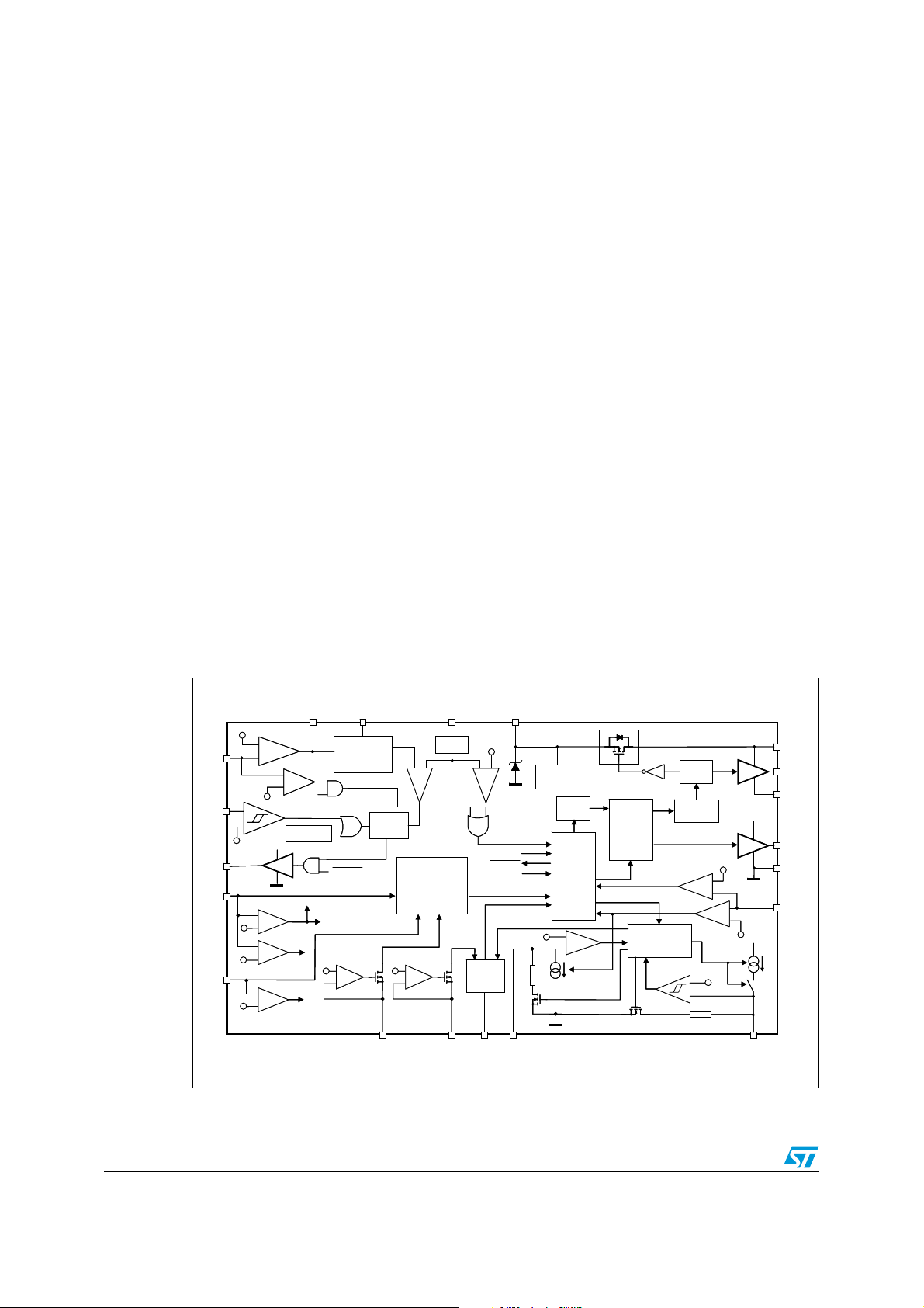
Figure 1. Block diagram
COMP MULT PFCS Vcc
COMP MULT PFCS Vcc
2.5V
2.5V
E/A
ZCD
ZCD
PFG
PFG
CTR
CTR
EOLR
EOLR
E/A
+
+
_
1.2V
1.2V
0.7V
0.7V
3.4V
3.4V
0.75V
0.75V
4.63V
4.63V
_
Vcc
Vcc
STARTER
STARTER
DIS
DIS
RELAMP
RELAMP
INV
INV
MULTIPLIER
MULTIPLIER
and THD
and THD
OPTIMIZER
OPTIMIZER
OL
OL
S
S
PFSTOP
PFSTOP
OL
OL
OVP
OVP
2V
2V
R
R
Q
Q
COMPARATOR
COMPARATOR
2V
2V
+
+
_
_
PWM
PWM
COMP.
COMP.
WINDOW
WINDOW
& REF.
& REF.
LEB
LEB
+
+
EOL
EOL
VCO
VCO
1.7V
1.7V
_
_
CHOKE
CHOKE
SAT.
SAT.
PFSTOP
PFSTOP
OVP
OVP
BOOT
Vcc
Vcc
0.9V
0.9V
Vcc
Vcc
BOOT
HSD
HSD
OUT
OUT
LSD
LSD
GND
GND
HBCS
HBCS
17V
17V
UV
UV
SYNCHRONOUS
DEAD
DEAD
TIME
TIME
CONTROL
CONTROL
LOGIC
LOGIC
SYNCHRONOUS
BOOTSTRAP DIODE
BOOTSTRAP DIODE
DRIVING
DRIVING
LOGIC
LOGIC
HB STOP
HB STOP
MANAGEMENT
MANAGEMENT
DETECTION
DETECTION
LATCH
LATCH
DIS
DIS
1.9V
1.9V
TIMING
TIMING
HVG
HVG
DRIVER
DRIVER
LEVEL
LEVEL
SHIFTER
SHIFTER
LVG DRIVER
LVG DRIVER
4.6
4.6
1.5
1.5
1.6V
1.6V
EOLP
EOLP
4/22
OSC EOIRF
OSC EOIRF
Tch
Tch
Page 5
AN2510 Device blocks description
2 Device blocks description
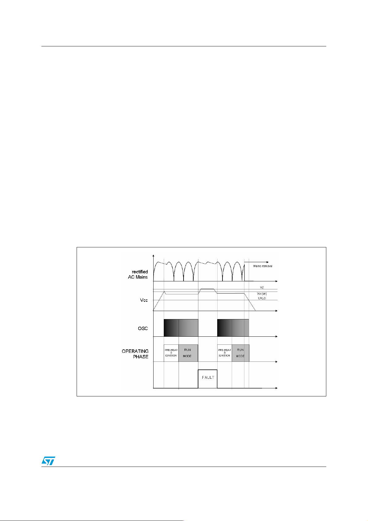
2.1 Start-up and shutdown
During start-up, the chip is supplied through a resistive path from the rectified AC Mains
voltage whereas during normal operation, a charge pump or a self-supply winding (as well
as an auxiliary converter) can provide the required current.
As the voltage at Vcc pin reaches the turn-on threshold (Vcc(ON)), the chip is enabled and
(unless a lamp absence is detected) the oscillator starts switching at a frequency set by
values of C
The Half-Bridge and the PFC sections start at almost the same time. As the
synchronization signal at pin ZCD is not yet generated by the external ZCD circuit, an
internal structure forces the PFC gate driver to switch for the first switching cycles. The
pulses are generated at a typical frequency of 15 kHz.
OSC
and R
RUN
and R
PRE
.
At shutdown, when the V
decreases below the UVLO threshold (either in case of Mains
CC
removal or in case of fault), the following conditions are met:
● all drivers are off;
● EOI pin is discharged (the internal switch is on);
● RF reference is disabled;
● Tch is discharged.
Figure 2. Start-up and shutdown sequences
5/22
Page 6
Device blocks description AN2510
2.2 PFC section
2.2.1 Error amplifier
The Error Amplifier (E/A) is used for frequency compensation. The inverting input (INV) is
connected by an external divider to the output bus and compares a partition of the boosted
output DC voltage, Vo, with the internal reference in order to maintain the pre-regulator
output DC voltage constant.
The compensation network, placed between pins INV and COMP (E/A output), is usually
done with a feedback capacitor. The E/A bandwidth will be extremely low because the
output of the E/A must be constant over a line half-cycle to achieve high PF.
The dynamics of the E/A output is internally clamped so that it can swing between 2.25 V
and 4.2 V in order to speed up the recovery after the E/A saturates low due to an overvoltage or saturates high because of an over-current.
Figure 3. Error amplifier, feedback divider and CTR
PFC OUTPUT
PFC OUTPUT
OVP
OVP
DISABLE
DISABLE
MULT
MULT
R1
R1
R2
R2
RHOVP
RHOVP
RLOVP
RLOVP
CTR
CTR
INV
INV
+
+
_
_
3.4V
3.4V
_
_
+
+
0.8V
0.8V
_
_
+
+
AMPLIFIER
NETWORK
NETWORK
AMPLIFIER
2.5V
2.5V
COMPENSATION
COMPENSATION
ERROR
ERROR
COMP
COMP
OPEN LOOP
OPEN LOOP
DETECTION
DETECTION
2.2.2 Over-voltage and feedback disconnection detection
The device is provided with a double over-voltage protection (OVP).
In case of over-voltage, the output of the E/A will tend to saturate low, but the E/A response
is very slow, so it will take a long time to go into saturation. On the other hand, an overvoltage must be corrected immediately.
A fast OVP detector, based on a different concept, is necessary.
The maximum voltage allowed for the PF output bus (VOVP) is defined by the resistive
divider connected to the pin CTR (Figure 3):
6/22
Page 7
AN2510 Device blocks description
Equation 1
R
HOVP
V
OVPVTH
⎛⎞
1
------------------+
•=
⎝⎠
R
LOVP
where V
is the CTR internal comparator input reference (3.4 V typ.)
TH
Moreover if the over-voltage lasts so long that the output of E/A goes below 2.25 V, the PF
gate driver is stopped until the E/A output goes back into its linear region.
If instead, the over-voltage is due to feedback disconnection (for example R1, Figure 3 fails
open), these two structures work together. In fact if the V
simultaneously the INV voltage falls below 1.2 V, typ. (due to the fact that the E/A source
capability is limited) the IC stops in a latched condition.
2.2.3 Zero Current Detection and triggering block
The Zero Current Detection (ZCD) block switches on the external PFC MOSFET as the
voltage across the boost inductor reverses, just after the current through the boost inductor
has gone to zero. This feature allows TM operation.
As the circuit is running, the signal for ZCD is obtained with an auxiliary winding on the
boost inductor. As at start-up no signal is coming from the ZCD, a circuit is needed that
turns on the external MOSFET. This is done with an internal starter, which forces the driver
to deliver a pulse to the gate of the MOSFET, producing also the signal for arming the ZCD
circuit.
The repetition rate of the starter is greater than ≅ 15 kHz and this maximum frequency must
be taken into account at design time.
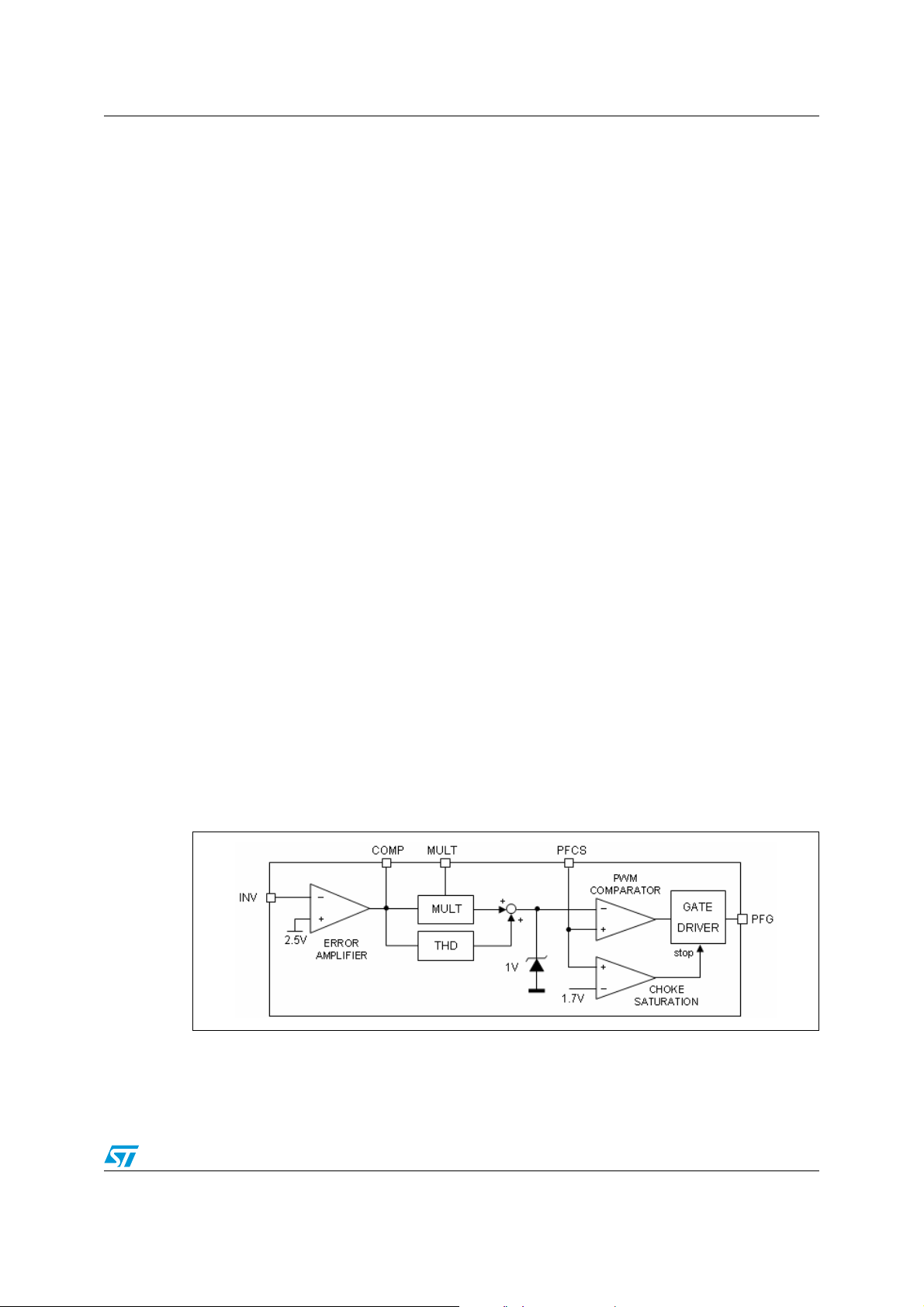
2.2.4 Multiplier block
threshold is crossed and
OVP
The multiplier (see Figure 4) has two inputs. The first one takes a partition of the
instantaneous rectified line voltage and the second one takes the output of the E/A. If this
voltage is constant (over a given line half-cycle), the output of the multiplier will be shaped
as a rectified sinusoid too. This is the reference signal for the current comparator, which sets
the MOSFET peak current cycle by cycle.
Figure 4. Multiplier, current sense and choke saturation
7/22
Page 8

Device blocks description AN2510
2.2.5 Current comparator and choke saturation detection
The current comparator (see Figure 4) senses the voltage across the current sense resistor
(Rs) and, by comparing it with the programming signal delivered by the multiplier,
determines the exact time that the external MOSFET is to be switched off.
The output of the multiplier is internally clamped to 1 V, (typ.). Current limiting occurs if the
voltage across Rs reaches this value.
A second comparator is integrated also in this block in order to prevent choke saturation
(see Figure 4 and Figure 5).
Boost inductor's hard saturation may be a fatal event for a PFC pre-regulator. The current
upslope becomes so large (50-100 times steeper, see Figure 5) that, during the current
sense propagation delay, the current may reach abnormally high values.
The device is provided with a second comparator on the PFC current sense pin that stops
and latches off the IC if the voltage on the pin, normally limited within 1.1 V, exceeds 1.7 V.
In this way there can be abnormal current only for one cycle. After that the system is
stopped and enabled to restart only after recycling the input power, that is when the Vcc
voltage of the L6585D goes below the UVLO threshold. System safety will be considerably
increased.
Figure 5. PFC choke saturation
2.2.6 Driver
A totem pole buffer, with 300mA source and 600 mA sink capability, allows driving an
external MOSFET. A pull-down circuit holds the output low when the device is in UVLO
conditions, to ensure that the external MOSFET cannot be turned on accidentally.
2.3 Oscillator and pre-heating / ignition / run mode sequencing
As the IC supply voltage (Vcc) reaches Vcc(on), the half-bridge starts oscillating and the
capacitor (C
current generator. When the voltage at T
generator switches off, and C
time constant R
During this time, the pin EOI is forced to ground and the switching frequency is set by the
oscillator capacitor together with the parallel of R
description in the following chapter.
8/22
) connected to TCH is charged with a constant current through the internal
D
discharges following an exponential decrease steered by the
, that defines the pre-heating time.
D*CD
D
pin reaches V
CH
RUN
and R
(4.63 V), the above current
CHP
(for the relationship, see pin
PRE
Page 9

AN2510 Device blocks description
When the voltage at pin TCH drops down to 1.53 V (typ.), the pin EOI is driven in high
impedance state and C
by C
IGN*RPRE
that defines the ignition time. At the same time the pin TCH is connected to
ground through an internal low resistance that rapidly discharges C
is exponentially charged according to the time constant τ given
IGN
.
D
The exponential trend of the current sunk by the pin RF generates a similar variation
(reduction) of the switching frequency. The voltage across the lamp increases linearly as
well as the current flowing through it.
As the voltage at EOI exceeds 1.9 V, the chip enters Run mode and remains in this condition
unless one of the protections (all enabled in this mode) is triggered.
Figure 6. Oscillator and starting sequence
2.4 Half-bridge current sensing: lamp voltage / power control
The information about the lamp current can be obtained by reading the voltage across the
sense resistor. This circuitry is enabled at the end of the pre-heating phase and it enriches
the L6585D with two features:
2.4.1 Controlled lamp voltage/current during ignition
If the V
This allows both limiting the ignition lamp voltage to a selectable (and safe) value and
preventing the risk of working below the resonance frequency of the L
(no saturation and no capacitive mode). The sense resistor value defines the maximum
current that can flow during ignition. With some calculations it is possible to find the relevant
lamp voltage (which must be higher than the nominal lamp voltage) and the corresponding
frequency, that is, the operating point on the resonance curve.
high threshold is crossed, then the chip reacts with a small frequency increase.
HBCS
BALLAST
- C
RES
circuit
9/22
Page 10

Device blocks description AN2510
Figure 7. Lamp voltage growth during ignition
Whenever the HBCS voltage reaches the internal threshold HBCSH, a two-step sequence
starts:
1. The internal current generator at the pin T
is turned on which charges CD (up to 4.6
CH
V) and starts a Tch charge/discharge cycle;
2. As long as the HBCS voltage exceeds the threshold, a controlled current pulse is sunk
by the EOI pin stopping the C
capacitor charge. This has the effect of stopping the
IGN
half-bridge switching frequency shift which limits the lamp voltage.
Tch acts as a counter. If the lamp ignites before TCH reaches 1.53 V (Figure 8 left), that is,
EOI has exceeded 1.9 V, then:
● EOI internal switch opens and its voltage moves asymptotically to 2 V
● The switching frequency reaches the operating frequency
● When TCH reaches 1.53, it will be discharged
If instead at the first low-side conduction cycle after the T
reaches 1.53 (EOI pin is still
CH
below 1.9 V), the HBCS threshold is still crossed, it means that the lamp hasn't ignited after
a time length equal to the pre-heat time (Figure 8 right). Such situations typically happen
with old lamps. In this case the oscillator stops, the chip enters low consumption mode, and
this condition is latched until the mains supply voltage is removed or a re-lamp is detected.
10/22
Page 11

AN2510 Device blocks description
Figure 8. Ignition as the lamp gets older
2.4.2 Over-current protection during run mode
If the HBCSL threshold is crossed, the TCH internal generator is turned on as well as the
one at pin EOI causing a frequency increase. This implements a CURRENT-CONTROL
structure (Figure 9 left). Simultaneously the internal T
C
up to 4.63 V and then released. If, despite the frequency increase, the over-current
D
generator is activated to charge the
CH
condition lasts for a whole Tch charge/discharge cycle, the IC is stopped and enters
shutdown mode by latching this condition until either a re-lamp or an UVLO (mains
removal). During run mode another protection is active: a second comparator (HBCSH) on
the pin HBCS detects anomalous current flow through the sense resistor such as the spikes
generated by the capacitive mode. The crossing of this second threshold latches the IC
(Figure 9 right).
Figure 9. Current control in run mode
11/22
Page 12

Device blocks description AN2510
2.5 End of life
2.5.1 End-of-life detection
This function has been designed to detect the aging of the lamp with particular attention to
the effect appearing as asymmetric rectification. The idea is to measure the variation of the
DC component of the lamp voltage that can be either positive or negative. A window
comparator has been introduced (centered around V
when the EOL-R voltage is higher than V
+ VW/2 or lower than V
SET
two standard ballast configurations (lamp-to-ground and block capacitor-to-ground) require
different features to the EOL detecting circuit, the implemented structure is compliant to both
thanks to the programmability of the window comparator. In particular through the resistor
connected to the EOLP pin, it is possible to select the sensing mode (with fixed reference or
reference to tracking with the PFC output bus) and the window amplitude (see the "pin
biasing" paragraph for further details).
● Lamp-to-ground (Figure 10, right): a resistive divider (R
across the lamp that, under normal conditions, is an AC signal with zero average value
whereas in case of asymmetric rectification, the DC value can shift either in a positive
or negative direction. As the L6585D doesn't have a negative rail, we must shift the
external signal. This can be done using two Zener diodes connected back-to-back
between the EOL pin and the center of the resistive divider. The Zener voltages should
differ by an amount as close as possible to the double of the internal reference to have
a symmetrical detection. It can easily obtained from the following equations:
–V
–V
where V
UP
= V
UP
DOWN
and V
+ W/2 + VZ1 + V
REF
= V
DOWN
- W/2 - VZ2 - VR1
REF
are the VK values (equal in absolute value) that trigger the window
R2
comparator. Figure 10 shows an example of asymmetric rectification with positive shifting.
with amplitude "VW") that triggers
REF
and RE2) senses the voltage
E1
- VW/2. Although the
REF
Figure 10. Window comparator for rectifying effect detection
R
R
R
P1
P1
P1
R
R
R
P2
P2
P2
EOLP
EOLP
EOLP
+ W/2
+ W/2
+ W/2
–W/2
–W/2
–W/2
FH
FH
FH
INTERNAL
INTERNAL
INTERNAL
FIXED REF.
FIXED REF.
FIXED REF.
INPUT
INPUT
INPUT
(100Hz or 120Hz)
(100Hz or 120Hz)
(100Hz or 120Hz)
BOOT
BOOT
BOOT
HSD
HSD
HSD
EOLR
EOLR
EOLR
OUT
OUT
OUT
LSD
LSD
LSD
CTR
CTR
CTR
WINDOW
WINDOW
WINDOW
COMPARATOR
COMPARATOR
COMPARATOR
AMPLITUDE
AMPLITUDE
AMPLITUDE
or R
or R
or R
R
R
R
FL
FL
FL
HVBUS
HVBUS
HVBUS
PFC
PFC
PFC
OUT
OUT
OUT
V
V
V
CB
CB
CB
CTR
CTR
CTR
V
V
V
REF
REF
REF
V
V
V
EOLR
EOLR
EOLR
V
V
V
REF
REF
REF
HV BUS
HV BUS
HV BUS
C
C
C
BOOT
BOOT
BOOT
CTR
CTR
CTR
FIXED REF.
FIXED REF.
FIXED REF.
WINDOW
WINDOW
WINDOW
COMPARATOR
COMPARATOR
COMPARATOR
AMPLITUDE
AMPLITUDE
V
V
V
LAMP
LAMP
LAMP
V
V
V
K
K
K
R
R
R
E1
E1
E1
R
R
R
E2
E2
E2
PFC
/2
PFC
/2
PFC
/2
OUT
OUT
OUT
AMPLITUDE
EOLP
EOLP
EOLP
C
C
C
BLOCK
BLOCK
BLOCK
R
R
R
V
V
V
LAMP
LAMP
LAMP
V
+ W/2 + V
V
+ W/2 + V
V
+ W/2 + V
REF
REF
REF
V
V
V
K
K
K
V
– W/2 – VZ1–V
V
– W/2 – VZ1–V
V
– W/2 – VZ1–V
REF
REF
REF
V
V
V
+ W/2
+ W/2
+ W/2
REF
REF
REF
V
V
V
REF
REF
REF
V
–W/2
V
–W/2
V
–W/2
REF
REF
REF
V
V
V
EOLR
EOLR
EOLR
INTERNAL
INTERNAL
INTERNAL
INPUT
INPUT
INPUT
or R
or R
or R
FL
FL
FL
BOOT
BOOT
BOOT
FH
FH
FH
Z1
Z1
Z1
EOLR
EOLR
EOLR
+ V
+ V
+ V
HSD
HSD
HSD
OUT
OUT
OUT
LSD
LSD
LSD
C
C
C
BOOT
BOOT
BOOT
V
V
V
V
V
V
Z2
Z2
Z2
Z1
Z1
Z1
R2
R2
R2
R2
R2
R2
HV BUS
HV BUS
HV BUS
R
R
R
E2
E2
E2
C
C
C
BLOCK
BLOCK
V
V
V
V
V
V
K
K
K
BLOCK
LAMP
LAMP
LAMP
R
R
R
E1
E1
E1
12/22
Page 13

AN2510 Device blocks description
● Block capacitor-to-ground (Figure 10 left): in this case the resistive divider is placed
across the block capacitor to sense its DC voltage. The asymmetric effect appears as
a shifting of this DC value that under normal conditions equals one half of the PFC
output voltage. A problem is that the ripple at twice the Mains frequency superimposed
on the PFC nominal voltage (the amplitude of this depends on the bulk capacitor value)
as well as any drop on the same voltage (Mains dips, missing cycle etc.) are present
also on the block capacitor voltage and they must be rejected by the end-of-life
detection circuit. For this reason a differential sense is necessary where the reference
for EOLR is not fixed but brings this information. In particular the reference for EOLR is
obtained by the CTR voltage value. The dividers R
and RE2 and RP1 and RP2 must
E1
be designed to make EOL-R voltage equal to CTR under nominal conditions. The
rejection of the PFC output voltage low frequency ripple allows using a smaller bulk
capacitance. The pin EOLP allows choosing:
– the EOL reading method: tracking reference or fixed reference;
– the EOL window amplitude (2 options).
To avoid an immediate intervention of the EOL protection, a filtering is introduced. As long
as the fault condition persists, the Tch internal generator charges the C
up to 4.63 V and
D
then it opens. If this fault condition is still present when the Tch voltage decreases down to
1.53, then the half bridge is stopped.
This fault condition drives the chip in an idle state characterized by low consumption.
Exiting from this condition is enough to cycle the re-lamp comparator. The discharge of the
Vcc voltage below the UVLO threshold leads to a reset of this condition.
2.6 Re-lamp comparator
A second comparator has been introduced on the pin EOL-R. A voltage higher than the
internal threshold is read as lamp absence so the chip suddenly stops switching, enters idle
mode (low consumption), and is ready for a new pre-heating/ignition sequence as soon as
a new lamp is inserted.
In this idle mode the consumption of the chip is reduced so that the current flowing through
the resistors (connected to the high voltage bus for the start-up) is enough to keep the Vcc
voltage above the UVLO threshold. After a re-lamp (that is, the EOL-R voltage is below the
re-lamp threshold), a new pre-heating/ignition sequence restarts.
Figure 11. Re-lamp comparator
OSC
EOL-R
Tch
13/22
Page 14

L6585 Biasing circuitry (pin by pin) AN2510
3 L6585 Biasing circuitry (pin by pin)
3.1 Pin1 OSC
Pin 1 is one of the two oscillator inputs. The value of the capacitor connected to ground
defines the half-bridge switching frequency in each operating state. Typically 330 pF/470 pF
capacitance values are used. The negative lead of the capacitor must be connected to a
signal ground, not affected by noise or spikes (for example, like those of the return path of
the half-bridge low side MOSFET) in order to maintain the oscillator accuracy.
3.2 Pin2 RF
Pin 2 is a 2 V reference able to source up to 240 µA (min.). The current sunk by this pin,
combined with the oscillator capacitance defines the half-bridge switching frequency in each
operating state.
A resistor connected to ground sets the run frequency while during pre-heating the
switching frequency is set by the parallel of the above resistance with the one connected
between pins RF and EOI (that is, a short circuit during pre-heating) according to the
following formula:
Equation 2
Equation 3
Where K is 1.328
The design flux is:
1. Choose Cosc
2. Set R
3. Set R
4. Set C
in order to obtain the desired run frequency;
RUN
in order to obtain the desired pre-heating frequency
PRE
in order to obtain the desired ignition time (see pin 3 description).
IGN
3.3 Pin3 EOI
Pin 3 is a multi-function pin. During pre-heating the pin is internally shorted to ground by the
logic so the resistor connected between and ground (R
frequency. During ignition it becomes high impedance. The ignition time is the time
necessary to the pin voltage to exponentially rise from zero to 1.9V. The growth is steered by
the R
PRE*CIGN
heating frequency, C
time constant. As the R
f
PRE
f
RUN
fixes the ignition time.
IGN
-----------------------------------------------------------------=
()C
R
PRERRUN
PRE
K
||
-----------------------------------------=
R
RUNCOSC
•
OSC
K
•()
) sets the pre-heating switching
PRE
value has already been chosen to set the pre-
14/22
Page 15

AN2510 L6585 Biasing circuitry (pin by pin)
3.4 Pin4 TCH
Pin 4 is the time counter and it is activated at pre-heating as well as after a protection
triggering (HBCS crossing during ignition / run mode, window comparator at EOL). To
achieve this, a RC parallel network is connected between this pin and ground. Firstly an
internal current generator (i
becomes high impedance and the R
both the pre-heating (T
of:
–T
–T
, charge time: pin voltage from 0 to 4.63 V →
CH
, discharge time: pin voltage from 4.63 V to 1.5 V →
DIS
So:
Equation 4
T
Sensible values for C
are from 220 nF to 1 µF; for example, choosing CD=680 nF, to obtain
D
a pre-heating of 1 s, we need:
) charges the above network up to 4.63 V after which the pin
ch
) and fault persistence (T
PRE
PRETCOUNT
discharge take place. The TCH cycle representing
DCD
C
D
-------- -
4.63 RD+• CDIn
I
CH
) time durations equals the sum
COUNT
C
D
CH
4.63
⎛⎞
-----------
••==
⎝⎠
-------- -
I
T
1.5
CH
4.63•=
DIS
RDCD• In
T
4.63
⎛⎞
-----------
•=
⎝⎠
1.5
Equation 5
3.5 Pin5 EOLP
Pin 5 is a 2 V reference and allows programming the window comparator of the pin 6
(EOLR) according to Ta bl e 1 :
Table 1. Window comparator settings
EOLP Reference Window amplitude
R
> 620 K Fixed 2.5 V ± 720 mV
EOLP
220 K = R
75 K = R
22 K = R
EOLP
EOLP
EOLP
3.6 Pin6 EOLR
C
D
PRE
CDIn
•
-------- -
I
CH
4.63
-----------
1.5
4.63•–
1.2M==
T
---------------------------------------------- -
R
D
= 270 K Tracking with CTR ± 220 mV
= 91 K Fixed 2.5 V ± 220 mV
= 27 K Tracking with CTR ± 720 mV
Pin 6 is the input of both the window comparator and a re-lamp comparator. Concerning the
window comparator, in case of tracking with CTR (suitable when the block capacitor is
referred to ground) the center is the same voltage as the pin CTR (V
). The resistive
CTR
divider connected across the block capacitor must be set such that, under normal
conditions:
15/22
Page 16

L6585 Biasing circuitry (pin by pin) AN2510
T
Equation 6
R
EL
---------------------------
V
EOLR
V
BLOCKDC
•=
RELRHL+
where V
BLOCKDC
output voltage. The 100/120 Hz ripple can be neglected because it is rejected by the
sensing structure.
3.7 Pin7 CTR
Pin 7 is a multifunction pin, connected to a resistive divider to the PFC output bus:
● PFC over-voltage
– In case of PFC output overshoot (for example at start-up) that causes a threshold
crossing, the PFC section stops switching until the voltage at the pin falls below
3.26 V. This is helpful because the bandwidth of the PFC error amplifier is narrow
so the control loop is not fast enough to properly react.
● Feedback disconnection
– The OVP function described above (together with the static one embedded in the
PFC error amplifier) is able to handle "normal" over-voltage conditions (those
resulting from an abrupt load/line change or occurring at start-up). In case of overvoltage generated when the upper resistor of the feedback output divider fails
open, the control loop can no longer read the information on the output voltage
and will force the PFC pre-regulator to work at maximum ON time. If this occurs
(that is, the pin INV falls below 1.2 V) and the CTR detects an OVP, the gate drive
activity is immediately stopped, the device is shut down, its quiescent
consumption is reduced below 250 µA, and the condition is latched as long as the
supply voltage of the IC is above the UVLO threshold;
● Reference for EOL in case of tracking reading.
is the DC value of the block capacitor voltage that is, one half of the PFC
Disable: by forcing the pin below 0.75 V an immediate unlatched shut-down is activated.
3.8 Pin8 MULT
Pin 8 is the second multiplier input. It will be connected, through a resistive divider, to the
rectified mains to get a sinusoidal voltage reference. The multiplier can be described by the
relationship: where V
V
CS
kV
COMP
2.5V–()• V
for the current sense, k is the multiplier gain, V
V
is the voltage on pin 8.
MULT
3.9 Pin9 COMP
Pin 9 is the output of the E/A and also one of the two inputs of the multiplier. A feedback
compensation network, placed between this pin and INV (10), reduces the bandwidth so to
avoid the attempt of the system to control the output voltage ripple (100-120 Hz). In the
simplest case, this compensation is just a capacitor, which provides a low frequency pole as
well as a high DC gain. A simple criterion to define the capacitance value is to provide ~60
dB attenuation at 100 Hz:
16/22
•=
MUL
COMP
(Multiplier output) is the reference
CS
is the voltage on pin 9 (E/A output) and
Page 17

AN2510 L6585 Biasing circuitry (pin by pin)
Equation 7
10
C
COMP
------------------------- -=
•
2 π• R
1
3.10 Pin10 INV
Pin 10 leads to both the inverting input of the E/A and to the open loop (feedback
disconnection) circuit. A resistive divider (Figure 3) will be connected between the regulated
output voltage of the boost and the pin. The internal reference on the non-inverting input of
the E/A is 2.5 V so R1 and R2 (Figure 3) will be then selected as follows:
Equation 8
R
2
V
PFOUT
⎛⎞
2.5 1
•=
⎝⎠
------ -+
R
1
3.11 Pin11 ZCD
Pin 11 is the input to the Zero Current Detector circuit. The ZCD pin will be connected to the
auxiliary winding of the boost inductor through a limiting resistor. The ZCD circuit is
negative-going edge-triggered. When the voltage on the pin falls below 0.7 V the PWM
latch is set and the MOSFET is turned on. To do so, however, the circuit must be armed first.
Prior to falling below 0.7 V the voltage on pin 11 must experience a positive-going edge
exceeding 1.4 V (due to MOSFET's turn-off). The maximum main-to-auxiliary winding turn
ratio, m, has to ensure that the voltage delivered to the pin during MOSFET's OFF-time is
sufficient to arm the ZCD circuit. Then:
3.12 Pin12 PFCS
Pin 12 is the inverting input of the current sense comparator. As the voltage across the
sense resistor (proportional to the instantaneous inductor current) crosses the threshold set
by the multiplier output, the power MOSFET is turned off. The MOSFET will stay in OFFstate until the PWM latch is set again by the ZCD signal. An internal circuit (LEB, leading
edge blanking) blanks the comparator for 200 ns in order to avoid undesired MOSFET turnoff due to the initial spike, present when the PFC is not operating in ZVS (that is when the
instantaneous voltage is higher than Vout/2).
The sense resistor value is calculated as follows:
V
CSpk
----------------
R
≤
S
–
The power dissipated in Rs, is given by:
–
I
Rspk
P
RSRSIQrms2
VO 2 V
--------------------------------------------------------
≤
m
•=
•–
irms max()
1.4
17/22
Page 18

L6585 Biasing circuitry (pin by pin) AN2510
The internal 1.16 V (max.) zener clamp on the non-inverting input of the PWM comparator
sets a current limitation threshold, so that the maximum current through Rs can be as high
as:
I
RSpkmax
This will be the maximum inductor current as well, therefore one must make sure that the
boost inductor does not saturate at this current level, which is very likely to be reached when
the boost converter is powered on (especially at low line) or powered off.
1.16
-----------=
R
s
3.13 Pin13 PFG
Pin 13 is the output of the driver. The pin is able to drive an external MOSFET with 300 mA
source and 600 mA sink capabilities.
3.14 Pin14 HBCS
Pin 14 is the half bridge current sense pin with 2-levels of current controls. The current
flowing in the HB MOSFET is sensed by a resistor. The resulting voltage is applied to this
pin. During the run mode both the low threshold (0.91 V) and the high threshold (1.6 V) are
active. In case of low thresholds crossing, the IC reacts with a self-adjusting frequency
increase in order to limit the half-bridge (lamp) current. In case of high threshold crossing
because of current spikes (due for example to capacitive mode / cross-conduction), the
L6585D latches to avoid damage to the MOSFET. During ignition only the high threshold
(1.6 V) is active. In case of crossing thresholds during the frequency shift, the IC reacts with
a self-adjusting frequency increase in order to limit the lamp voltage and prevent operation
below resonance.
3.15 Pin15 GND
This pin acts as the current return both for the signal internal circuitry and for the gate drive
current. When layouting the printed circuit board, these two paths should run separately.
3.16 Pin16 LSD
Pin 16 is the output of the half-bridge low side driver. The pin is able to drive an external
MOSFET with 290 mA source and 480 mA sink capabilities.
3.17 Pin17 V
Pin 17 is the supply of the device. This pin will be externally connected to the start-up circuit
(usually, one resistor connected to the rectified mains) and to the self-supply circuit.
Whatever the configuration of the self-supply system, a capacitor will be connected between
this pin and ground. To start the L6585D, the voltage must exceed the start-up threshold (15
V max.). Below this value the device does not work and consumes less than 350 µA from
Vcc. This allows the use of high value start-up resistors (in the hundreds kΩ), which reduces
18/22
CC
Page 19

AN2510 L6585 Biasing circuitry (pin by pin)
power consumption and optimizes system efficiency at low load, especially in wide range
mains applications.
When operating, the current consumption (of the device only, not considering the gate drive
current) rises to a value depending on the operating conditions but never exceeding 4.5 mA.
The device keeps on working as long as the supply voltage is over the UVLO threshold (11
V max). If the Vcc voltage exceeds 17.7 V max, an internal zener diode, 30 mA rated, will be
activated that clamps the voltage. In that case the power consumption of the device will
increase considerably, but there is no harm as long as the current is below the maximum
rating.
3.18 Pin18 OUT
Pin 18 is the High Side Driver Floating Reference. This pin must be connected close to the
source of the high side power MOS or IGBT.
3.19 Pin19 HSD
Pin 19 is the output of the half-bridge high side driver. The pin is able to drive an external
MOSFET with 290 mA source and 480 mA sink capabilities.
3.20 Pin20 BOOT
The supply of the high voltage section is obtained by means of a bootstrap circuitry. This
solution normally requires a high voltage fast recovery diode for charging the bootstrap
capacitor. In the L6585D a patented integrated structure replaces this external diode. It is
done by means of a high voltage DMOS, driven synchronously with the low side driver
(LVG), with a diode connected in series. To drive the synchronized DMOS it is necessary a
voltage higher than the supply voltage VS. This voltage is obtained by means of an internal
charge pump. The diode connected in series to the DMOS has been added to avoid
undesirable turn on it. The introduction of the diode prevents any current from flowing from
the BOOT pin to the VCC one if the supply is quickly turned off when the internal capacitor
of the pump is not fully discharged. The bootstrap driver introduces a voltage drop during
the recharging time of the capacitor C
with the frequency and with the size of the external power MOS. It is the sum of the drop
across the R
small and can be neglected. Increasing the frequency must be taken into account. In fact the
drop, reducing the amplitude of the driving signal, can significantly increase the R
the external power MOS (and so the dissipation). To be considered that in resonant power
supplies when we increase the frequency the current in mosfet's drain decreases. The
power dissipated by mosfet during the on-time is equal to Pcond=(Rds,on)*(Idrain)^2: then
Pcond is reduced when frequency is higher.
and of the diode threshold voltage. At low frequency this drop is very
DSON
(when the low side driver is on), which increases
boot
DSON
of
19/22
Page 20

L6585 Biasing circuitry (pin by pin) AN2510
Table 2. Fault conditions
Fault Condition IC behavior Action required
Lamp absence
than 4.63 V
(re-lamp
comparator)
Run mode: EOL-R voltage higher
than 4.63 V
At turn-on: EOL-R voltage higher
End of life
EOL-R voltage outside the limits of
window comparator
Ignition: HBCS threshold
Half-bridge
current sense
Run mode: HBCSL threshold
Run mode: HBCSH threshold
Shutdown CTR voltage lower than 0.8 V
– The T
charge does not start (no
CH
ignition)
– All drivers stopped
– IC low consumption (V
clamped)
cc
– All drivers stopped
– IC low consumption (V
(1)
–T
CH
cycle
(reset if the fault
clamped)
cc
disappears)
– All drivers stopped at the end of
cycle
T
CH
– IC low consumption (VCC
clamped)
–T
CH
cycle
with lamp voltage
(1)
control
– In case of HBCS at the end of the
cycle, all drivers stopped
T
CH
– IC low consumption (V
cycle
(1)
with lamp voltage
–T
CH
clamped)
cc
control (frequency increase)
– In case of HBCS at the end of the
TCH cycle, all drivers stopped
– IC low consumption (V
clamped)
cc
– All drivers stopped
– IC low consumption (V
clamped)
cc
– All drivers stopped
– IC low consumption (V
clamped)
cc
Lamp replacement
(EOL-R below 4.63 V)
Re-lamp cycle
Re-lamp cycle
Re-lamp cycle
Re-lamp cycle
(2)
(2)
(2)
(2)
When the CTR voltage
returns above 0.8 V,
the IC driver restarts
with a pre-heating
sequence
Choke
saturation
PFCS voltage higher than 1.6 V
– All drivers stopped
– IC low consumption (V
clamped)
cc
Re-lamp cycle
(2)
When the CTR voltage
Over-voltage of
PFC output
CTR voltage higher than 3.4 V
(typ.)
PFC driver stopped
returns below 3.26 V
(typ.), the PFC driver
restarts
PFC open loop
(feedback
disconnection)
1. T
cycle: charge of the TCH voltage up to 4.63 V and discharge down to 1.53 V following the RDCD time constant;
CH
2. Re-lamp cycle: the voltage at EOL-R pin must be first pulled above 4.63 V and then released below it; this typically happens
in case of lamp replacement. After a re-lamp cycle, a new pre-heating sequence will be repeated.
3. This fault actually is a "board" fault so a lamp replacement is not effective to restart the ballast
CTR voltage higher than 3.4 V
(typ.) and INV voltage lower than
1.2 V (typ.)
– All drivers stopped
– IC low consumption (V
clamped)
cc
Re-lamp cycle
(2)(3)
20/22
(3)
Page 21

AN2510 Revision history
4 Revision history
Table 3. Revision history
Date Revision Changes
26-Mar-2007 1 First issue
21/22
Page 22

AN2510
Please Read Carefully:
Information in this document is provided solely in connection with ST products. STMicroelectronics NV and its subsidiaries (“ST”) reserve the
right to make changes, corrections, modifications or improvements, to this document, and the products and services described herein at any
time, without notice.
All ST products are sold pursuant to ST’s terms and conditions of sale.
Purchasers are solely responsible for the choice, selection and use of the ST products and services described herein, and ST assumes no
liability whatsoever relating to the choice, selection or use of the ST products and services described herein.
No license, express or implied, by estoppel or otherwise, to any intellectual property rights is granted under this document. If any part of this
document refers to any third party products or services it shall not be deemed a license grant by ST for the use of such third party products
or services, or any intellectual property contained therein or considered as a warranty covering the use in any manner whatsoever of such
third party products or services or any intellectual property contained therein.
UNLESS OTHERWISE SET FORTH IN ST’S TERMS AND CONDITIONS OF SALE ST DISCLAIMS ANY EXPRESS OR IMPLIED
WARRANTY WITH RESPECT TO THE USE AND/OR SALE OF ST PRODUCTS INCLUDING WITHOUT LIMITATION IMPLIED
WARRANTIES OF MERCHANTABILITY, FITNESS FOR A PARTICULAR PURPOSE (AND THEIR EQUIVALENTS UNDER THE LAWS
OF ANY JURISDICTION), OR INFRINGEMENT OF ANY PATENT, COPYRIGHT OR OTHER INTELLECTUAL PROPERTY RIGHT.
UNLESS EXPRESSLY APPROVED IN WRITING BY AN AUTHORIZED ST REPRESENTATIVE, ST PRODUCTS ARE NOT
RECOMMENDED, AUTHORIZED OR WARRANTED FOR USE IN MILITARY, AIR CRAFT, SPACE, LIFE SAVING, OR LIFE SUSTAINING
APPLICATIONS, NOR IN PRODUCTS OR SYSTEMS WHERE FAILURE OR MALFUNCTION MAY RESULT IN PERSONAL INJURY,
DEATH, OR SEVERE PROPERTY OR ENVIRONMENTAL DAMAGE. ST PRODUCTS WHICH ARE NOT SPECIFIED AS "AUTOMOTIVE
GRADE" MAY ONLY BE USED IN AUTOMOTIVE APPLICATIONS AT USER’S OWN RISK.
Resale of ST products with provisions different from the statements and/or technical features set forth in this document shall immediately void
any warranty granted by ST for the ST product or service described herein and shall not create or extend in any manner whatsoever, any
liability of ST.
ST and the ST logo are trademarks or registered trademarks of ST in various countries.
Information in this document supersedes and replaces all information previously supplied.
The ST logo is a registered trademark of STMicroelectronics. All other names are the property of their respective owners.
© 2007 STMicroelectronics - All rights reserved
STMicroelectronics group of companies
Australia - Belgium - Brazil - Canada - China - Czech Republic - Finland - France - Germany - Hong Kong - India - Israel - Italy - Japan -
Malaysia - Malta - Morocco - Singapore - Spain - Sweden - Switzerland - United Kingdom - United States of America
www.st.com
22/22
 Loading...