

Page 1
AN2509
Application note
Wide range 400W (+200 V@1.6 A / +75 V@1 A)
L6599-based HB LLC resonant converter
Introduction
This note describes the performances of a 400W reference board, with wide-range mains
operation and power-factor-correction (PFC) and presents the results of its bench
evaluation. The electrical specification refers to a power supply for general purpose
application, with two main output voltages (200 V and 75 V).
The main features of this design are the very low no-load input consumption (<0.5 W) and
the very high global efficiency, better than 90% at full load and n ominal mains v o ltage (115 230 V
The circuit consists of three main bloc ks. The first is a front-end PFC pre-re gulator based on
the L6563 PFC controller. The second stage is a multi-resonant half-bridge converter with
two output volta ges of +200 V/300 W a nd 75 V/75 W, whose control is implemented through
the L6599 resonant controller. A further auxiliary flyback converter based on the VIPer12A
off-line primary switcher completes the architecture. This third block, deliv ering a total power
of 7 W on two output voltages (+3.3 V and +5 V), is mainly intended for microprocessor
supply and display power management operations
AC
).
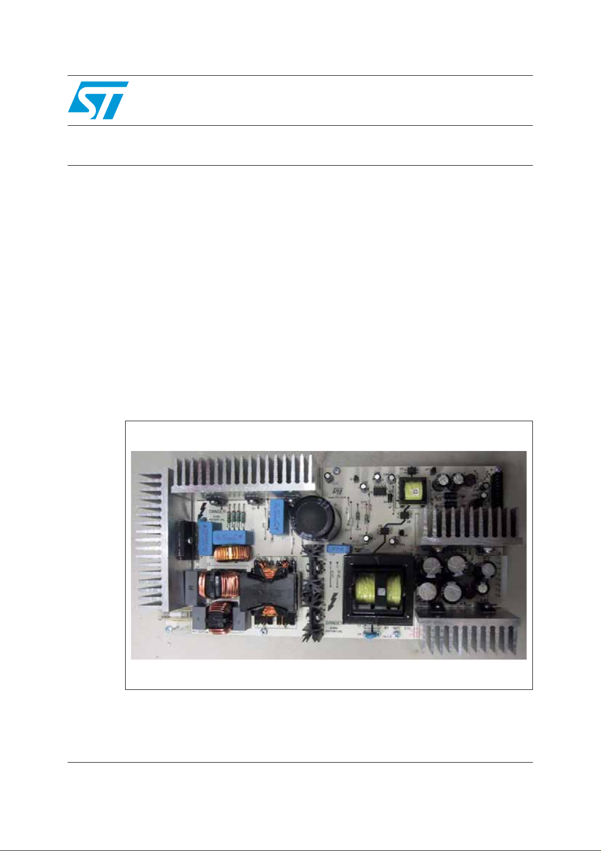
L6599 & L6563 400W demonstration board
April 2007 Rev 3 1/37
www.st.com
Page 2

Contents AN2509
Contents
1 Main characteristics and circuit description . . . . . . . . . . . . . . . . . . . . . 4
2 Electrical test results . . . . . . . . . . . . . . . . . . . . . . . . . . . . . . . . . . . . . . . . 9
2.1 Harmonic content measurement . . . . . . . . . . . . . . . . . . . . . . . . . . . . . . . . 9
2.2 Efficiency measurements . . . . . . . . . . . . . . . . . . . . . . . . . . . . . . . . . . . . . 10
2.3 Resonant stage operating waveforms . . . . . . . . . . . . . . . . . . . . . . . . . . . 12
2.4 Standby and no-load power consumption . . . . . . . . . . . . . . . . . . . . . . . . 17
2.5 Short-circuit protection . . . . . . . . . . . . . . . . . . . . . . . . . . . . . . . . . . . . . . . 17
2.6 Overvoltage protection . . . . . . . . . . . . . . . . . . . . . . . . . . . . . . . . . . . . . . . 19
3 Thermal tests . . . . . . . . . . . . . . . . . . . . . . . . . . . . . . . . . . . . . . . . . . . . . . 19
4 Conducted emission pre-compliance test . . . . . . . . . . . . . . . . . . . . . . 21
5 Bill of materials . . . . . . . . . . . . . . . . . . . . . . . . . . . . . . . . . . . . . . . . . . . . 23
6 PFC coil specification . . . . . . . . . . . . . . . . . . . . . . . . . . . . . . . . . . . . . . . 29
6.1 Electrical characteristics . . . . . . . . . . . . . . . . . . . . . . . . . . . . . . . . . . . . . . 29
6.2 Mechanical aspect and pin numbering . . . . . . . . . . . . . . . . . . . . . . . . . . . 29
7 Resonant power transformer specification . . . . . . . . . . . . . . . . . . . . . 30
7.1 Electrical characteristics . . . . . . . . . . . . . . . . . . . . . . . . . . . . . . . . . . . . . . 30
8 Auxiliary flyback power transformer . . . . . . . . . . . . . . . . . . . . . . . . . . . 32
8.1 Electrical characteristics . . . . . . . . . . . . . . . . . . . . . . . . . . . . . . . . . . . . . . 32
9 Board layout . . . . . . . . . . . . . . . . . . . . . . . . . . . . . . . . . . . . . . . . . . . . . . . 34
10 References . . . . . . . . . . . . . . . . . . . . . . . . . . . . . . . . . . . . . . . . . . . . . . . . 36
11 Revision history . . . . . . . . . . . . . . . . . . . . . . . . . . . . . . . . . . . . . . . . . . . 36
2/37
Page 3

AN2509 List of figures
List of figures
Figure 1. PFC pre-regulator electrical diagram . . . . . . . . . . . . . . . . . . . . . . . . . . . . . . . . . . . . . . . . . . 6
Figure 2. Resonant converter electrical diagram . . . . . . . . . . . . . . . . . . . . . . . . . . . . . . . . . . . . . . . . . 7
Figure 3. Auxiliary converter electrical diagram. . . . . . . . . . . . . . . . . . . . . . . . . . . . . . . . . . . . . . . . . . 8
Figure 4. Compliance to EN61000-3-2 standard for harmonic reduction: full load . . . . . . . . . . . . . . . 9
Figure 5. Compliance to EN61000-3-2 standard for harmonic reduction: 70 W load. . . . . . . . . . . . . . 9
Figure 6. Compliance to JEIDA-MITI standard for harmonic reduction: full load . . . . . . . . . . . . . . . . . 9
Figure 7. Compliance to JEIDA-MITI standard for harmonic reduction: 70 W load . . . . . . . . . . . . . . . 9
Figure 8. Power factor vs. Vin & load. . . . . . . . . . . . . . . . . . . . . . . . . . . . . . . . . . . . . . . . . . . . . . . . . 10
Figure 9. Total harmonic distortion vs. Vin & load . . . . . . . . . . . . . . . . . . . . . . . . . . . . . . . . . . . . . . . 10
Figure 10. Overall efficiency versus output power at nominal mains voltages. . . . . . . . . . . . . . . . . . . 12
Figure 11. Overall efficiency versus input mains voltage at various output power levels . . . . . . . . . . 12
Figure 12. Resonant circuit primary side waveforms at full load . . . . . . . . . . . . . . . . . . . . . . . . . . . . . 13
Figure 13. Resonant circuit primary side waveforms at light load (about 45 W output power) . . . . . . 14
Figure 14. Resonant circuit primary side waveforms at no load condition. . . . . . . . . . . . . . . . . . . . . . 14
Figure 15. Resonant circuit secondary side waveforms: +200 V output . . . . . . . . . . . . . . . . . . . . . . . 15
Figure 16. Resonant circuit secondary side waveforms: +75 V output . . . . . . . . . . . . . . . . . . . . . . . . 15
Figure 17. Low frequency (100 Hz) ripple voltage on +200 V and + 75 V outputs . . . . . . . . . . . . . . . 16
Figure 18. Load transition (0.16 A - 1.6 A) on +200 V output voltage . . . . . . . . . . . . . . . . . . . . . . . . . 16
Figure 19. +200 V output short-circuit waveforms . . . . . . . . . . . . . . . . . . . . . . . . . . . . . . . . . . . . . . . . 18
Figure 20. Thermal map @115 V
Figure 21. Thermal map at 230 V
Figure 22. Peak measurement on LINE at 115 V
Figure 23. Peak measurement on Neutral at 115 V
Figure 24. Peak measurement on LINE at 230 V
Figure 25. Peak measurement on Neutral at 230 V
Figure 26. Electrical diagram . . . . . . . . . . . . . . . . . . . . . . . . . . . . . . . . . . . . . . . . . . . . . . . . . . . . . . . . 29
Figure 27. Pin side view. . . . . . . . . . . . . . . . . . . . . . . . . . . . . . . . . . . . . . . . . . . . . . . . . . . . . . . . . . . . 30
Figure 28. Electrical diagram . . . . . . . . . . . . . . . . . . . . . . . . . . . . . . . . . . . . . . . . . . . . . . . . . . . . . . . . 31
Figure 29. Mechanical aspect and pin numbering . . . . . . . . . . . . . . . . . . . . . . . . . . . . . . . . . . . . . . . . 31
Figure 30. Winding position on coil former. . . . . . . . . . . . . . . . . . . . . . . . . . . . . . . . . . . . . . . . . . . . . . 32
Figure 31. Electrical diagram . . . . . . . . . . . . . . . . . . . . . . . . . . . . . . . . . . . . . . . . . . . . . . . . . . . . . . . . 33
Figure 32. Auxiliary transformer winding position on coil former . . . . . . . . . . . . . . . . . . . . . . . . . . . . . 33
Figure 33. Copper tracks . . . . . . . . . . . . . . . . . . . . . . . . . . . . . . . . . . . . . . . . . . . . . . . . . . . . . . . . . . . 34
Figure 34. Thru-hole component placing and top silk screen . . . . . . . . . . . . . . . . . . . . . . . . . . . . . . . 35
Figure 35. SMT component placing and bottom silk screen . . . . . . . . . . . . . . . . . . . . . . . . . . . . . . . . 35
- full load . . . . . . . . . . . . . . . . . . . . . . . . . . . . . . . . . . . . . . . . . . . 20
AC
- full load. . . . . . . . . . . . . . . . . . . . . . . . . . . . . . . . . . . . . . . . . . . 20
AC
and full load . . . . . . . . . . . . . . . . . . . . . . . . . . . . 21
AC
and full load. . . . . . . . . . . . . . . . . . . . . . . . . . . 21
AC
and full load . . . . . . . . . . . . . . . . . . . . . . . . . . . . 22
AC
and full load. . . . . . . . . . . . . . . . . . . . . . . . . . . 22
AC
3/37
Page 4

Main characteristics and circuit description AN2509
1 Main characteristics and circuit description
● The main characteristics of the SMPS are listed below:
● Universal input mains range: 90 to 264 V
● Output voltages: 200 V @ 1.5 A - 75 V @ 1 A - 3.3 V @ 0.7 A - 5 V @ 1 A
● Mains harmonics: compliance with EN61000-3-2 specifications
● Standby mains consumption: less than 0.5 W @230 V
●
Overall efficiency: better than 87% at full load, 90-264 V
●
EMI: Compliance with EN55022-class B specifications
● Safety: Compliance with EN60950 specifications
● PCB single layer: 132x265 mm, mixed PTH/SMT technologies
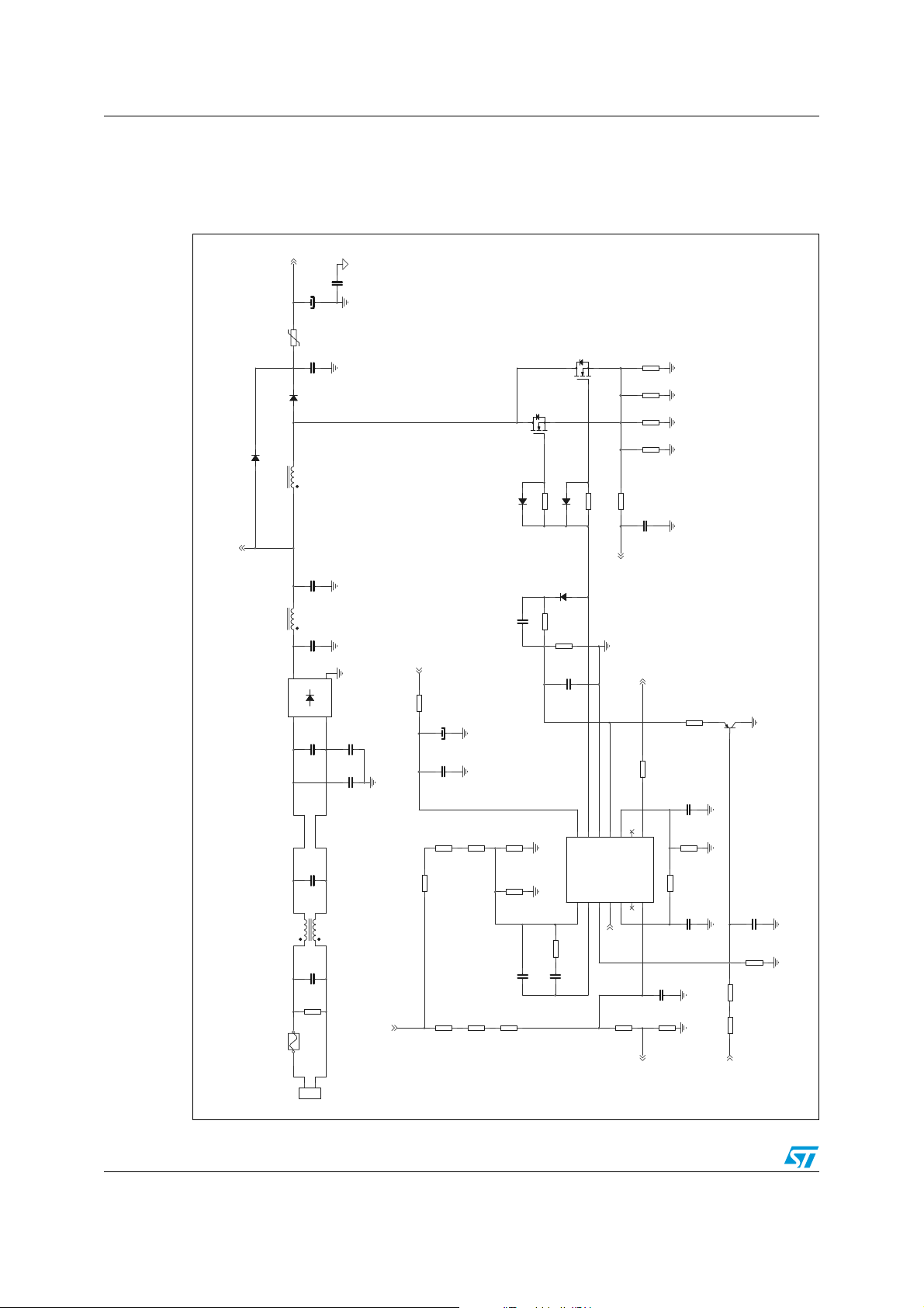
The circuit consists of three stages. A front-end PFC pre-regulator implemented by the
controller L6563 (Figure 1), a half-bridge resonant DC/DC conve rter based on the reson ant
controller L6599 (Figure 2), and a 7 W flyback converter intended for standby management
(Figure 3) utilizing the VIPer12A off-line primary switcher.
The PFC stage delivers a stable 400 VDC supply to the do wnstream con v erters (resonant +
flyback) and provides for the reduction of the current harmonics drawn from the mains, in
order to meet the requirements of the Euro pe a n no rm EN61000-3-2 and the JEIDA-MITI
norm for Japan.
- 45 to 65 Hz:
AC
AC
AC
The PFC controller is the L6563 (U1), integrating all functions needed to operate the PFC
and interface the downstream resonant converter. Although this controller chip is designed
for Transition-Mode (TM) operation, where the boost inductor wo rks next to the boundary
between Continuous (CCM) and Discontin uous Conduction Mode (DCM), by adding a
simple external circuit, it can be operated in LM-FOT (line-modulated fixed off-time). This
mode allows for CCM o perat ion, normally achie v ab le with more e x pensiv e contro l chips and
more complex architectures . The LM-F O T mode allows the use of a lo w-cost de vice lik e the
L6563 at a high power level, usually covered by CCM topologies. For a detailed and
complete description of the LM-FOT operating mode see the application note AN1792. The
external components to configure the circuit in LM-FOT mode are: C15, C17, D5, Q3, R14,
R17 and R29.
The power stage of the PFC is a conventional boost converter, connected to the output of
the rectifier bridge through a differential mode filtering cell (C5, C6 and L3) for EMI
reduction. It includes a coil (L4), a diode (D3) and two capacitors (C7 and C8). The boost
switch consists of two power MOSFETs (Q1 and Q2), connected in parallel, which are
directly driven by the L6563 output drive thanks to the high current capability of the IC.
The divider (R30, R31 and R32), connected to MULT pin 3, provides the information of the
instantaneous voltage that is used to modulate the boost current and to derive further
information like the average value of the AC line used by the V
(voltage feed-forward)
FF
function. This function is used to keep the output voltage almost independent of the mains.
The divider (R3, R6, R8, R10 and R11) is dedicated to detecting the output voltage while a
further divider (R5, R7, R9, R16 and R25) is used to protect the circuit in case of voltage
loop failure.
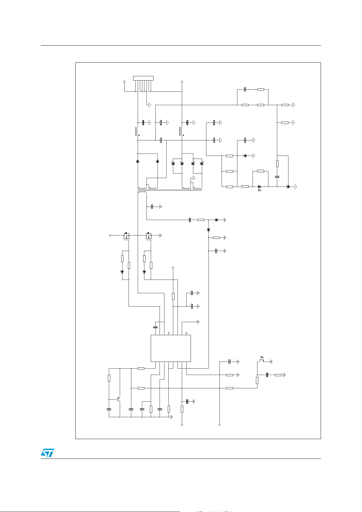
The second stage is an LLC resonant converter, with half-bridge topology implementation,
working in ZVS (zero voltage switching) mode.
4/37
Page 5

AN2509 Main characteristics and circuit description
The controller is the L6599 integrated circuit that incorporates the necessary functions to
properly drive the two half-bridge MOSFETs b y a 50 % fix ed duty cycle with fixed dead-time,
changing the frequency according to the feedback signal in order to regulate the output
voltages against load and input voltage variations. The main features of the L6599 are a
non-linear soft-start, a current protection mode used to program the hiccup mode timing, a
dedicated pin for sequencing or brown-out (LINE) and a standby pin (STBY) for burst mode
operation at light loads (not used in this design).
The transformer (T1) uses the magne tic integration approach, incorporating the resonant
series and shunt inductances of the LLC resonant tank. Thus, no additional external coils
are needed for the r esonance. F or a detaile d analysis of the LLC r esonant con v erter , please
refer to the application note AN2450.
The secondary side power circuit is configured with center- tap windings and two diodes
rectification for each outpu t (diod es D8A, D8B, D10A, D10B). The two center tap windings
are connected in series on the DC side (r efer to Figure 2). The +75 V rail is connected to
the center tap of the higher voltage winding (the one connected to the anodes of D8A and
D8B diodes). Therefore the higher v oltage windin g only has to provide a v oltage equal to the
difference of the two output voltages: 200 V - 75 V = 125 V. This winding arrangement has
the advantage of a better cross regulation with respect to the case of two completely
separated outputs. F urthermore, due to the fact that the +200 V diodes only have to
withstand a voltage of about 25 0 V (2 x 125 V), inst ead of about 400 V in case of complet ely
separated windings, the designer can select a diode with a lower junction capacitance
minimizing the effect of this capacitance refle ct ed at transformer primary side. This may
affect the behavior of the resonant tank, changing the circuit from LLC to LLCC type, with
the risk that the conv erter, in light-load/n o-load condition ( when the f e edbac k loop increa ses
the operating frequency), can no longer control the output voltage.
The feedbac k loop is implemented b y means of a classical con figuration using a TL431 (U4)
to adjust the current in the optocoupler diode (U3). The optocoupler transistor modu lates the
current from controller Pin 4, so the frequency will change accordingly, thus achieving the
output voltage regulation. Resistors R46 and R54 set the maximum operat ing frequency.
In case of a short circuit, the current entering the primary winding is detected by the lossless
circuit (C34, C39, D11, D12, R43, and R45) and the resulting signal is fed into L6599 Pin 6.
In case of overload, the voltage on Pin 6 exceeds an internal threshold that triggers a
protection sequence via Pin 2, keeping the current flowing in the circuit at a safe level.
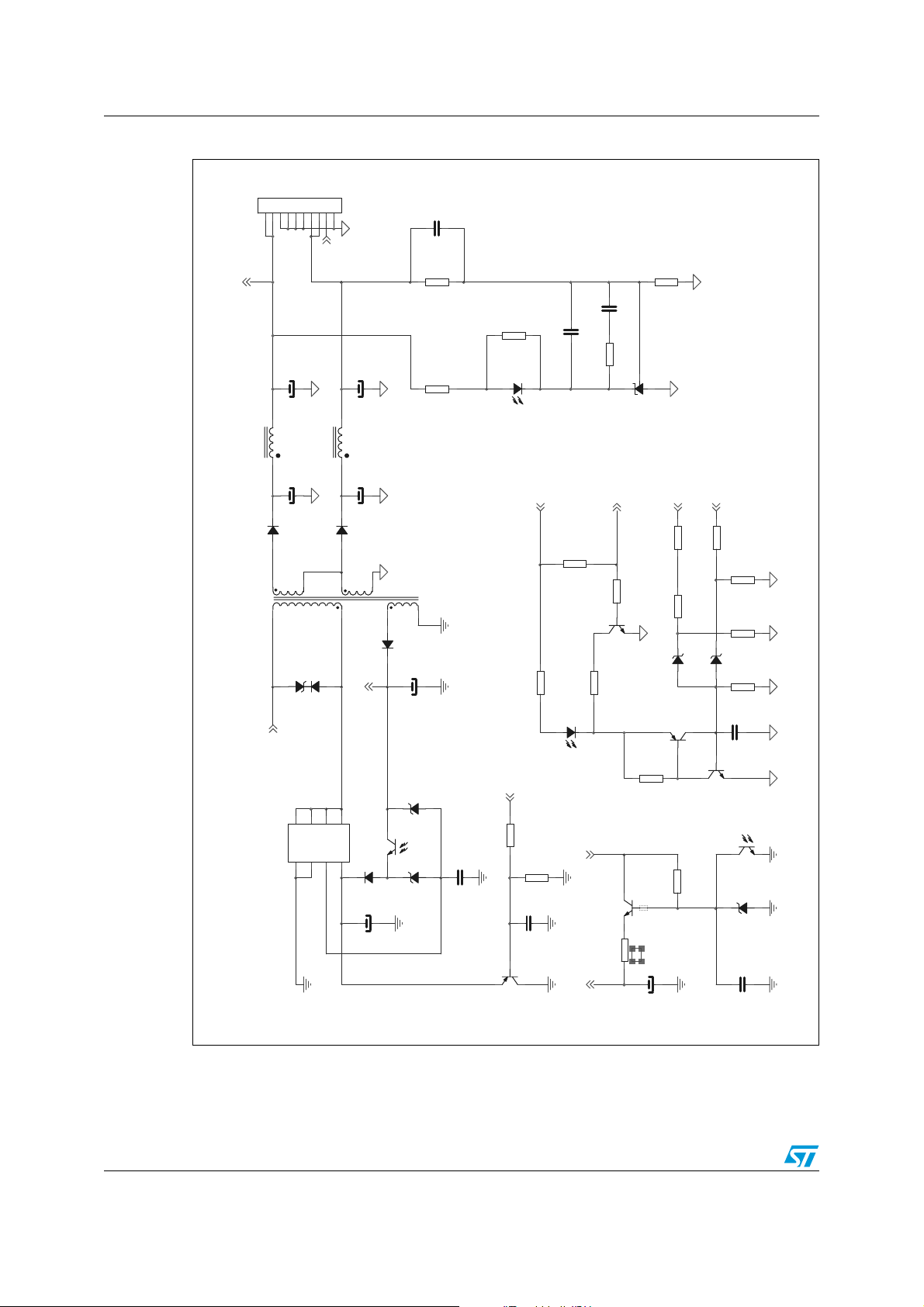
The third stage is a small flyback converter based on the VIPer12A, a current mode
controller with integrated power MOSFET, capable of delivering about 7 W total output
power on the output voltages (5 V and 3.3 V). The regulated output voltage is the 3.3V
output and, also in this case, the feedback loop uses the TL431 (U7) and optocoupler (U6)
to control the output volta ge.
This converter is able to operate in the whole mains voltage range, even when the PFC
stage is not working. From the auxiliary winding on the primary side of the flyback
transformer (T2), a voltage Vs is available, intended to supply the other controllers (L6563
and L6599) in addition to the VIPer12A itself.
The PFC stage and the resonant converter can be switched on and off through the circuit
based mainly on components Q7, Q8, D22 and U8, which, depending on the level of the
signal ST-BY, supplies or removes the auxiliary voltage (VAUX) necessary to start-up the
controllers of the PFC and resonant stages. When the AC input voltage is applied to the
power supply, the small flyback converter switches on first. Then, when the ST-BY signal is
asserted low, the PFC p re-regulator becomes oper ative , and last the resonant conv erter can
deliver the output power to the load. Note that if Pin 9 of Connector J3 is left floati ng (no
5/37
Page 6
Main characteristics and circuit description AN2509
signal ST-BY present), the PFC and resonant converter will not operate, and only +5 V and
+3.3 V supplies are availa ble on the output. In order to enable the +200 V and +75 V
outputs, Pin 9 of Connector J3 must be pulled down to ground.
Figure 1. PFC pre-regulator electrical diagram
Vdc
+400V
C9
2nF2-Y 1
330uF/450V
C8
R2
NTC 2R5-S237
C7
470nF/630V
D3
STTH8R06
1-2
D1
1N5406
L4
PQ40-500uH
5-6
D4
LL4148
Q2
STP12NM50FP
Q1
STP12NM50FP
D6
LL4148
R18
R15
6R8
6R8
R24
0R39
R23
0R39
R22
0R39
R21
0R39
R19
1k0
C18
330pF
Vrect
C6
470nF/630V
L3
DM-51uH-6A
C5
470nF/630V
Vaux
+
-
D2
D15XB60
~
~
C11
2
680nF-X2
Jumper
330nF-X2
470nF-X2
1M5
2nF2-Y2
C10
2nF2-Y2
CON2-IN
C4
Jumper
C3
L1
CM-1.5mH-5A
C2
R1
F1
8A/250V
1
J1
R4
47
C13
10uF/50V
C12
100nF
R6
680kR8680k
R3
680k
R5
Vdc
2M2
R11
R10
R7
2M2
R9
D5
C15
100pF
R14
3k3
R17
C17
15k
U1
L6563
100k
R13
56k
C14
100nF
C16
1uF
2M2
CSCS
LL4148
15k
220pF
GD
VCC
INV
COMP
ZCD
GND
MULTCSVFF
PWM-Latch
R29
1k5
Q3
BC857C
R20
1k0
C21
2nF2
R28
RUN
PWM-STOP
TBO
PFC-OK PWM-LATCH
R16
5k1
LINE
240k
R26
150k
C20
470nF
C19
10nF
R25
30k
C22
10nF
R32
10k
R31
620k
R30
620k
Vrect
6/37
Page 7
AN2509 Main characteristics and circuit description
Figure 2. Resonant converter electrical diagram
1234567
J2
+200V
L5
T1
8
CON8
C25
22uF/250V
C29
10uH
C30
D8A
T-RE S-ER 49- 400 W
D8B
BYT08P-400
BYT08P-400
C28
47nF/630V
+75V
C38
C35
100uF/250V
JP
100uF/250V
47uF/100V
L6
22uH
D10B
D10A
STTH1002C
STTH1002C
220uF/100V
C37
220uF/100V
R50
56k
R49
56k
R48
56k
R86
C59
R53
C41
D13
R52
470R
47nF
R61
75k
R58
75k
10uF/50V
C-12V
R56
1k0
3k3
U3A
SFH617A-2
2k7
R60
6k2
R59
1k0
C44
47nF
U4
TL431
R43
150
C34
220pF/630V
Vdc
Q5
R33
D7
R88
560k
Q12
BC557
C61
470nF
Q6
STP14NK50Z
0R
R35
47
LL4148
C23
100nF
STP14NK50Z
R39
0R
R40
47
D9
LL4148
C27 100nF
U2
L6599
R36
0R
R34
2k7
C24
470nF
R37
2M2
VBOOT
CSS
C26
OUT
HVG
DELAYCFRFMIN
270pF
R41
Vaux
C32
100nF
R38
47
C31
10uF/50V
NC
LVG
VCC
STBY
ISEN
LINE GND
DIS PFC-STOP
C33
4nF7
R42
10
16k
D11
LL4148
D12
LL4148
R45
100R
C39
1uF0
U3B
C40
10nF
R47
10k
R46
1k5
SFH617A-2
R87
220R
C60
470nF
R54
1k5
LINE
PWM-Latch
7/37
Page 8
Main characteristics and circuit description AN2509
Q10
BC847C
C54
100nF
U7
TL431
C53
2nF2
U6A
SFH617A-2
U6B
SFH617A-2
Vs
+200V
R67
1k0
SSFB
Vdd D
D
D
D
U5
VIPER-12A
R82
100k
R79
2k2
D15
1N5822
D16
1N5821
D20
BAV103
C56
100nF
C45
1000uF/10V
C47
1000uF/10V
C50
10uF/50V
C46
100uF/10V
C49
100uF/10V
Q9
BC857C
C48
10uF/50V
R76
150k
U8A
SFH617A-2
R75
150k
U8B
SFH617A-2
R74
10k
R77
4k7
D19
C-30V
St-By
D18
B-10V
123456789
10
J3
CON10
R69
0R
Vdc
C52
47nF
R68
22k
C51
100nF
R71
10k
Q8
BC847C
R72
10k
C55
10uF/50V
R66
1k0
T2
T-FLY -AUX-E20
+400V
R70
22R
Vdc
+400V
R83
1M0
R84
150k
C58
10nF
Q11
BC557C
+5Vst -by
R81
30k
R80
30k
+3V3
+5Vst-by
Q7
BC547C
D22
C-15V
L7
33uH
L8
33uH
D17
LL4148
+75V
D21
B-15V
D23
B-15V
R62
47
R64
1k6
C57
1nF0
Vs
Vaux
+5Vst -by
D14
PKC-136
St-By
R73
8k2
Figure 3. Auxiliary converter electrical diagram
8/37
Page 9
AN2509 Electrical test results
2 Electrical test results
2.1 Harmonic content measurement
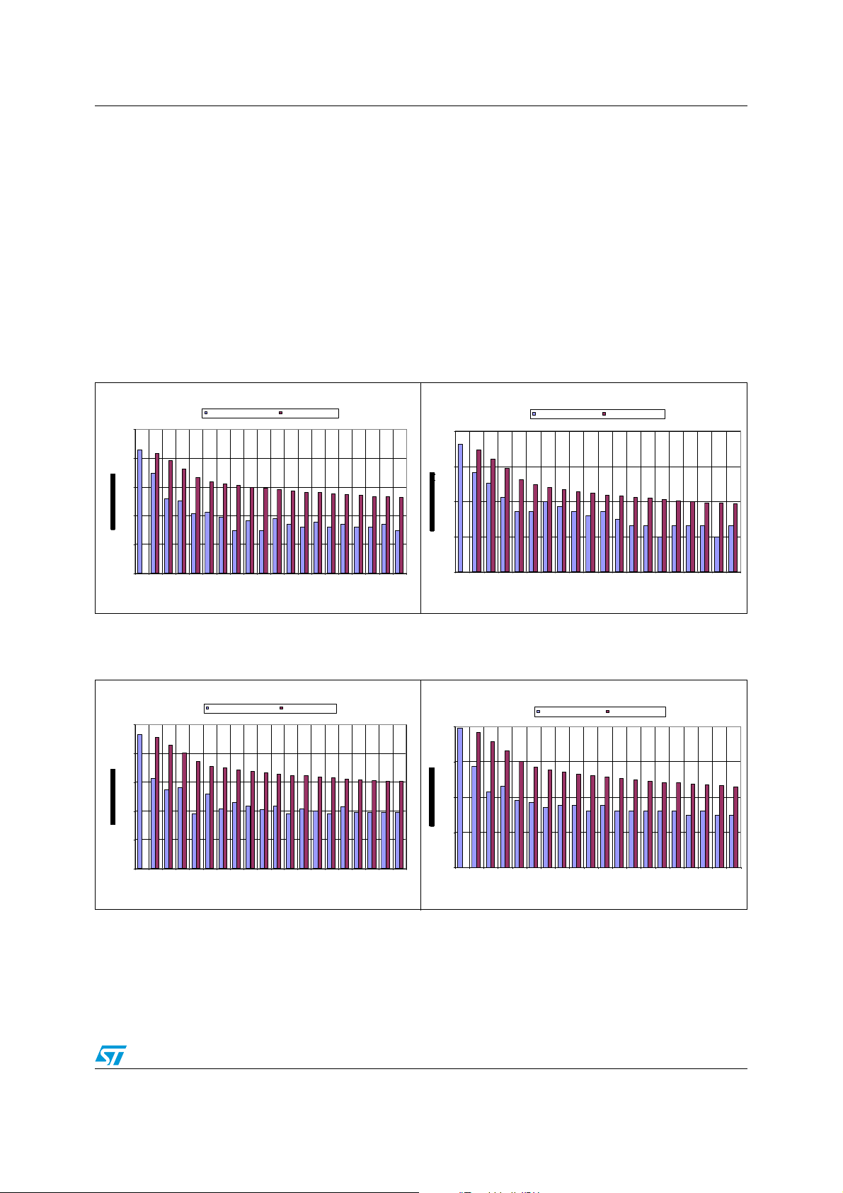
The current harmonics drawn from the mains have been measured according to the
European rule EN61000-3-2 Class-D and Japanese rule JEIDA-MITI Class-D, at full load
and 70 W output power, at both nominal input voltages (230 V
in Figure 4 to Figure 7 show that the measured current harmonics are well below the limits
imposed by the regulations , both at full-load and at 70 W load.
and 100 VAC). The graphs
AC
Figure 4. Compliance to EN61000 -3 -2
standard for harmonic reductio n :
10
1
0.1
0.01
0.001
0.0001
full load
Measurements @ 230Vac Full load EN61000-3-2 class D limit s
1234567891011121314151617181920
Harmoni c Order (n)
Figure 6. Compliance to JEIDA-MITI standard
10
for harmonic reduction: full load
Measurements @ 100Vac Full load J EIDA- M ITI c la ss D l im it s
Figure 5. Compliance to EN61000-3-2
standard for harmonic reduction:
70 W load
Measurement s @ 230Vac 70W EN61 000-3-2 cl ass D limits
1
0.1
0.01
0.001
0.0001
1 2 3 4 5 6 7 8 9 10 11 12 13 14 15 16 17 18 19 20
Harmoni c Order (n)
Figure 7. Compliance to JEIDA-MITI standard
for harmonic reduction: 70 W load
Measurement s @ 100V ac 70W JEI DA -MIT I cla s s D limits
1
1
0.1
0.01
0.001
0.0001
1234567891011121314151617181920
Harmoni c Order (n)
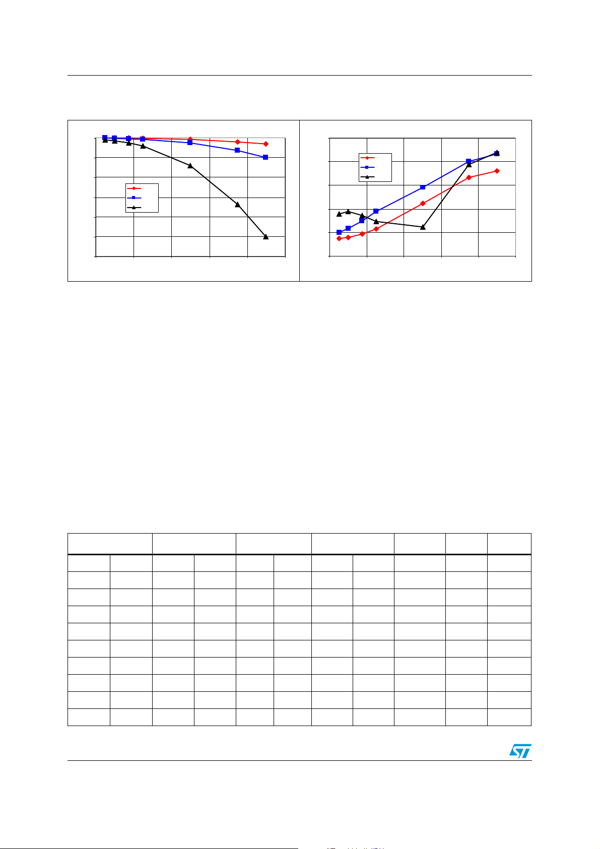
The Power Factor (PF) and the Total Harmonic Distortion (THD) are reported in Figure 8
and Figure 9. It is evident from the graph that th e PF stays close to unity in the whole mains
voltage range at full load and at half load, while it decreases at high mains at low load
(70 W). The THD has similar behavior, remaining within 25% overall the mains voltage
range and increasing at low load (70 W) at high mains voltage.
0.1
0.01
0.001
0.0001
1234567891011121314151617181920
Harmoni c Orde r (n )
9/37
Page 10
Electrical test results AN2509
Figure 8. Power factor vs. Vin & load Figure 9. Total harmonic distortion vs. Vin &
PF
1.00
0.98
0.95
0.93
0.90
0.88
0.85
80 120 160 200 240 280
400W
200W
70W
Vin [Vrms]
THD [%]
25.00
20.00
15.00
10.00
5.00
0.00
80 120 160 200 240 280
load
400W
200W
70W
Vin [Vrms]
2.2 Efficiency measurements
Table 1 and Table 2 show the output voltage measurements at the nominal mains voltages
of 115 V
load and at light load operations, the input power is measured using a Yokogawa WT-210
digital power meter. Particular attention has to be paid when measuring input power at full
load in order to avoid measurement errors due to the voltage drop on cables and
connections.
and 230 VAC, with different load condi tions. For all measurements, both at full
AC
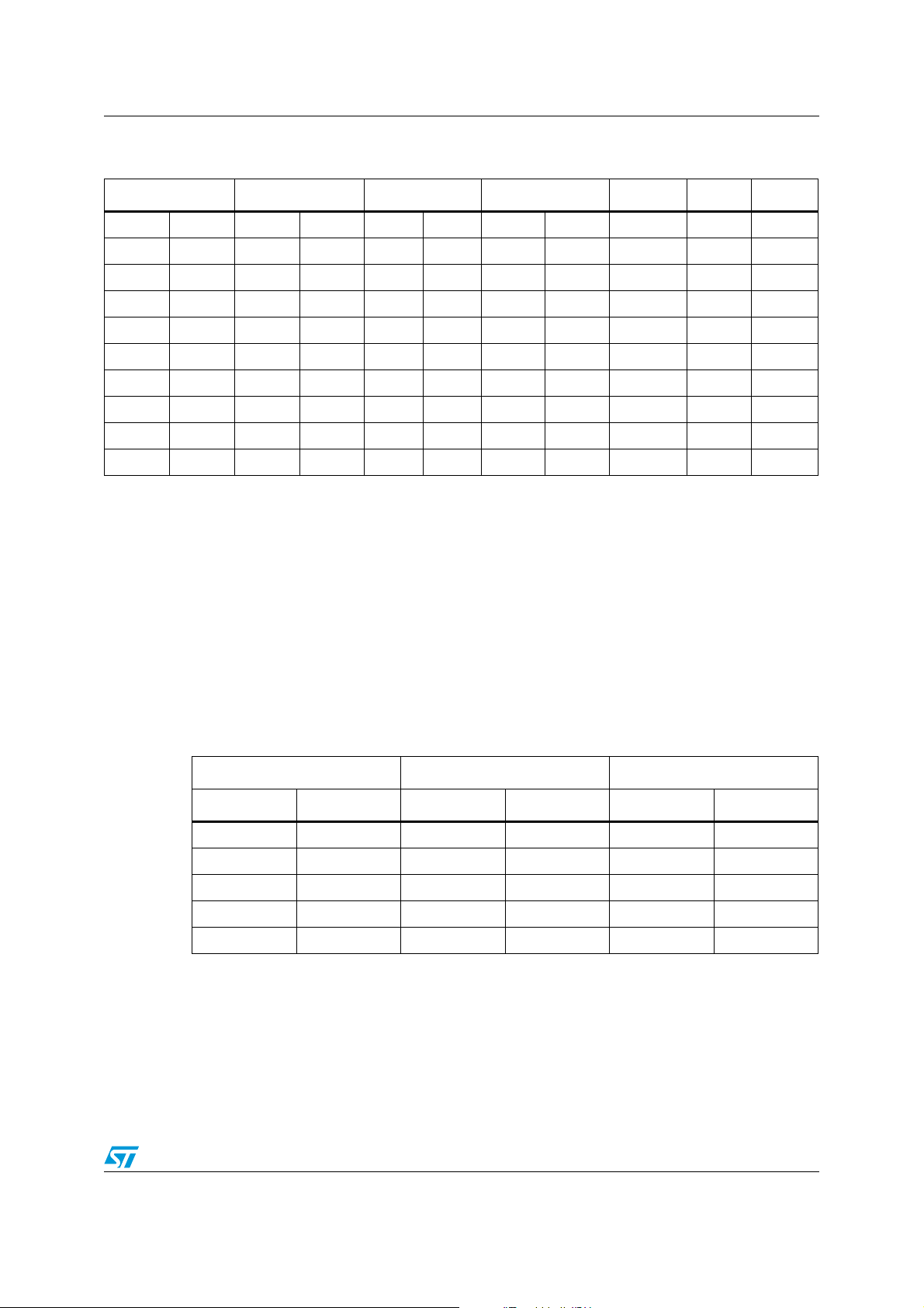
Figure 10 shows the overall circuit efficiency, measured at each load condition, at both
nominal input mains voltages of 115 V
and 230 VAC. The values were measured af ter 30
AC
minutes of warm-up at maximum load. The high efficiency of the PFC pre-regulator working
in FOT mode and the very high efficiency of the resonant stage working in ZVS (i.e. with
negligible switching losses), provides for an overall efficiency better than 87% at full load in
the complete mains voltag e r a ng e. This is a significant high value for a two-stage converter ,
especially at low input mains voltage where the PFC conduction losses increase. Even at
lower loads, the efficiency still remains high.
Table 1. Efficiency measurements @VIN = 115 V
+200 V @load(A) +75 V@load(A) +5 V @load(A) +3.3 V@load(A) POUT(W) PIN(W) Eff. %
200.29 1.591 77.77 1.020 4.88 0.975 3.33 0.695 405.06 433.30 93.48%
200.29 1.441 77.78 0.894 4.88 0.975 3.33 0.695 365.23 390.68 93.48%
200.31 1.281 77.78 0.801 4.88 0.975 3.33 0.695 325.97 348.98 93.41%
200.31 1.120 77.79 0.694 4.88 0.975 3.33 0.695 285.41 306.05 93.25%
200.32 0.962 77.79 0.600 4.88 0.502 3.33 0.352 243.00 260.90 93.14%
200.34 0.802 77.80 0.506 4.88 0.502 3.33 0.352 203.66 219.52 92.78%
200.34 0.642 77.80 0.399 4.88 0.502 3.33 0.352 163.28 177.37 92.06%
200.34 0.481 77.81 0.306 4.88 0.502 3.33 0.352 123.80 136.39 90.77%
200.40 0.321 77.83 0.199 4.86 0.144 3.33 0.097 80.84 91.34 88.50%
AC
200.43 0.161 77.83 0.105 4.86 0.146 3.33 0.099 41.48 50.48 82.17%
10/37
Page 11
AN2509 Electrical test results
Table 2. Efficiency measurements @V
+200 V @load(A) +75 V @load(A) +5 V @load(A) +3.3 V @load(A) POUT(W) PIN(W) Eff. %
200.32 1.593 77.78 1.022 4.88 0.977 3.33 0.695 405.68 449.65 90.22%
200.32 1.442 77.79 0.896 4.88 0.977 3.33 0.695 365.64 404.46 90.40%
200.32 1.282 77.80 0.802 4.88 0.977 3.33 0.695 326.29 360.10 90.61%
200.32 1.120 77.80 0.694 4.88 0.977 3.33 0.695 285.43 314.90 90.64%
200.35 0.962 77.80 0.600 4.88 0.502 3.33 0.351 243.04 267.18 90.96%
200.32 0.802 77.79 0.508 4.88 0.502 3.33 0.351 203.79 224.33 90.84%
200.31 0.641 77.79 0.399 4.88 0.503 3.33 0.351 163.06 180.53 90.32%
200.34 0.480 77.80 0.305 4.88 0.503 3.33 0.351 123.52 138.06 89.47%
200.40 0.321 77.83 0.197 4.86 0.144 3.33 0.097 80.68 91.83 87.86%
200.43 0.160 77.84 0.050 4.86 0.146 3.33 0.099 405.68 49.72 74.42%
= 230 V
IN
AC
The global efficiency at full load has been measured even at the limits of the input voltage
range, with good results:
At VIN = 90 V
At VIN = 264 V
- full load, the efficiency is 87.27%
AC
- full load, the efficiency is 93.49%
AC
Also at light load, at an output power of about 10% of the maximum level, the overall
efficiency is very good, reaching a v alue of about 75% a t nominal main s v oltag es. Figure 11
shows the efficiency measured at various output power levels versus input mains voltage.
The cross regulation of the resonant converter stage is very good as shown in Table 3,
where the +200 V and +75 V output v o ltages are measur ed in different load conditions, with
minimum output current equa l to 10% of maximum current for both the output volta ges.
Table 3. Cross regulation
230 V
AC
200 V load 75 V load 200 V 75 V 200 V 75 V
max max 200.26 77.77 200.32 77.78
max min 200.35 77.92 200.35 77.94
min max 200.35 77.58 200.35 77.58
min min 200.42 77.82 200.45 77.84
no-load no-load 200.76 77.66 200.76 77.65
115 V
AC
11/37
Page 12
Electrical test results AN2509
Figure 10. Overall efficiency versus output power at nominal mains voltages
230Vac 115Vac
95%
90%
85%
Eff. (%)
80%
75%
70%
0 50 100 150 200 250 300 350 400 450
Output Power (W)
Figure 11. Overall efficiency versus input mains voltage at various output power
levels
400W 200W 70W
Eff[%]
94%
93%
92%
91%
90%
89%
88%
87%
86%
85%
80 120 160 200 240 280
Vin [Vrms]
2.3 Resonant stage operating waveforms
Figure 12 shows some waveforms during steady state operation of the resonant circuit at full
load. The Ch1 waveform is the half-bridge square voltage on Pin 14 of L6599, driving the
resonant circuit. In the picture it is not e vident, but the switching frequency is normally
slightly modulated following the PFC pre-regulator 100-Hz ripple that is rejected by the
12/37
Page 13

AN2509 Electrical test results
resonant control circuitry. The Ch2 waveform represents the transformer primary current
flowing into the resonant tank. As shown, it has almost a sinusoidal shape. The resonant
tank has been designed (follo wing the pr ocedure present ed in the applica tion note AN2450)
to operate at a resonance frequency of about 120 kHz when the dc input voltage of the halfbridge circuit is at 390 V (that is the nominal output voltage of the PFC stage).
The resonant frequency has been selected at appr oximately 120 kHz in order to have a
good trade-off between transformer losses and dimens ion s.
The resonant tank circuit has been designed in orde r to have a good margin for ZVS
operation, providing good efficiency, while the almost sinusoidal current wavef orm allows for
an extremely low EMI generation.
Figure 12. Resonant circuit primary side waveforms at full load
Ch1: half-bridge square
voltage on pin 14 of L6599
Ch2: resonant tank current
Ch3: low side MOSFET
drive signal
Figure 13 and Figure 14 show the same waveforms as in Figure 12, when the resonant
converter is light-loaded (about 45 W) or not loaded at all. These two graphs demonstrate
the ability of the converter to operate down to zero load, with the output voltages still within
the regulation range.
The resonant tank current has ob viou sly a triangul ar shape and r epresen ts the m agnet izing
current flowing into the transformer primary side. The oscillation superimposed on the tank
current depends on the occurrence of a further resonance due to the parallel of the
inductances at primary side (the series and shunt inductances in the APR (all primary
referred) transformer model presented in AN2450) and the undesired se condary side
capacitance reflected at transformer primary side.
13/37
Page 14

Electrical test results AN2509
Figure 13. Resonant circuit primary side waveforms at light load (about 45 W outpu t
power)
Ch1: half-bridge square
voltage on pin 14 of L6599
Ch2: resonant tank current
Ch3: low side MOSFET
drive signal
Figure 14. Resonant circuit primary side waveforms at no load condition
Ch1: half-bridge square
voltage on pin 14 of L6599
Ch2: resonant tank current
Ch3: low side MOSFET
drive signal
In Figure 15 and Figure 16, waveforms relevant to the seco ndary side are represented. For
Figure 15, the waveform Ch1 is the voltage at the anode of D8B diode , referenced to
secondary ground, while the waveforms CH2 and CH3 show the current flowing out of the
cathode of D8B and D8A diodes. For Figure 16, the waveform Ch1 is the voltage at the
anode of D10B diode, referenced to secondary ground, while the waveforms CH2 and CH3
show the current flowing out of the cathode of D10B and D10A diodes.
Also these current waveforms, at secondary side, have almost a sine shape, and the total
average value is the output average current.
14/37
Page 15

AN2509 Electrical test results
Figure 15. Resonant circuit secondary side waveforms: +200 V outpu t
Ch1: anode voltage of diode D8B
Ch2: current flowing out of diode
D8B cathode
Ch3: current flowing out of diode
D8A cathode
Figure 16. Resonant circuit secondary side waveforms: +75 V output
Ch1: anode voltage of diode D10B
Ch2: current flowing out of diode
D10B cathode
Ch3: current flowing out of diode
D10A cathode
Thanks to the adv antages o f t he reso nant converter, t he h igh fr eque ncy no ise on t he o utpu t
voltages is less than 50 mV, while the residual ripple at twice the mains frequency (100 Hz)
is less than 200 mV on +200 V output and less than 100 mV on +75 V output, at maximum
load and worse line condition (90 V
), as shown in Figure 17.
AC
15/37
Page 16

Electrical test results AN2509
Figure 17. Low frequency (100 Hz) ripple voltage on +200 V and + 75 V outputs
Ch3: +75 V output voltage
ripple at 100 Hz
Ch4: +200 V output voltage
ripple at 100 Hz
Figure 18 shows the dynamic behavior of the converter during a load variation from 10% to
100% on the +200 V output. This figure also high lights the induced eff ect of th is load change
on the PFC pre-regulator output voltage (+400 V on Ch1 track). Both the transitions (from
10% to 100% and from 100% to 10%) are clean and do not show an y prob lem for the output
voltage regulation.
This shows that the proposed architecture is also highly suitable for power supplies
operating with strong load variation without any problems related t o the load regulation.
Figure 18. Load transition (0.16 A - 1.6 A) on +200 V output v oltage
Ch1: PFC output voltage
Ch2: resonant tank current
envelope
Ch4: +200 V output voltage
ripple
16/37
Page 17

AN2509 Electrical test results
2.4 Standby and no-load power consumption
The board is specifically designed for light load and zero load operations, typical conditions
occurring during Standby or Power-off operations, when no power is requested from the
+200 V and +75 V outputs. Though the resonant converter can operate down to zero load,
some actions are required to k ee p the inpu t power drawn from the mains very low when the
complete system is in this load condition. Thus, when entering this power manageme nt
mode, the ST-BY signal needs to be set high (by the microcontroller of the system). This
forces the PFC pre-regulator and the resonant stage to switch off because the supply
voltage of the two control ICs is no longer present (Figure 3) and only the auxiliary flyback
converter continues working just to supply the microprocessor circuitry.
Table 4 and Table 5 show the measurements of the input power in several light load
conditions at 115 and 230 V
than 0.5 W.
. These tables show that at no-load the input power is less
AC
Table 4. S tandby consumption at VIN = 115 V
+5 V @load(A) +3.3 V @load(A) POUT(W) PIN(W)
5.06 - 0.016 3.33 - 0.110 0.447 0.850
5.00 - 0.016 3.33 - 0.077 0.336 0.693
4.95 - 0.016 3.33 - 0.054 0.259 0.595
4.87 - 0.016 3.33 - 0.021 0.148 0.445
4.50 - 0.000 3.33 - 0.000 0.000 0.220
Table 5. S tandby consumption at VIN = 230 V
+5 V @load(A) +3.3 V @load(A) POUT(W) PIN(W)
5.06 - 0.016 3.33 - 0.110 0.081 1.220
5.00 - 0.016 3.33 - 0.077 0.080 1.045
4.95 - 0.016 3.33 - 0.054 0.079 0.925
4.87 - 0.016 3.33 - 0.021 0.078 0.740
4.50 - 0.000 3.33 - 0.000 0.000 0.480
2.5 Short-circuit protection
AC
AC
The L6599 is equipped with a current sensing input (pin 6, ISEN) and a dedicated
overcurrent management system. The current flowing in the circuit is detected (through the
not dissipative sensing circuit already me ntioned in Section 1, mainly based on a capacitive
divider formed by the resonant capacitor C28 and the capacitor C34, followed by an
integration cell D12, R45, C39) and the signal is fed into the ISEN pin. This is internally
connected to the input of a first comparator, referenced to 0.8 V, and to that of a second
comparator referenced to 1.5 V. If the voltage ex ternally applied to the ISEN pin exceeds
0.8V, the first comparator is tripped causing an internal switch to be turned on discharging
the soft-start capa cito r CSS.
For output short-circuits, this operation results in a nearly constant peak primary current.
17/37
Page 18

Electrical test results AN2509
The designer can externally program the maximum time (tSH) that the converter is allowed
to run overloaded or under short-circuit conditions. Overloads or shortcircuits lasting less
than t
duration phenomena. If , instead, t
will not cause any other action, hence providing the system with immunity to short
SH
is exceeded, an o verload protection ( OLP) procedure is
SH
activated that shuts do wn the device and, in case of continuous overload/short circuit,
results in continuous intermittent operation with a user-defined duty cycle. This function is
controlled by the DELAY pin 2 of the resonant controller, by means of the capacitor C24 and
the parallel resistor R37 connected to ground. As the voltage o n the ISEN pin e xceeds 0.8 V,
the first OCP comparator, in addition to discharging CSS, turns on an internal current
generator that, via the DELAY pin, charges C24. As the voltage on C24 reaches 3.5 V, the
L6599 stops switching and the internal generator is turned off, so that C24 is slowly
discharged by R37. The IC restarts when the voltage on C24 becomes less than 0.3 V.
Additionally, if the voltage on the ISEN pin reaches 1.5 V for any reason (e.g. transformer
saturation), the second comparator is triggered, the device shuts down an d the operation
resumes after an on-off cycle. Figure 19 illustrates the short-circuit protection sequence
described above. The on-off operation is controlled by the voltage on pin 2 (DELAY),
providing for the hiccup mode of the circuit. Thanks to this control pin, the designer can
select the hiccup mode timing and thus keep the average output current at a safe level.
In order to allow a long soft-start time, that lets the tank current at start-up increase
gradually, a high value capacitor should be connected on the CSS pin. Anyway, values
above 1-2 µF shou ld not be used, oth erwise, during short circuit, the CSS pin internal s witch
will not be able to properly discharge this capacitor and, therefore, the operating frequency
will not increase quickly to the maximum value and the throughput po wer will not be reduced
as desired. To resolve this problem, the circuit based on Q12, C61 and R88 can be used
(see Figure 2) in addition to C23 and R34. The voltage increase across C23, and therefore
the soft-start duration, mostly depends on the C61 capacitor value and on the high gain of
transistor Q12, while, during short circuit, the small value capacitor C23 can be quickly
discharged to push frequency to the maximum programmed v alue.
Figure 19. +200 V output short-circuit waveforms
Ch1: L6599 pin 2 (DELAY)
Ch2: resonant tank current
Ch3: L6599 pin 6 (ISEN)
Ch4: +200 V output voltage
18/37
Page 19

AN2509 Thermal tests
2.6 Overvoltage protection
Both the PFC pre-regulator and the resonant converter are equipped with their own
overvoltage protection circuit. The PFC controller is internally equipped with a dynamic and
a static overvoltage protection circuit sensing the current flowing through the error amplif ier
compensation network and entering in the COMP pin (#2). When this current reaches about
18 µA, the output voltage of the multiplier is forced to decrease, thus reducing the energy
drawn from the mains . If the current exceeds 20 µA, the OVP is triggered (Dynamic OVP),
and the external power tr ansistor is s witch ed off until th e current falls approximately below 5
µA. However, if the overvoltage persists (e.g. in case the load is completely disconnected),
the error amplifier will eventually saturate lo w , triggering an internal comparator (Static OVP)
that keeps the external power s witch t urned off until th e ou tput voltage comes back close to
the regulated value.
Moreover, in the L6563 there is an additional protection against loop failures using an
additional divider (R5, R7, R9, R16 and R25) connected to a dedica ted pin (PFC_OK, Pin 7)
protecting the circuit in case of loop failures, disconnection or deviation from the nominal
value of the feedback loop divider. The PFC output voltage is always under control and if a
fault condition is detected, the PFC_OK circuitry latches the PFC operation and using the
PWM_LATCH pin 8, it also latches the L6599 via the DIS pin of the resonant controller.
The OVP circuit (see Figure 3) for the output voltages of the resonant converter uses
resistive dividers (R75, R76, R80, R81, R82) and the zener diodes D21 and D23 to se nse
the +200 V and +75 V outputs. If the sensed voltage exceeds the threshold imposed by
either zener diodes plus the VBE of Q10, the transistor Q9 starts conducting and the
optocoupler U8 opens Q7, so that the VAUX supply voltage of the controller ICs L6563 and
L6599 is no longer available. This state is latched until a mains voltage recycle occurs.
3 Thermal tests
In order to check the design reliability, a thermal mapping by an IR Camera wa s performed.
Figure 20 and Figure 21 show the thermal measurements of the board, component side, at
nominal input voltage. The correlation between measurement points and comp onents is
indicated for both diagrams in Table 6.
All other board components work well within the temperature limits, assuring a reliable long
term operation of the power supply.
Note that the temperatures of L4 and T1 have been measured both on the ferrite core (Fe)
and on the copper winding (Cu).
Table 6. Key components temperature at nominal voltages and full load
Point Item 230 V
A D2 40,3°C 47,6°C
B L4-(FE) 44,2°C 50,5°C
C L4-(CU) 46,0°C 55,5°C
D Q1 44,5°C 53,4°C
E R2 63,5°C 73,0°C
AC
115 V
AC
19/37
Page 20

Thermal tests AN2509
Table 6. Key components temperature at nominal voltages and full load
Point Item 230 V
F D3 46,1°C 51,0°C
G C8 39,3°C 40,1°C
H Q6 51,4°C 52,8°C
I T1-(CU) 63,7°C 62,6°C
J T1-(FE) 51,3°C 49,6°C
K U5 53,2°C 53,4°C
L D14 51,8°C 52,3°C
M C38 39,4°C 38,5°C
N C45 36,1°C 35,7°C
O D8A 44,5°C 44,9°C
P R22 41,4°C 55,6°C
Q D15 43,3°C 43,5°C
R D16 42,6°C 42,1°C
S T2 43,3°C 43,6°C
Figure 20. Thermal map @115 VAC - full load
AC
115 V
AC
Figure 21. Thermal map at 230 V
20/37
AC
- full load
Page 21

AN2509 Conducted emission pre-compliance test
4 Conducted emission pre-compliance test
The measurements have been taken in peak detection mode, both on LINE and on Neutral
at nominal input mains and at full load. The limits indicated on the following diagrams refer
to the EN55022 Class- B specifications (the higher limit curve is the quasi-peak limit while
the lower curve is the average limit) and the measurements show that the PSU emission is
well below the maximum allowed limit.
Figure 22. Peak measurement on LINE at 115 V
Figure 23. Peak measurement on Neutral at 115 V
AC
and full load
and full load
AC
21/37
Page 22

Conducted emission pre-compliance test AN2509
Figure 24. Peak measurement on LINE at 230 VAC and full load
Figure 25. Peak measurement on Neutral at 230 V
and full load
AC
22/37
Page 23

AN2509 Bill of materials
5 Bill of materials
Table 7. Bill of materials
Item Part Description Supplier
C2 470 nF-X2 275
C3 330 nF-X2 275
C4 680 nF-X2 275
C5 470 nF/630 V POLYPROPYLENE CAPACITOR HIGH RIPPLE MKP R71 ARCOTRONICS - EPCOS
C6 470 nF/630 V POLYPROPYLENE CAPACITOR HIGH RIPPLE MKP R71 ARCOTRONICS - EPCOS
C7 470 nF/630 V POLYPROPYLENE CAPACITOR HIGH RIPPLE MKP R71 ARCOTRONICS - EPCOS
C8 330 µF/450 V ALUMINIUM ELCAP USC SERIES 85 DEG SNAP-IN RUBYCON
C9 2nF2-Y1 400
C10 2nF2-Y1 250
C11 2nF2-Y1 250
C12 100 nF 50 V 1206 SMD CERCAP GENERAL PURPOSE BC COMPONENTS
C13 10 µF/50 V ALUMINIUM ELCAP GENERAL PURPOSE 85 DEG RUBYCON
C14 100 nF 50 V 1206 SMD CERCAP GENERAL PURPOSE BC COMPONENTS
C15 100 pF 100 V 0805 SMD CERCAP GENERAL PURPOSE BC COMPONENTS
C16 1 µF 25 V 1206 SMD CERCAP GENERAL PURPOSE BC COMPONENTS
C17 220 pF 100 V 0805 SMD CERCAP GENERAL PURPOSE BC COMPONENTS
C18 330 pF 100 V 0805 SMD CERCAP GENERAL PURPOSE BC COMPONENTS
C19 10 nF 100 V 0805 SMD CERCAP GENERAL PURPOSE BC COMPONENTS
C20 470 nF 50 V 1206 SMD CERCAP GENERAL PURPOSE BC COMPONENTS
V
X2 SAFETY CAPACITOR MKP R46 ARCOTRONICS
AC
V
X2 SAFETY CAPACITOR MKP R46 ARCOTRONICS
AC
V
X2 SAFETY CAPACITOR MKP R46 ARCOTRONICS
AC
V
Y1 SAFETY CERAMIC DISK CAPACITOR MURATA
AC
V
Y1 SAFETY CERAMIC DISK CAPACITOR MURATA
AC
V
Y1 SAFETY CERAMIC DISK CAPACITOR MURATA
AC
C21 2nF2 100 V 1206 SMD CERCAP GENERAL PURPOSE BC COMPONENTS
C22 10 nF 100 V 0805 SMD CERCAP GENERAL PURPOSE BC COMPONENTS
C23 100 nF 50 V 1206 SMD CERCAP GENERAL PURPOSE BC COMPONENTS
C24 470 nF 25 V 1206 SMD CERCAP GENERAL PURPOSE BC COMPONENTS
C25 22 µF/250 V ALUMINIUM ELCAP YXF SERIES 105 DEG RUBYCON
C26 270 pF 100 V 0805 SMD CERCAP GENERAL PURPOSE BC COMPONENTS
C27 100 nF 50 V 1206 SMD CERCAP GENERAL PURPOSE BC COMPONENTS
C28 47 nF/630 V POLYPROPYLENE CAPACITOR HIGH RIPPLE PHE450 RIFA-EVOX
C29 100 µF/250 V ALUMINIUM ELCAP YXF SERIES 105 DEG RUBYCON
C30 100 µF/250 V ALUMINIUM ELCAP YXF SERIES 105 DEG RUBYCON
C31 10 µF/50 V ALUMINIUM ELCAP GENERAL PURPOSE 85 DEG RUBYCON
C32 100 nF 50 V 1206 SMD CERCAP GENERAL PURPOSE BC COMPONENTS
C33 4nF7 100 V 1206 SMD CERCAP GENERAL PURPOSE BC COMPONENTS
23/37
Page 24

Bill of materials AN2509
Table 7. Bill of materials (continued)
Item Part Description Supplier
C34 220 pF/630 V POLYPROPYLENE CAPACITOR HIGH RIPPLE PFR RIFA-EVOX
C35 47 µF/100 V ALUMINIUM ELCAP YXF SERIES 105 DEG RUBYCON
C37 220 µF/100 V ALUMINIUM ELCAP YXF SERIES 105 DEG RUBYCON
C38 220 µF/100 V ALUMINIUM ELCAP YXF SERIES 105 DEG RUBYCON
C39 1 µF0 25 V 1206 SMD CERCAP GENERAL PURPOSE BC COMPONENTS
C40 10 nF 100 V 1206 SMD CERCAP GENERAL PURPOSE BC COMPONENTS
C41 10 µF/50 V ALUMINIUM ELCAP GENERAL PURPOSE 85 DEG RUBYCON
C44 47 nF 100V 1206 SMD CERCAP GENERAL PURPOSE BC COMPONENTS
C45 1000 µF/10 V ALUMINIUM ELCAP YXF SERIES 105 DEG RUBYCON
C46 100 µF/10 V ALUMINIUM ELCAP YXF SERIES 105 DEG RUBYCON
C47 1000 µF/10 V ALUMINIUM ELCAP YXF SERIES 105 DEG RUBYCON
C48 10 µF/50 V ALUMINIUM ELCAP GENERAL PURPOSE 85 DEG RUBYCON
C49 100 µF/10 V ALUMINIUM ELCAP YXF SERIES 105 DEG RUBYCON
C50 10 µF/50 V ALUMINIUM ELCAP GENERAL PURPOSE 85 DEG RUBYCON
C51 100 nF 100 V 0805 SMD CERCAP GENERAL PURPOSE BC COMPONENTS
C52 47 nF 100 V 0805 SMD CERCAP GENERAL PURPOSE BC COMPONENTS
C53 2nF2 100 V 0805 SMD CERCAP GENERAL PURPOSE BC COMPONENTS
C54 100 nF 50 V 1206 SMD CERCAP GENERAL PURPOSE BC COMPONENTS
C55 10 µF/50 V ALUMINIUM ELCAP GENERAL PURPOSE 85 DEG RUBYCON
C56 100 nF 50 V 1206 SMD CERCAP GENERAL PURPOSE BC COMPONENTS
C57 1nF0 100 V 0805 SMD CERCAP GENERAL PURPOSE BC COMPONENTS
C58 10 nF 50 V X7R STANDARD CERAMIC CAPA CITOR BC COMPONENTS
C59 47 nF/250 V POLCAP PHE426 SERIES RIFA-EVOX
C60 470 nF 25 V 1206 SMD CERCAP GENERAL PURPOSE VISHAY
C61 470 nF 50 V CERCAP X7R BC COMPONENTS
D1 1N5406 GENERAL PURPOSE RECTIFIER VISHAY
D2 D15XB60 SINGLE PHASE BRIDGE RECTIFIER SHINDENGEN
D3 STTH8R06 TO220FP ULTRAFAST HIGH VOLTAGE RECTIFIER STMicroelectronics
D4 LL4148 MINIMELF FAST SWITCHING DIODE VISHAY
D5 LL4148 MINIMELF FAST SWITCHING DIODE VISHAY
D6 LL4148 MINIMELF FAST SWITCHING DIODE VISHAY
D7 LL4148 MINIMELF FAST SWITCHING DIODE VISHAY
D8A BYT08P-400 TO220FP ULTRAFAST HIGH VOLTAGE RECTIFIER STMicroelectronics
D8B BYT08P-400 TO220FP ULTRAFAST HIGH VOLTAGE RECTIFIER STMicroelectronics
D9 LL4148 MINIMELF FAST SWITCHING DIODE VISHAY
24/37
Page 25

AN2509 Bill of materials
Table 7. Bill of materials (continued)
Item Part Description Supplier
D10A STTH1002C TO220FP ULTRAFAST MEDIUM VOLTAGE RECTIFIER STMicroelectronics
D10B STTH1002C TO220FP ULTRAFAST MEDIUM VOLTAGE RECTIFIER STMicroelectronics
D11 LL4148 MINIMELF FAST SWITCHING DIODE VISHAY
D12 LL4148 MINIMELF FAST SWITCHING DIODE VISHAY
D13 C-12V BZV55-C SERIES ZENER DIODE VISHAY
D14 PKC-136 PEAK CLAMP TRANSIL STMicroelectronics
D15 1N5822 POWER SCHOTTKY RECTIFIER STMicroelectronics
D16 1N5821 POWER SCHOTTKY RECTIFIER STMicroelectronics
D17 LL4148 MINIMELF FAST SWITCHING DIODE VISHAY
D18 B-10 V BZV55-B SERIES ZENER DIODE VISHAY
D19 C-30 V BZV55-C SERIES ZENER DIODE VISHAY
D20 BAV103 GENERAL PURPOSE DIODE VISHAY
D21 B-15 V BZV55-B SERIES ZENER DIODE VISHAY
D22 C-15 V BZV55-C SERIES ZENER DIODE VISHAY
D23 B-15 V BZV55-B SERIES ZENER DIODE VISHAY
F1 8A/250 V T TYPE FUSE 5X20 HIGH CAPABILITY & FUSEHOLDER WICKMANN
J1 CON2-IN 3 PINS CONN. (CENTRAL REMOVE) P 3.96 KK SERIES MOLEX
J2 CON8 8 PINS CONNECTOR P 3.96 KK SERIES MOLEX
J3 CON10 10 PINS CONNECTOR P 2.54 MTA SERIES AMP
L1 CM-1.5 mH-5 A LFR2205B SERIES COMMON MODE INDUCTOR DELTA
L2 CM-10 mH-5 A
L3 DM-51 µH-6 A LSR2306-1 DIFF. MODE TOROIDAL INDUCTOR DELTA
L4 PQ40-500 µH 86H-5410B BOOST INDUCTOR DELTA
L5 10 µH ELC08 DRUM CORE INDUCTOR PANASONIC
L6 22 µH ELC08 DRUM CORE INDUCTOR PANASONIC
L7 33 µH ELC08 DRUM CORE INDUCTOR PANASONIC
L8 33 µH ELC08 DRUM CORE INDUCTOR PANASONIC
Q1 STP12NM50FP TO220FP N-CHANNEL POWER MOSFET STMicroelectronics
Q2 STP12NM50FP TO220FP N-CHANNEL POWER MOSFET STMicroelectronics
Q3 BC857C SOT23 SMALL SIGNAL PNP TRANSISTOR STMicroelectronics
Q5 STP14NK50Z TO220FP N-CHANNEL POWER MOSFET STMicroelectronics
Q6 STP14NK50Z TO220FP N-CHANNEL POWER MOSFET STMicroelectronics
TF3524 SERIES COMMON MODE TOROIDAL
INDUCTOR
TDK
Q7 BC547C TO92 SMALL SIGNAL PNP TRANSISTOR STMicroelectronics
Q8 BC847C SOT23 SMALL SIGNAL PNP TRANSISTOR STMicroelectronics
25/37
Page 26

Bill of materials AN2509
Table 7. Bill of materials (continued)
Item Part Description Supplier
Q9 BC857C SOT23 SMALL SIGNAL PNP TRANSISTOR STMicroelectronics
Q10 BC847C SOT23 SMALL SIGNAL NPN TRANSISTOR STMicroelectronics
Q11 BC547C TO92 SMALL SIGNAL PNP TRANSISTOR STMicroelectronics
R1 1M5 VR25 TYPE HIGH VOLTAGE RESISTOR BC COMPONENTS
R2 NTC 2R5-S237 NTC RESISTOR 2R5 S237 SERIES EPCOS
R3 680 k 1206 SMD STANDARD FILM RES 1/4 W 5% 200 ppm/°C BC COMPONENTS
R4 47 0805 SMD STANDARD FILM RES 1/8 W 5% 200 ppm/°C BC COMPONENTS
R5 2M2 1206 SMD STANDARD FILM RES 1/4 W 1% 100 ppm/°C BC COMPONENTS
R6 680 k 1206 SMD STANDARD FILM RES 1/4 W 5% 200 ppm/°C BC COMPONENTS
R7 2M2 1206 SMD STANDARD FILM RES 1/4 W 1% 100 ppm/°C BC COMPONENTS
R8 680 k 1206 SMD STANDARD FILM RES 1/4 W 5% 200 ppm/°C BC COMPONENTS
R9 2M2 1206 SMD STANDARD FILM RES 1/4 W 1% 100 ppm/°C BC COMPONENTS
R10 100 k 0805 SMD STANDARD FILM RES 1/8 W 5% 200 ppm/°C BC COMPONENTS
R11 15 k 0805 SMD STANDARD FILM RES 1/8 W 5% 200 ppm/°C BC COMPONENTS
R13 56 k 1206 SMD STANDARD FILM RES 1/8 W 5% 200 ppm/°C BC COMPONENTS
R14 3k3 0805 SMD STANDARD FILM RES 1/8 W 1% 100 ppm/°C BC COMPONENTS
R15 6R8 0805 SMD STANDARD FILM RES 1/8 W 5% 200 ppm/°C BC COMPONENTS
R16 5k1 1206 SMD STANDARD FILM RES 1/4 W 1% 100 ppm/°C BC COMPONENTS
R17 15 k 0805 SMD STANDARD FILM RES 1/8 W 1% 100 ppm/°C BC COMPONENTS
R18 6R8 0805 SMD STANDARD FILM RES 1/8 W 5% 200 ppm/°C BC COMPONENTS
R19 1K0 0805 SMD STANDARD FILM RES 1/8 W 5% 200 ppm/°C BC COMPONENTS
R20 1k0 STANDARD METAL FILM RES 1/4 W 5% 200 ppm/°C BC COMPONENTS
R21 0R39 PR02 POWER RESISTOR BC COMPONENTS
R22 0R39 PR02 POWER RESISTOR BC COMPONENTS
R23 0R39 PR02 POWER RESISTOR BC COMPONENTS
R24 0R39 PR02 POWER RESISTOR BC COMPONENTS
R25 30 k 0805 SMD STANDARD FILM RES 1/8 W 1% 100 ppm/°C BC COMPONENTS
R26 150 k 1206 SMD STANDARD FILM RES 1/8 W 5% 200 ppm/°C BC COMPONENTS
R28 240 k 0805 SMD STANDARD FILM RES 1/8 W 5% 200 ppm/°C BC COMPONENTS
R29 1k5 0805 SMD STANDARD FILM RES 1/8 W 5% 200 ppm/°C BC COMPONENTS
R30 620 k 1206 SMD STANDARD FILM RES 1/4 W 5% 200 ppm/°C BC COMPONENTS
R31 620 k 1206 SMD STANDARD FILM RES 1/4 W 5% 200 ppm/°C BC COMPONENTS
R32 10 k 0805 SMD STANDARD FILM RES 1/8 W 5% 200 ppm/°C BC COMPONENTS
R33 0R 0805 SMD STANDARD FILM RES 1/8 W BC COMPONENTS
R34 2k7 0805 SMD STANDARD FILM RES 1/8 W 5% 200 ppm/°C BC COMPONENTS
26/37
Page 27

AN2509 Bill of materials
Table 7. Bill of materials (continued)
Item Part Description Supplier
R35 47 0805 SMD STANDARD FILM RES 1/8 W 5% 200 ppm/°C BC COMPONENTS
R36 0R 0805 SMD STANDARD FILM RES 1/8 W BC COMPONENTS
R37 2M2 0805 SMD STANDARD FILM RES 1/8 W 5% 200 ppm/°C BC COMPONENTS
R38 47 STANDARD METAL FILM RES 1/4 W 5% 200 ppm/°C BC COMPONENTS
R39 0R 0805 SMD STANDARD FILM RES 1/8 W BC COMPONENTS
R40 47 0805 SMD STANDARD FILM RES 1/8 W 5% 200 ppm/°C BC COMPONENTS
R41 16 k 0805 SMD STANDARD FILM RES 1/8 W 1% 100 ppm/°C BC COMPONENTS
R42 10 1206 SMD STANDARD FILM RES 1/8 W 5% 200 ppm/°C BC COMPONENTS
R43 150 1206 SMD STANDARD FILM RES 1/4 W 5% 200 ppm/°C BC COMPONENTS
R45 82R 1206 SMD STANDARD FILM RES 1/4 W 1% 100 ppm/°C BC COMPONENTS
R46 1k5 0805 SMD STANDARD FILM RES 1/8 W 5% 200 ppm/°C BC COMPONENTS
R47 10 k 1206 SMD STANDARD FILM RES 1/8 W 5% 200 ppm/°C BC COMPONENTS
R48 56 k 1206 SMD STANDARD FILM RES 1/4 W 5% 200 ppm/°C BC COMPONENTS
R49 56 k 1206 SMD STANDARD FILM RES 1/4 W 5% 200 ppm/°C BC COMPONENTS
R50 56 k 1206 SMD STANDARD FILM RES 1/4 W 5% 200 ppm/°C BC COMPONENTS
R52 3k3 0805 SMD STANDARD FILM RES 1/8 W 5% 200 ppm/°C BC COMPONENTS
R53 75 k 1206 SMD STANDARD FILM RES 1/4 W 1% 100 ppm/°C BC COMPONENTS
R54 1k5 0805 SMD STANDARD FILM RES 1/8 W 5% 200 ppm/°C BC COMPONENTS
R56 1k0 0805 SMD STANDARD FILM RES 1/8 W 5% 200 ppm/°C BC COMPONENTS
R58 75 k 1206 SMD STANDARD FILM RES 1/4 W 1% 100 ppm/°C BC COMPONENTS
R59 1k0 0805 SMD STANDARD FILM RES 1/8 W 5% 200 ppm/°C BC COMPONENTS
R60 6k2 0805 SMD STANDARD FILM RES 1/8 W 1% 100 ppm/°C BC COMPONENTS
R61 2k7 0805 SMD STANDARD FILM RES 1/8 W 1% 100 ppm/°C BC COMPONENTS
R62 47 0805 SMD STANDARD FILM RES 1/8 W 5% 200 ppm/°C BC COMPONENTS
R64 1k6 0805 SMD STANDARD FILM RES 1/8 W 1% 100 ppm/°C BC COMPONENTS
R66 1k0 0805 SMD STANDARD FILM RES 1/8 W 5% 200 ppm/°C BC COMPONENTS
R67 1k0 0805 SMD STANDARD FILM RES 1/8 W 5% 200 ppm/°C BC COMPONENTS
R68 22 k 0805 SMD STANDARD FILM RES 1/8 W 5% 200 ppm/°C BC COMPONENTS
R69 0R 0805 SMD STANDARD FILM RES 1/8 W 5% 200 ppm/°C BC COMPONENTS
R70 22R 0805 SMD STANDARD FILM RES 1/8 W 5% 200 ppm/°C BC COMPONENTS
R71 10 k 0805 SMD STANDARD FILM RES 1/8 W 5% 200 ppm/°C BC COMPONENTS
R72 10 k 0805 SMD STANDARD FILM RES 1/8 W 5% 200 ppm/°C BC COMPONENTS
R73 8k2 0805 SMD STANDARD FILM RES 1/8 W 5% 200 ppm/°C BC COMPONENTS
R74 10 k 0805 SMD STANDARD FILM RES 1/8 W 5% 200 ppm/°C BC COMPONENTS
R75 150 k 1206 SMD STANDARD FILM RES 1/4 W 1% 100 ppm/°C BC COMPONENTS
27/37
Page 28

Bill of materials AN2509
Table 7. Bill of materials (continued)
Item Part Description Supplier
R76 150 k 1206 SMD STANDARD FILM RES 1/4 W 1% 100 ppm/°C BC COMPONENTS
R77 4k7 0805 SMD STANDARD FILM RES 1/8 W 1% 100 ppm/°C BC COMPONENTS
R79 2k2 0805 SMD STANDARD FILM RES 1/8 W 5% 200 ppm/°C BC COMPONENTS
R80 30 k 0805 SMD STANDARD FILM RES 1/8 W 1% 100 ppm/°C BC COMPONENTS
R81 30 k 0805 SMD STANDARD FILM RES 1/8 W 1% 100 ppm/°C BC COMPONENTS
R82 100 k 1206 SMD STANDARD FILM RES 1/4 W 1% 100 ppm/°C BC COMPONENTS
R83 1M0 VR25 TYPE HIGH VOLTAGE RESISTOR BC COMPONENTS
R84 150 k STANDARD METAL FILM RES 1/4 W 5% 200 ppm/°C BC COMPONENTS
R86 470R STANDARD METAL FILM RES 1/4 W 5% 200 ppm/°C BC COMPONENTS
R87 220R STANDARD METAL FILM RES 1/4 W 5% 200 ppm/°C BC COMPONENTS
R88 560 K STANDARD METAL FILM RES 1/4 W 5% 200 ppm/°C BC COMPONENTS
T-RES-ER49-
T1
T2 T-FLY-AUX-E20 86A-6079-R TYPE FLYBACK TRANSF. E20 CORE DELTA
U1 L6563 ADVANCED TRANSITION MODE PFC CONTROLLER STMicroelectronics
400W
86H-5408B TYPE RESONANT TRANSFORMER ER49 DEL TA
U2 L6599 HIGH VOLTAGE RESONANT CONTROLLER STMicroelectronics
U3 SFH617A-2 63-125% CTR SELECTION OPTOCOUPLER STMicroelectronics
U4 TL431 TO92 PROGR. SHUNT VOLTAGE REGULATOR STMicroelectronics
U5 VIPER12A LOW POWER OFF LINE SMPS PRIMARY SWITCHER STMicroelectronics
U6 SFH617A-2 63-125% CTR SELECTION OPTOCOUPLER INFINEON
U7 TL431 TO92 PROGR. SHUNT VOLTAGE REGULATOR STMicroelectronics
U8 SFH617A-2 63-125% CTR SELECTION OPTOCOUPLER INFINEON
Note: Q9 and R72: mounted by reworking on PCB
Q11, Q12, R83, R84, R86, R87, R88, C58, C59, C60 and C61: added by reworking on PCB
28/37
Page 29

AN2509 PFC coil specification
6 PFC coil specification
● Application type: consumer, home appliance
● Inductor type: open
● Coil former: vertical type, 6+6 pins
● Max. temp. rise: 45 °C
● Max. operating ambient temp.: 60 °C
6.1 Electrical characteristics
● Converter topology: FOT PFC Preregulator
● Core type: PQ40-30 material grade PC44 or equivalent
● Max operating freq: 100 KHz
● Primary inductance: 500 µH ±10% @1 KHz-0.25 V (see Note: 1)
● Primary RMS current: 4.75 A
Note: 1 Measured between pins 2-3 and 10-11.
Figure 26. Electrical diagram
2 The auxiliary winding is not used in this design, but is foreseen for another application.
Table 8. Winding characteristics
Start PINS End PINS
11 8 5 (spaced) Single Ø 0.28 mm Bottom
5 - 6 1 - 2 65 Multistrand – G2 Litz Ø 0.2 mm x 30 Top
Turn
number
Wire type Wire diameter Notes
6.2 Mechanical aspect and pin numbering
● Maximum height from PCB: 45 mm
● Cut pins: 9-12
● Pin distance: 5 mm
● Row distance: 45.5 mm
● External copper shield 15 x 0.05 (mm) connected to pin 11 by tinned wire
29/37
Page 30

Resonant power transformer specification AN2509
Figure 27. Pin side view
● Manufacturer: DELTA ELECTRONICS
● P/N: 86H-5410
7 Resonant power transformer specification
● Application type: consumer, home appliance
● Transformer type: open
● Coil former: horizontal type, 7+7 pins, 2 slots
● Max. temp. rise: 45 °C
● Max. operating ambient temp.: 60 °C
● Mains insulation: ACC. with EN60065
7.1 Electrical characteristics
● Converter topology: half-bridge, resonant
● Core type: ER49 - PC44 or equivalent
● Min. operating frequency: 75 Khz
● Typical operating freq: 120 KHz
● Primary inductance: 240 µH ±10% @1 KHz - 0.25 V [see Note 1]
● Leakage inductance: 40 µH ±10% @1 KHz - 0.25 V [see Note 1] - [see Note 2]
Note: 1 Measured between pins 1-3
2 Measured between pins 1-3 with the secondary windings shorted
30/37
Page 31

AN2509 Resonant power transformer specification
Figure 28. Electrical diagram
14
SEC. A
13
1
PRIM.
3
SEC. B
12
11
SEC. C
10
9
SEC. D
8
Table 9. Winding characteristics
Pins Winding RMS current N° turns Wire type
1 - 3 PRIMARY 2.90 A
14 - 13 SEC. A
13 - 12 SEC. B
11 - 10 SEC. C
9 - 8 SEC. D
1. Secondary windings A and B must be wound in parallel
2. Secondary windings C and D must be wound in parallel
(1)
(1)
(2)
(2)
RMS
1.7 ARMS 11 Litz Ø 0.2 mm x 10
1.7 ARMS 11 Litz Ø 0.2 mm x 10
1.15 ARMS 7 Litz Ø 0.2 mm x 20
1.15 ARMS 7 Litz Ø 0.2 mm x 20
19 Litz Ø 0.2 mm x 20
Figure 29. Mechanical aspect and pin numbering
Note: Cut PIN 7
● Manufacturer: DELTA ELECTRONICS
● P/N: 86H-5408
31/37
Page 32

Auxiliary flyback power transformer AN2509
Table 10. Mechanical dimensions
ABCDEF
Dimensions
(mm)
39.0 max 3.5 ± 0.5 41.6 ± 0.4 51 max 7.0 ± 0.2 51.5 max
Figure 30. Winding position on coil former
PRIMARY
SECONDARY
8 Auxiliary flyback power transformer
● Application type: consumer, home appliance
● Transformer type: open
● Winding type: layer
● Coil former: horizontal type, 4+5 pins
● Max. temp. rise: 45 °C
● Max. operating ambient temp.: 60 °C
● Mains insulation: ACC. with EN60065
COIL FORMER
8.1 Electrical characteristics
● Converter topology: flyback, DCM/CCM mode
● Core type: E20 - N67 or equivalent
● Operating frequency: 60 Khz
● Primary inductance: 4.20 mH ±10% @1 KHz - 0.25 V [see Note 1]
● Leakage inductance: 50 µH MAX @100 KHz - 0.25 V [see Note 2]
● Max. PEAK primary current: 0.38 Apk
● RMS primary curre n t: 0. 2 A
Note: 1 Measured between pins 4-5
2 Measured between pins 4-5 with secondary windings shorted
32/37
RMS
Page 33

AN2509 Auxiliary flyback power transformer
A
Figure 31. Electrical diagram
5
PRIM
4
2
UX
1
● Manufacturer: DELTA ELECTRONICS
● P/N: 86A - 6079 - R
6
+5V
7
8
+3.3V
10
Table 11. Winding characteristics
Pins: start - end Winding RMS current N° turns Wire type
4 - 5 PRIMARY 0.2 A
2 - 1 AUX 0.05 A
8- 10 3.3 V 1.2 A
6 - 7 5 V 1 A
RMS
RMS
RMS
RMS
140 G2 - Ø 0.25 mm
29 G2 - Ø 0.25 mm
7 TIW Ø 0.75 mm
3 TIW Ø 0.75 mm
Figure 32. Auxiliary transformer winding position on coil former
INSULATING TAPE
COIL FORMER
3.3V / 5V
AUX
PRIMARY
33/37
Page 34

Board layout AN2509
9 Board layout
Figure 33. Copper tracks
34/37
Page 35

AN2509 Board layout
Figure 34. Thru-hole component placing and top silk screen
Figure 35. SMT component placing and bottom silk screen
35/37
Page 36

References AN2509
10 References
1. "L6563/L6563A advanced transition-mode PFC controller" Datasheet
2. "Design of Fixed-Off-Time-Controlled PFC Pre-regulators with the L6562", AN1792
3. "L6599 high-voltage resonant controller" Datasheet
4. "LLC resonant half-bridge converter design guideline", AN2450
11 Revision history
Table 12. Revision history
Date Revision Changes
13-Mar-2007 1 First issue
20-Mar-2007 2 Minor text changes
23-Apr-2007 3
– Cross references updated
– Table 7: Bill of materials modified
36/37
Page 37

AN2509
Please Read Carefully:
Information in this document is provided solely in connection with ST products. STMicroelectronics NV and its subsidiaries (“ST”) reserve the
right to make changes, corrections, modifications or improvements, to this document, and the products and services described herein at any
time, without notice.
All ST products are sold pursuant to ST’s terms and conditions of sale .
Purchasers are solely res ponsibl e fo r the c hoic e, se lecti on an d use o f the S T prod ucts and s ervi ces d escr ibed he rein , and ST as sumes no
liability whatsoever relati ng to the choice, selection or use of the ST products and services descri bed herein.
No license, express or implied, by estoppel or otherwise, to any intellectual property rights is granted under this document. If any part of this
document refers to any third pa rty p ro duc ts or se rv ices it sh all n ot be deem ed a lice ns e gr ant by ST fo r t he use of su ch thi r d party products
or services, or any intellectua l property c ontained the rein or consi dered as a warr anty coverin g the use in any manner whats oever of suc h
third party products or servi ces or any intellectual property contained therein.
UNLESS OTHERWISE SET FORTH IN ST’S TERMS AND CONDITIONS OF SALE S T DISCLAIMS ANY EXPRESS OR IMPLIED
WARRANTY WITH RESPECT TO THE USE AND/OR SALE OF ST PRODUCTS INCLUDING WITHOUT LIMITATION IMPLIED
WARRANTIES OF MERCHANTABILITY, FITNESS FOR A PARTICULAR P URPOSE (AND THEIR E QUIVALENTS UNDER THE LAWS
OF ANY JURISDICTION), OR INFRINGEMENT OF ANY PATENT, COPYRIGHT OR OTHER INTELLECTUAL PROPERTY RIGHT.
UNLESS EXPRESSLY APPROVED IN WRITING BY AN AUTHORIZED ST REPRESENTATIVE, ST PRODUCTS ARE NOT
RECOMMENDED, AUTHORIZED OR WARRANTED FOR USE IN MILITARY, AIR CRAFT, SPACE, LIFE SAVING, OR LIFE SUSTAINING
APPLICATIONS, NOR IN PRODUCTS OR SYSTEMS WHERE FAILURE OR MALFUNCTION MAY RESULT IN PERSONAL INJURY,
DEATH, OR SEVERE PROPERTY OR ENVIRONMENTAL DAMAGE. ST PRODUCTS WHICH ARE NOT SPECIFIED AS "AUTOMOTIVE
GRADE" MAY ONLY BE USED IN AUTOMOTIVE APPLICATIONS AT USER’S OWN RISK.
Resale of ST products with provisions different from the statements and/or technical features set forth in this document shall immediately void
any warranty granted by ST fo r the ST pro duct or serv ice describe d herein and shall not cr eate or exten d in any manne r whatsoever , any
liability of ST.
ST and the ST logo are trademarks or registered trademarks of ST in various countries.
Information in this document su persedes and replaces all informa tion previously supplied.
The ST logo is a registered trademark of STMicroelectronics. All other names are the property of their respective owners.
© 2007 STMicroelectronics - All rights reserved
STMicroelectronics group of compan ie s
Australia - Belgium - Brazil - Canada - China - Czech Republic - Finland - France - Germany - Hong Kong - India - Israel - Ita ly - Japan -
Malaysia - Malta - Morocco - Singapore - Spain - Sweden - Switzerland - United Kingdom - United States of America
www.st.com
37/37
 Loading...