

Page 1

High-Power Camera Flash LED Driver with I2C™
Introduction
AN2507
Application note
This application note explains the design of a FLASH LED driver using the STCF03 device,
which is a Buck-Boost current mode converter with an I
functional description, recommendations for PCB Layout and external components
selection are also discussed in this application note. This device is designed for driving a
single LED with a forward voltage range from 2.7 to 5 V. A detailed functional description
can be found below.
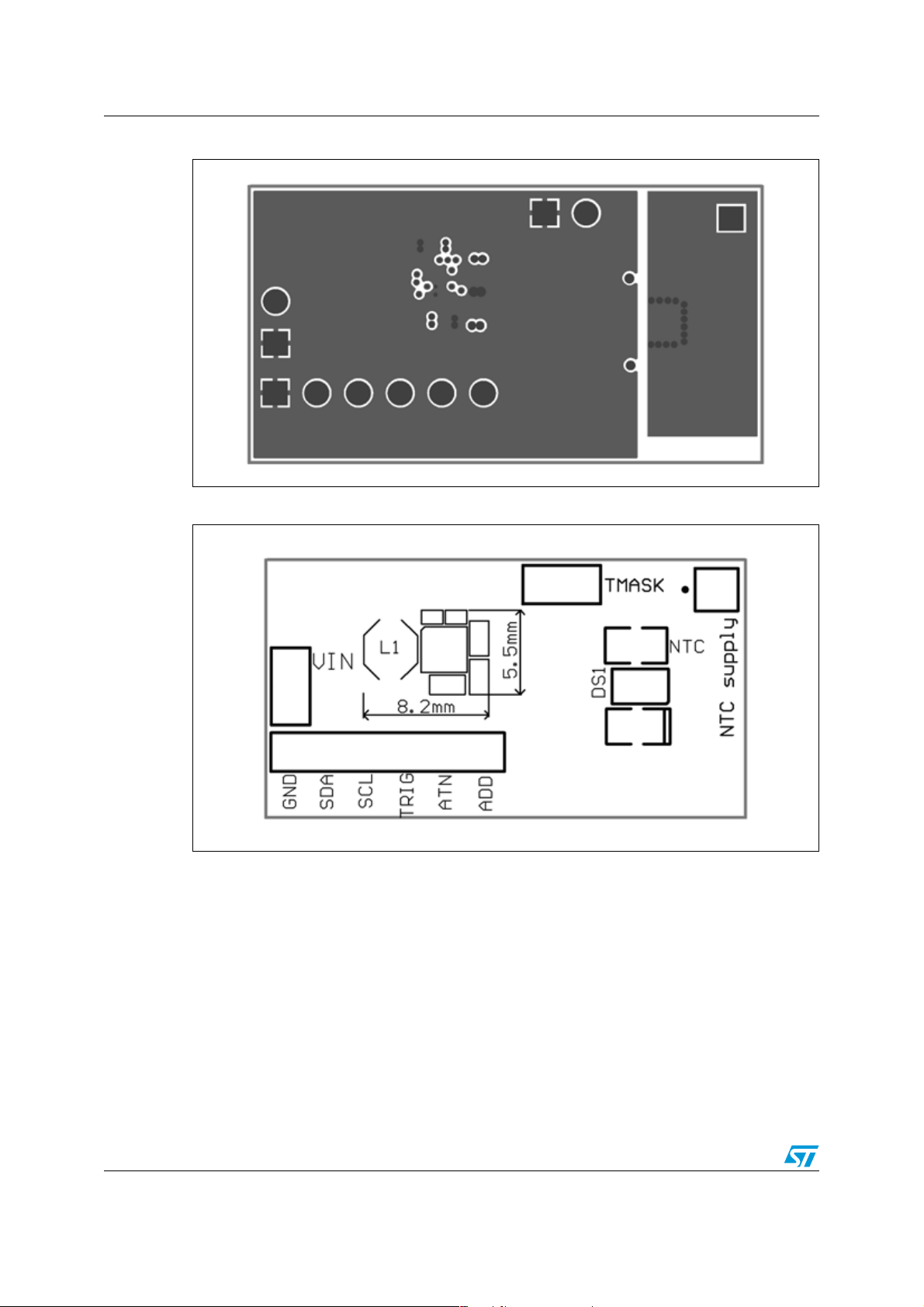
Package and demo board top view
Version B -
Version C
2
C interface. The schematic,
Version A
April 2007 Rev 1 1/31
www.st.com
Page 2

Contents AN2507
Contents
1 Schematic description . . . . . . . . . . . . . . . . . . . . . . . . . . . . . . . . . . . . . . . 6
1.1 Application schematic . . . . . . . . . . . . . . . . . . . . . . . . . . . . . . . . . . . . . . . . . 6
2 Selection of external components . . . . . . . . . . . . . . . . . . . . . . . . . . . . . . 7
2.1 Input and output capacitor selection . . . . . . . . . . . . . . . . . . . . . . . . . . . . . . 7
2.2 Inductor selection . . . . . . . . . . . . . . . . . . . . . . . . . . . . . . . . . . . . . . . . . . . . 7
2.3 LED selection . . . . . . . . . . . . . . . . . . . . . . . . . . . . . . . . . . . . . . . . . . . . . . . 7
2.4 R
2.5 R
2.6 NTC AND R
selection . . . . . . . . . . . . . . . . . . . . . . . . . . . . . . . . . . . . . . . . . . . . . . . 8
FL
selection . . . . . . . . . . . . . . . . . . . . . . . . . . . . . . . . . . . . . . . . . . . . . . . 8
TR
resistor selection . . . . . . . . . . . . . . . . . . . . . . . . . . . . . . . . . 8
X
3 PCB design . . . . . . . . . . . . . . . . . . . . . . . . . . . . . . . . . . . . . . . . . . . . . . . 10
3.1 PCB design rules . . . . . . . . . . . . . . . . . . . . . . . . . . . . . . . . . . . . . . . . . . . 10
3.2 PCB layout . . . . . . . . . . . . . . . . . . . . . . . . . . . . . . . . . . . . . . . . . . . . . . . . 10
3.2.1 A four-layer PCB with application area 45.1 mm2 for BGA package,
version B 10
3.2.2 A two-layer PCB with application area 72.4 mm
3.2.3 A four-layer PCB with application area 45.1 mm
version C 14
2
for QFN package . . . 13
2
for BGA package,
4 Internal registers . . . . . . . . . . . . . . . . . . . . . . . . . . . . . . . . . . . . . . . . . . . 16
4.1 Accessing the internal registers . . . . . . . . . . . . . . . . . . . . . . . . . . . . . . . . 16
5 Operation modes . . . . . . . . . . . . . . . . . . . . . . . . . . . . . . . . . . . . . . . . . . . 17
5.1 SHUTDOWN mode . . . . . . . . . . . . . . . . . . . . . . . . . . . . . . . . . . . . . . . . . 17
5.2 SHUTDOWN mode with the NTC-feature activated . . . . . . . . . . . . . . . . . 17
5.3 READY mode and NTC . . . . . . . . . . . . . . . . . . . . . . . . . . . . . . . . . . . . . . 18
5.4 TORCH mode . . . . . . . . . . . . . . . . . . . . . . . . . . . . . . . . . . . . . . . . . . . . . . 18
5.5 FLASH mode . . . . . . . . . . . . . . . . . . . . . . . . . . . . . . . . . . . . . . . . . . . . . . 19
6 The STATUS register and the ATN pin . . . . . . . . . . . . . . . . . . . . . . . . . . 21
6.1 The STATUS register . . . . . . . . . . . . . . . . . . . . . . . . . . . . . . . . . . . . . . . . 21
7 Reading and writing to the STCF03 registers through the I2C bus . . 22
2/31
Page 3

AN2507 Contents
7.1 Writing to a single register . . . . . . . . . . . . . . . . . . . . . . . . . . . . . . . . . . . . 22
7.2 Writing to multiple registers with incremental addressing . . . . . . . . . . . . 22
7.3 Reading from a single register . . . . . . . . . . . . . . . . . . . . . . . . . . . . . . . . . 23
7.4 Reading from multiple registers with incremental addressing . . . . . . . . . 23
8 Examples of register setup for each mode . . . . . . . . . . . . . . . . . . . . . . 24
8.1 Example 1: 600 mA FLASH with 700 ms duration . . . . . . . . . . . . . . . . . . 24
8.2 Example 2: 25 mA TORCH . . . . . . . . . . . . . . . . . . . . . . . . . . . . . . . . . . . 25
8.3 Example 3: an Auxiliary LED running at 10 mA for 500 ms . . . . . . . . . . . 26
8.4 Example 4: Red-eye reduction (multiple short flashes) . . . . . . . . . . . . . . 27
8.5 Example 5: A FLASH pulse longer than 1.5 s . . . . . . . . . . . . . . . . . . . . . 28
9 Revision history . . . . . . . . . . . . . . . . . . . . . . . . . . . . . . . . . . . . . . . . . . . 30
3/31
Page 4

List of tables AN2507
List of tables
Table 1. Recommended components. . . . . . . . . . . . . . . . . . . . . . . . . . . . . . . . . . . . . . . . . . . . . . . . . 9
Table 2. Accessibility of internal registers. . . . . . . . . . . . . . . . . . . . . . . . . . . . . . . . . . . . . . . . . . . . . 17
Table 3. COMMAND register data to enter SHUTDOWN mode (version B) . . . . . . . . . . . . . . . . . . 17
Table 4. COMMAND register data to enter SHUTDOWN mode (version A and C) . . . . . . . . . . . . . 17
Table 5. COMMAND register data to enter SHUTDOWN mode with NTC activated (version A and C)
18
Table 6. COMMAND register data to enter READY mode . . . . . . . . . . . . . . . . . . . . . . . . . . . . . . . . 18
Table 7. COMMAND register data to enter READY mode with NTC ON. . . . . . . . . . . . . . . . . . . . . 18
Table 8. COMMAND register data to enter TORCH mode. . . . . . . . . . . . . . . . . . . . . . . . . . . . . . . . 19
Table 9. COMMAND register data to enter FLASH mode . . . . . . . . . . . . . . . . . . . . . . . . . . . . . . . . 19
Table 10. STATUS register bits . . . . . . . . . . . . . . . . . . . . . . . . . . . . . . . . . . . . . . . . . . . . . . . . . . . . . 21
Table 11. Effect of the STATUS register bits on the operation of the device . . . . . . . . . . . . . . . . . . . 21
Table 12. TORCH mode and FLASH mode dimming registers settings. . . . . . . . . . . . . . . . . . . . . . . 24
Table 13. COMMAND register data to enter FLASH mode . . . . . . . . . . . . . . . . . . . . . . . . . . . . . . . . 24
Table 14. DIMMING register data for the FLASH mode. . . . . . . . . . . . . . . . . . . . . . . . . . . . . . . . . . . 25
Table 15. I
Table 16. COMMAND register data for the TORCH mode. . . . . . . . . . . . . . . . . . . . . . . . . . . . . . . . . 25
Table 17. DIMMING register data for the TORCH mode . . . . . . . . . . . . . . . . . . . . . . . . . . . . . . . . . . 25
Table 18. I
Table 19. I
Table 20. COMMAND register data for the AUX_LED . . . . . . . . . . . . . . . . . . . . . . . . . . . . . . . . . . . . 26
Table 21. COMMAND register data for the AUX_LED . . . . . . . . . . . . . . . . . . . . . . . . . . . . . . . . . . . . 26
Table 22. I
Table 23. I
Table 24. COMMAND register data for FLASH mode . . . . . . . . . . . . . . . . . . . . . . . . . . . . . . . . . . . . 27
Table 25. DIMMING register data for the FLASH mode. . . . . . . . . . . . . . . . . . . . . . . . . . . . . . . . . . . 27
Table 26. I
Table 27. I
Table 28. 1
Table 29. 2
Table 30. 3
Table 31. Revision history . . . . . . . . . . . . . . . . . . . . . . . . . . . . . . . . . . . . . . . . . . . . . . . . . . . . . . . . . 30
2
C data packet for activating the FLASH mode. . . . . . . . . . . . . . . . . . . . . . . . . . . . . . . . . 25
2
C data packet to activate TORCH mode . . . . . . . . . . . . . . . . . . . . . . . . . . . . . . . . . . . . . 26
2
C data packet for terminating the TORCH mode . . . . . . . . . . . . . . . . . . . . . . . . . . . . . . . 26
2
C data packet for activating the READY mode . . . . . . . . . . . . . . . . . . . . . . . . . . . . . . . . 27
2
C data packet for activating the AUX_LED . . . . . . . . . . . . . . . . . . . . . . . . . . . . . . . . . . . 27
2
C data packet for activating the FLASH mode. . . . . . . . . . . . . . . . . . . . . . . . . . . . . . . . . 28
2
C data packet for activating the FLASH mode. . . . . . . . . . . . . . . . . . . . . . . . . . . . . . . . . 28
st I2
C data packet to restart the FLASH mode . . . . . . . . . . . . . . . . . . . . . . . . . . . . . . . . . 29
nd I2
C data packet for restart of the FLASH mode . . . . . . . . . . . . . . . . . . . . . . . . . . . . . . 29
rd I2
C data packet to restart the FLASH mode . . . . . . . . . . . . . . . . . . . . . . . . . . . . . . . . . 29
4/31
Page 5

AN2507 List of figures
List of figures
Figure 1. A typical application schematic. . . . . . . . . . . . . . . . . . . . . . . . . . . . . . . . . . . . . . . . . . . . . . . 6
Figure 2. NTC connection for versions with internal voltage reference . . . . . . . . . . . . . . . . . . . . . . . . 9
Figure 3. Top layer. . . . . . . . . . . . . . . . . . . . . . . . . . . . . . . . . . . . . . . . . . . . . . . . . . . . . . . . . . . . . . . 10
Figure 4. Middle layer 1 . . . . . . . . . . . . . . . . . . . . . . . . . . . . . . . . . . . . . . . . . . . . . . . . . . . . . . . . . . . 11
Figure 5. Middle layer 2 . . . . . . . . . . . . . . . . . . . . . . . . . . . . . . . . . . . . . . . . . . . . . . . . . . . . . . . . . . . 11
Figure 6. Bottom layer . . . . . . . . . . . . . . . . . . . . . . . . . . . . . . . . . . . . . . . . . . . . . . . . . . . . . . . . . . . . 12
Figure 7. Top overlay. . . . . . . . . . . . . . . . . . . . . . . . . . . . . . . . . . . . . . . . . . . . . . . . . . . . . . . . . . . . . 12
Figure 8. Top layer. . . . . . . . . . . . . . . . . . . . . . . . . . . . . . . . . . . . . . . . . . . . . . . . . . . . . . . . . . . . . . . 13
Figure 9. Bottom layer . . . . . . . . . . . . . . . . . . . . . . . . . . . . . . . . . . . . . . . . . . . . . . . . . . . . . . . . . . . . 13
Figure 10. Top overlay. . . . . . . . . . . . . . . . . . . . . . . . . . . . . . . . . . . . . . . . . . . . . . . . . . . . . . . . . . . . . 14
Figure 11. Top layer. . . . . . . . . . . . . . . . . . . . . . . . . . . . . . . . . . . . . . . . . . . . . . . . . . . . . . . . . . . . . . . 14
Figure 12. Middle layer 1 . . . . . . . . . . . . . . . . . . . . . . . . . . . . . . . . . . . . . . . . . . . . . . . . . . . . . . . . . . . 15
Figure 13. Middle layer 2 . . . . . . . . . . . . . . . . . . . . . . . . . . . . . . . . . . . . . . . . . . . . . . . . . . . . . . . . . . . 15
Figure 14. Bottom layer . . . . . . . . . . . . . . . . . . . . . . . . . . . . . . . . . . . . . . . . . . . . . . . . . . . . . . . . . . . . 16
Figure 15. Top overlay. . . . . . . . . . . . . . . . . . . . . . . . . . . . . . . . . . . . . . . . . . . . . . . . . . . . . . . . . . . . . 16
Figure 16. Splitting the FLASH pulse into several shorter pulses . . . . . . . . . . . . . . . . . . . . . . . . . . . . 20
Figure 17. Writing to a single register . . . . . . . . . . . . . . . . . . . . . . . . . . . . . . . . . . . . . . . . . . . . . . . . . 22
Figure 18. Writing to multiple registers . . . . . . . . . . . . . . . . . . . . . . . . . . . . . . . . . . . . . . . . . . . . . . . . 22
Figure 19. Reading from a single register . . . . . . . . . . . . . . . . . . . . . . . . . . . . . . . . . . . . . . . . . . . . . . 23
Figure 20. Reading from multiple registers . . . . . . . . . . . . . . . . . . . . . . . . . . . . . . . . . . . . . . . . . . . . . 23
Figure 21. Multiple flashes handled by the TRIG pin. . . . . . . . . . . . . . . . . . . . . . . . . . . . . . . . . . . . . . 28
Figure 22. I
2
C bus packets timing for a FLASH lasting longer than FTIM max . . . . . . . . . . . . . . . . . . 30
5/31
Page 6

Schematic description AN2507
1 Schematic description
The FLASH LED driver STCF03 has a high operational frequency (1.8 MHz) which allows
the usage of small-sized external components. The three versions (A, B and C) differ in the
way the NTC feature is supported.
1.1 Application schematic
Figure 1. A typical application schematic
Note: ** Connect to V
Addresses
Note: *** Optional components to support auxiliary functions
● Version A: STCF03PNR - QFN package, external reference for NTC protection
● Version B: STCF03ITBR - BGA package, internal reference for NTC protection
● Version C: STCF03TBR - BGA package, external reference for NTC protection
6/31
, or GND or SDA or SCL to choose one of the 4 different I2C Slave
I
Page 7

AN2507 Selection of external components
2 Selection of external components
2.1 Input and output capacitor selection
It is recommended to use ceramic capacitors with low ESR as input and output capacitors . It
is recommended to use 10 µF/6.3 V as a minimum value of input capacitor and 1 µF/ 6.3 V
as an optimal value of output capacitor to achieve good stability of the device supplied from
low input voltage (2.7 V) at maximum ratings of output power.
Note: see recommended components in Table 1.
2.2 Inductor selection
A thin shielded inductor with a low DC series resistance of winding is recommended f or t his
application. To achieve a good efficiency in step-up mode, it is recommended to use an
inductor with a DC series resistance R
resistance of the LED [Ω, Ω, 1].
For nominal operation, the peak inductor current can be calculated by the following formula:
= RD/10 [Ω, Ω, 1], where RD is the dynamic
DCL
Equation 1
I
PEAK
I
⎛⎞
⎛⎞
----------- -
⎜⎟
⎝⎠
⎝⎠
⎛⎞
OUT
+
⎜⎟
n
⎝⎠
Where:
● I
● I
● n: Efficiency of the STCF03
● V
● V
● L: Inductance value of the inductor
● F: Switching frequency
: Peak inductor current
PEAK
: Current sourced at the VOUT-pin
OUT
: Output voltage at the VOUT-pin
OUT
: Input voltage at the VBAT-pin
IN
Note: see recommended components in Table 1.
2.3 LED selection
All LEDs with a forward voltage range ranging from 2.7 V to 5 V are compatible with
STCF03. The forward voltage spread of any selected LED must however lay within this
range (2.7 V to 5 V). It is possible to set the level of the LED current in FLASH mode and
TORCH mode b y setting the values of the corresponding sensing resistors. The level of the
LED current in FLASH mode can be set by changing the external FLASH resistor.
–()V
V
OUTVIN
---------------------------------------------------- -
2L• F• V
•
IN
2
•
OUT
2
V
OUT
--------------
•=
V
IN
Note: see recommended components in Table 1.
7/31
Page 8

Selection of external components AN2507
2.4 RFL selection
The value of the RFL resistor can be calculated by the following equations:
R
FL = VFB2/IFLASH
where V
power dissipated on the R
= 226 mV and P
FB2
resistor. It is recommended to use a thin metal film resistor with
FL
RFLASH
= R
FL
* I
FLASH
2
, where P
RFL
is the
0805 package size and 1% tolerance. The maximum LED current in FLASH mode for
STCF03 is (800 mA) for a battery voltage ranging from 2.7 V to 5.5 V in VQFPN version.
2.5 RTR selection
The value of the RTR resistor can be calculated by following equations:
Equation 2
V
REFITORCHRFL
⎛⎞
R
--------------------------------------------------------
=
TR
⎝⎠
I
TORCH
•–
and
P
RTORCH
RTRI
•=
2
TORCH
where P
RTORCH
equation R
is the power dissipated on the RTR resistor. It is reco mmended to follow the
= 6.66* RFL to avoid any jump in the current dimming values.
TR
It is recommended to use a thin metal film resistor with 1% or 5% tolerance. The maximum
LED current in TORCH mode f or SCTF03 is 200 mA f or a battery voltage r anging from 2.7 V
to 5.5 V
2.6 NTC AND RX resistor selection
a) A, C versions without an internal reference voltage for the NTC feature.
STCF03 requires a negative thermistor (NTC) for sensing the LED temperature, as w ell as
an R
resistor and an external voltage reference in order to use the NTC feature. Please
X
refer to the typical application schematic in Figure 1 VER A,C for more details.
Once the NTC feature is activated, the internal switch connects the R
and this creates a voltage divider supplied by the external reference voltage connected to
the NTC.
If the temperature of the NTC- thermistor rises due to the heat dissipated by the LED, the
voltage on the NTC pin increases. When this voltage exceeds 0.56 V, the NTC_W bit in the
STATUS register is set to High, and the ATN pin is set to Low to inform the microcontroller
that the LED is becoming hot. The NTC_W bit is cleared by reading the STATUS register.
If the voltage on t he NTC pin rises further and exceeds 1.2 V, the NTC_H bit in the STATUS
register is set to High, and the ATN pin is set to Low to inform the microcontroller that the
LED is too hot and the device goes aut omatically to the READY mode to av oid damaging th e
LED . This status is latched, until the microcontroller reads the STATUS register . Reading the
STATUS register clears the NTC_H bit.
resistor to the NTC,
X
The selection of the NTC and R
resistors values strongl y depend s on the po w er dissip ated
X
by the LED and all components surrounding the NTC-thermistor and on the cooling
capabilities of each specific application. The R
well in the demo board presented in this application note. A real application may require a
different type of NTC-thermistor to achieve optimal thermal protection.
8/31
and the NTC values in Table 1 below work
X
Page 9

AN2507 Selection of external components
The procedure to activate the NTC-feature is described in Section 5.2.
b) Versions with an internal reference voltage fo r the NTC. This version requires a
different connection between the R
and NTC resistors. See Figure 2 below or
X
Figure 1 version B.
Figure 2. NTC connection for versions with internal voltage reference
NTC
STCF03
NTC thermistor
RX
resistor
R
X
To optional A/D converter
Note: Versions with internal reference voltage do not support the SHUTDOWN+NTC mode,
because the internal reference voltage is off in SHUTDOWN mode.
Table 1. Recommended components
Component Manufacturer Part number Value Size
C
I
C
O
L TDK VLF4012AT-4R7M1R1 4.7 µH 3.7 x 3.5 x 1.2 mm
NTC Murata NCP21WF104J03RA 100 kΩ 0805
R
FL
R
TR
R
X
LED Luxeon LED LXCL-PW1
TDK C1608X5R0J106M 10 µF 0603
TDK C1608X5R0J105M 1 µF 0603
Tyco RL73K1JR27JTD 0.27 Ω 0603
Rohm MCR01MZPJ6R20 1.8 Ω 0402
Rohm MCR01MZPJ15K 15 kΩ 0402
9/31
Page 10

PCB design AN2507
3 PCB design
3.1 PCB design rules
STCF03 is a powerful switching device where the PCB must be designed in line with
switched supplies design rules. The po wer tr ac ks (or wires in demo-boar d) must be as short
as possible and wide enough, because of the high currents involved. It is recommended to
use a 4 lay ers PCB to get the best perf o rmance. All e xternal components must be pla ced as
close as possible to STCF03. All high-energ y s witched loo ps should be as small as possib le
to reduce EMI. Most of LEDs need efficient cooling, which could be done by using a
dedicated copper area on the PCB. Please refer to the selected LED's reference guide to
design the heatsink. Place the R
ground pin of the COUT capacitor. In case a modification of any PCB lay er is required, it is
highly recommended to use enough vias. Place the NTC resistor as close as possible to the
LED for good temperature sensing. Direct connection betw een GND and PGND is
necessary in order to achieve correct output current value. No LED current should flow
through this track! Voltage sensing on the R
and directly connected to the R
Pin FB2S must be connected to the R
the copper tracks (if used) must be 0.1 mm in diameter for BGA version. It is recommended
to use the filled vias.
resistor as close as possible to the PGND pins and the
FL
resistor must to done on a trac k from ball FB2
resistor . Again, no current should flow through this track.
FL
FL
resistor pin. Vias connecting the STCF03 pins to
FL
3.2 PCB layout
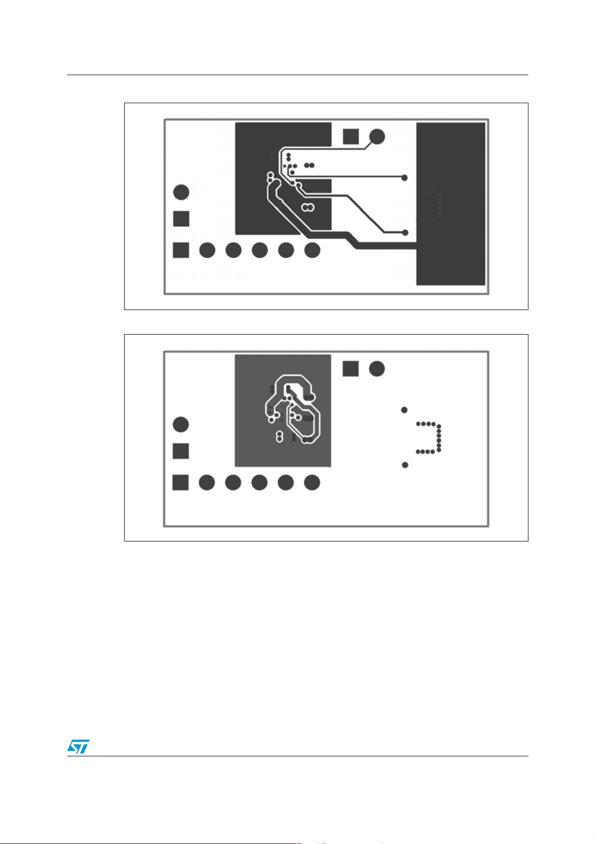
3.2.1 A four-layer PCB with application area 45.1 mm2 for BGA package, version B
(for version C is layout exactly same except the NTC connection, see Figure 1)
Figure 3. Top layer
10/31
Page 11
AN2507 PCB design
Figure 4. Middle layer 1
Figure 5. Middle layer 2
11/31
Page 12

PCB design AN2507
Figure 6. Bottom layer
Figure 7. Top overlay
12/31
Page 13

AN2507 PCB design
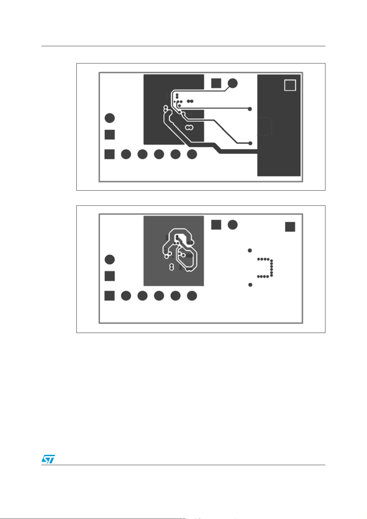
3.2.2 A two-layer PCB with application area 72.4 mm2 for QFN package
Figure 8. Top layer
Figure 9. Bottom layer
13/31
Page 14

PCB design AN2507
Figure 10. Top overlay
3.2.3 A four-layer PCB with application area 45.1 mm2 for BGA package, version C
Figure 11. Top layer
14/31
Page 15
AN2507 PCB design
Figure 12. Middle layer 1
Figure 13. Middle layer 2
15/31
Page 16
Internal registers AN2507
Figure 14. Bottom layer
Figure 15. Top overlay
4 Internal registers
4.1 Accessing the internal registers
There are 4 internal registers in STCF03 (which are the COMMAND, DIMMING, AUX_LED
and STATUS registers). The STATUS register is read-only. The COMMAND register can be
accessed in any operation mode. All the other registers can be accessed in any mode,
except in SHUTDOWN mode. When the device enters SHUTDOWN mode, the DIMMING,
AUX_LED and STATUS registers are cleared. The CO MM AND register value remains
untouched when entering SHUTDOWN mode. Table 2 shows the accessibility of each
register in all operation modes.
16/31
Page 17

AN2507 Operation modes
Table 2. Accessibility of internal registers
Mode
Register Address
SHUTDOWN READY TORCH FLASH
COMMAND 00 Read / Write Read / write Read / write Read / write Untouched Cleared
DIMMING 01 Inaccessible Read / write Read / write Read / write Cleared Cleared
AUX_LED 02 Inaccessible Read / write Read / write Read / write Cleared Cleared
STAT US 03 Inaccessible Read only Read only Read only Cleared Cleared
SHUTDOWN
value
PowerON
reset value
5 Operation modes
5.1 SHUTDOWN mode
SHUTDOWN mode is entered after the Power-ON reset. This mode is mainly used to
decrease the power consumption of the device. During this mode, only the I
alive. The only thing which can be done in SHUTDOWN mode is to access the COMMAND
register. Entering SHUTDOWN mode by wr iting to the COMMAND register aborts any
running operation and clears the v alues of the DIMMING, AUX_LED and STA TUS registers .
The COMMAND register value is not affected b y entering SHUTDOWN mode.
The following data must be written to the COMMAND register to enter SHUTDOWN mode.
2
C interface is
Table 3. COMMAND register data to enter SHUTDO WN mode (version B)
PWR_ON TRIG_EN TCH_ON NTC_ON FTIM_3 FTIM_2 FTIM_1 FTIM_0
CMD_REG
0xxxxx x x
MSB LSB
Table 4. COMMAND register data to enter SHUTDOWN mode (version A and C)
PWR_ON TRIG_EN TCH_ON NTC_ON FTIM_3 FTIM_2 FTIM_1 FTIM_0
CMD_REG
0xx0x x x x
MSB LSB
5.2 SHUTDOWN mode with the NTC-feature activated
This mode is supported only in version A, which does not have any internal voltage
reference for the NTC feature. When this operation mode is activated, the microcontroller
can still monitor the NTC voltage through its A/D converter, while STCF03 remains in
SHUTDOWN mode and therefore saves power.
The following data must be written to the COMMAND register to enter SHUTDOWN mode +
NTC.
17/31
Page 18

Operation modes AN2507
Table 5. COMMAND register data to enter SHUTDOWN mode with NTC activated (version A
and C)
PWR_ON TRIG_EN TCH_ON NTC_ON FTIM_3 FTIM_2 FTIM_1 FTIM_0
CMD_REG
0xx1x x x x
MSB LSB
5.3 READY mode and NTC
The READY mode allows the user to access all the internal registers. The NTC feature can
be activated in this mode and the temperature of the LED can be sensed by the A/D
converter of the microcontroller. The following data must be written to the COMMAND
register to enter READY mode.
Table 6. COMMAND register data to enter READY mode
PWR_ON TRIG_EN TCH_ON NTC_ON FTIM_3 FTIM_2 FTIM_1 FTIM_0
CMD_REG
1000x x x x
MSB LSB
The following data must be written to the COMMAND register to activate the NTC feature .
Table 7. COMMAND register data to enter READY mode with NTC ON
PWR_ON TRIG_EN TCH_ON NTC_ON FTIM_3 FTIM_2 FTIM_1 FTIM_0
CMD_REG
1001x x x x
MSB LSB
As soon as the NTC feature is activ ated, the internal switch conne cts the NTC resistor to the
R
resistor, t her eby creating a voltage divider. The voltage on this divider can be, if desired,
X
monitored by the A/D con verter of the microcontroller . An external v oltage ref erence must be
connected to the NTC to use this feature (only in version A and C). The bits NTC_W and
NTC_H of the STATUS register will not be properly set if there is no external reference
voltage connected to the NTC (only in version A and C).
If the NTC feature is not going to be used, neither the negative thermistor, nor the external
reference needs to be connected. In this case, it is recommended to ground the RX pin. As
the NTC feature is automatically activ ated du ring the FLASH and T ORCH mode , leaving the
RX pin floating could lead to unwanted inter ruptions of the light du e to non- defined voltages
on the RX pin
5.4 TORCH mode
This mode is intended to be used for low light intensities. The LED current in the TORCH
mode can be adjusted in a range from 15 mA up to 200 mA.
The TORCH mode is activated by writing the following data to the COMMAND register.
18/31
Page 19

AN2507 Operation modes
Table 8. COMMAND register data to enter TORCH mode
PWR_ON TRIG_EN TCH_ON NTC_ON FTIM_3 FTIM_2 FTIM_1 FTIM_0
CMD_REG
101xx x x x
MSB LSB
The DIMMING register value (TDIM) must be set as well, unless it has already been set
during a previous operatio n. If TDIM re gister is not se t, then the default output current value
will be at the minimum.
There is no internal timer which controls the TORCH duration. Therefore, as soon as the
TORCH mode is activated, it remains active until a new mode is entered by writing a new
data to the COMMAND register.
If the TORCH mode was terminated by entering READY or FLASH mode, it can be restarted
again by writing the corresponding data to the COMMAND register only, because entering
any of the READY and FLASH modes does not influence the TDIM value. If the TORCH
mode was terminated by ent ering into SHUTDO WN m ode, then the TDI M v alue m ust be set
again during the restart of the TORCH, because entering the SHUTDO WN mod e clears the
TDIM value.
As soon as the TORCH mode is acti vated, the NTC feature is automatically activated too in
order to protect the LED against overheating. The NTC feature will be activated even if the
NTC_ON bit in the COMMAND register is set to zero.
5.5 FLASH mode
This mode is intended to be used for high light intensities. The LED current in the FLASH
mode can be adjusted up to 800 mA with the input v oltage ranging from 3.3 V up to 5.5 V.
The FLASH mode is activated by writing the fo llowing data to the COMMAND register.
Table 9. COMMAND register data to enter FLASH mode
PWR_ON TRIG_EN TCH_ON NTC_ON FTIM_3 FTIM_2 FTIM_1 FTIM_0
CMD_REG
11xxx x x x
MSB LSB
The DIMMING register value (FDIM) must be set as well, unless it has already been set
during a previous operation.
The activation of the FLASH mode requires the TRIG pin to be High. The FLASH mode is
active only when the TRIG_E N bit in the CO MMAND re gister is set to 1 an d th e TRIG pin is
High. This gives the user the possibility to choose between a soft and a hard triggering of
the FLASH mode.
The soft triggering is done by writing data to the internal registers only, while the TRIG pin is
permanently kept High, that is, by connecting it to VBAT. This saves one pin of the
microcontroller, which can be used for a different purpose, but this way of triggering is less
accurate than the hard one. The second disadvantage of this solution is that the FLASH
duration can only be set in discrete steps of the internal timer (1 step = approx. 100 ms).
19/31
Page 20
Operation modes AN2507
Hard-triggering of the FLASH mode requires the microcontroller to manage the TRIG pin.
The COMMAND and the DIMMING registers are loaded with data be f ore the TRIG pin is set
to High. This allows the user to av oi d t he I
2
C-bus latency. FLASH mode then starts as soon
as the TRIG pin is set to High. It takes typically about 0.7 ms to ramp-up the LED current to
the adjusted value. This time may vary according to the LED current value and the battery
voltage. When the TRIG pin is kept High long enough, the internal timer reaches zero and
the FLASH mode is over. As soon as the FLASH is timed out, the ATN pin is pulled down for
11µs to inform the microcontroller that the STATUS register was updated and that the flash
is over . If the TRIG pin is set to Lo w bef ore th e internal timer reaches z ero , the FL ASH mode
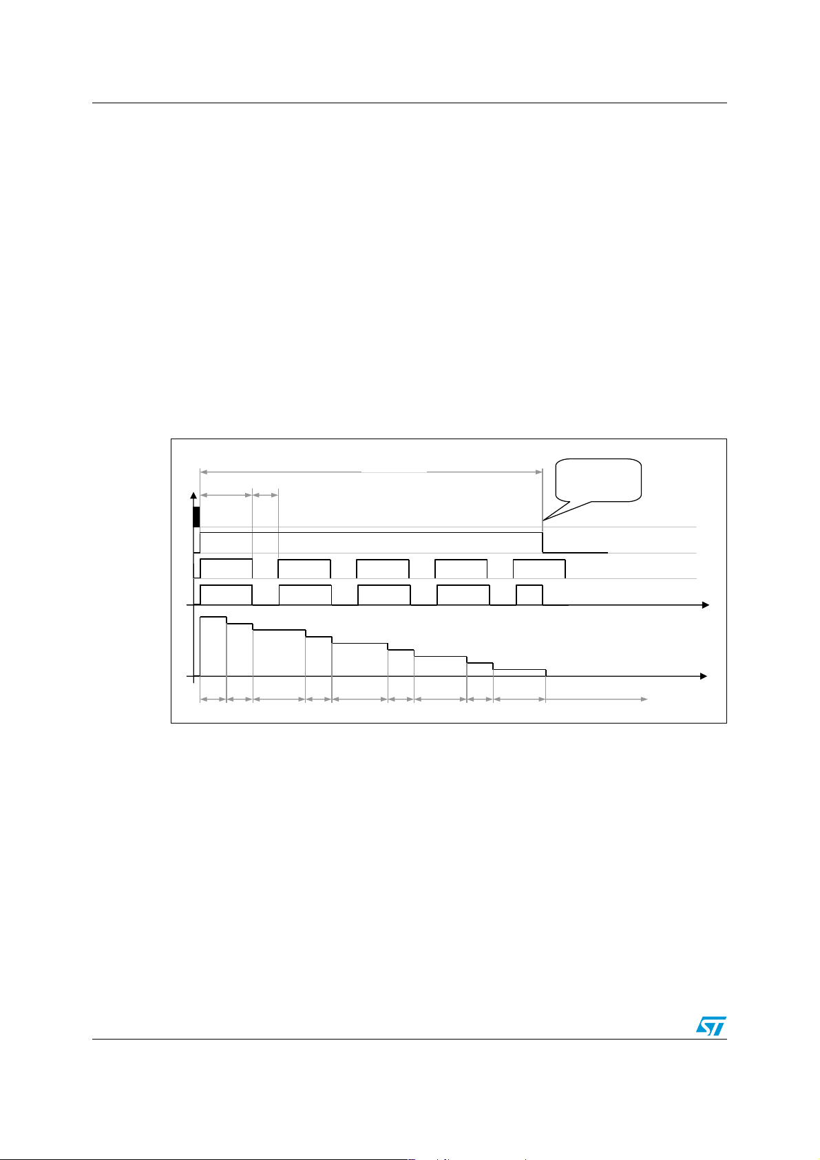
will be interrupted and can be restarted by setting the TRIG pin to High again. The internal
timer is stopped while the TRIG pin is Low. This means that the user can split the FLASH
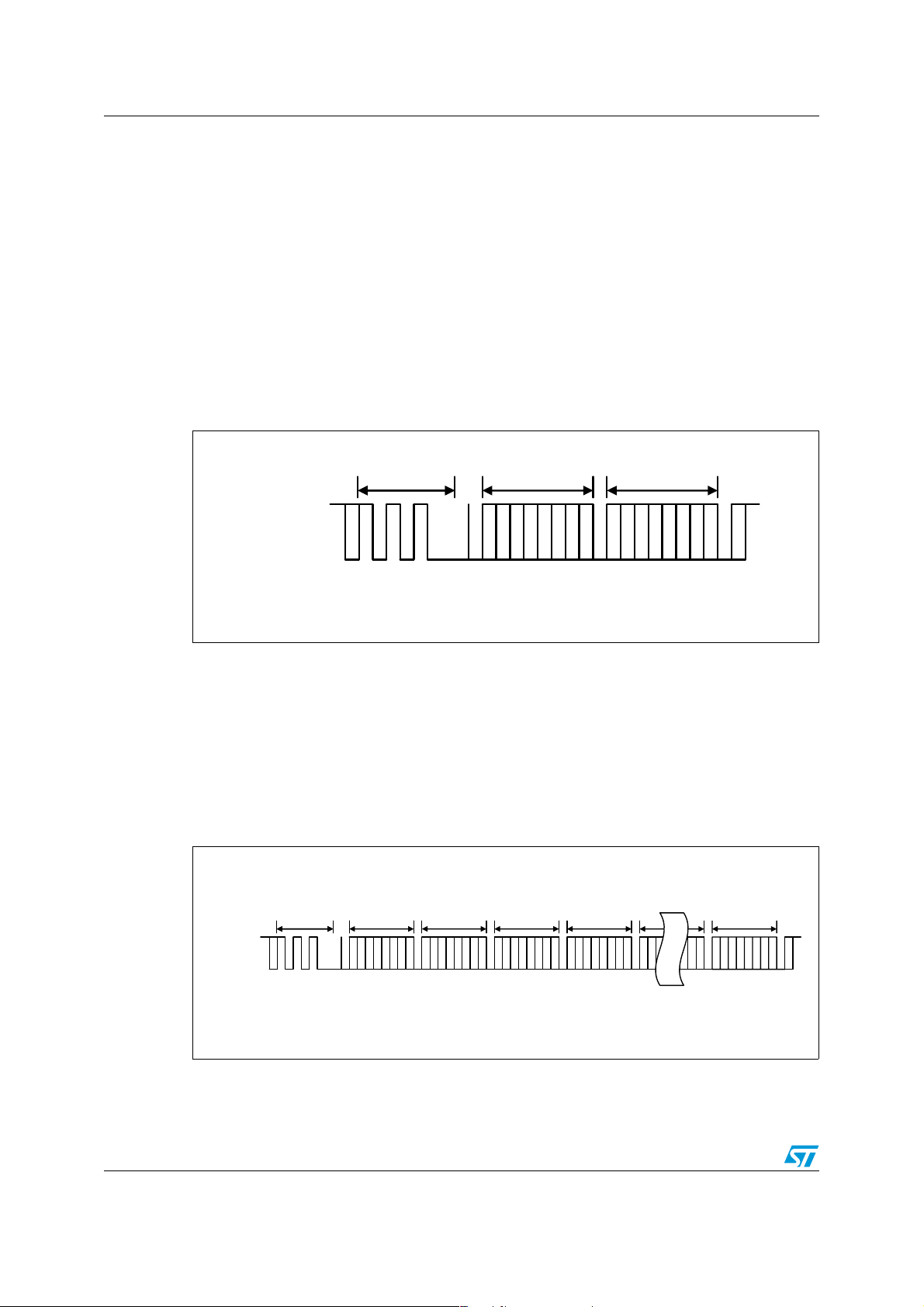
into sever al pulses o f a tota l length equal to the FT IM v alue . Figure 16 below shows splitting
of the FLASH into several shorter pulses. The cumulative length of all the pulses is
determined by the FTIM value. Figure 16 shows the case for FTIM = 9 (900 ms FLASH
time). The cumulative time when the TRIG pin is High is 1000 ms (5 pulses 200 ms long).
The last FLASH pulse will be100ms long only. The reason is that the internal FLASH timer
reaches zero and the TRIG_EN bit is set to 0.
Figure 16. Splitting the FLASH pulse into several shorter pulses
1300 ms
100
200
ms
ms
9 8 7 6 5 4 3 2 1 0
Time when the
internal flash
timer reaches 0
I2C bus packet
TRIG_EN bit
TRIG pin
LED current
Internal Flash timer values
Hard triggering allows therefor e a smooth setting of the FLASH duration. The resolution is
about 8.8µs. The minimum FLASH du ration is limited by the ramp-up time of the LED
current and the maximum is limited by the FTIM value. If it is necessary to make a FLASH
pulse longer than the maximum allowe d by FTIM, then it is necessary to reload the
COMMAND register before the internal timer reaches zero (start a new FLASH before the
previous one elapses). See Section 8.5 - Example 5 for more details.
20/31
Page 21

AN2507 The STATUS register and the ATN pin
6 The STATUS register and the ATN pin
6.1 The STATUS register
Table 10. STATUS register bits
Bit name N/A F_RUN LED_F NTC_W NTC_H OT_F N/A VOUTOK_N
MSB LSB
A detailed description of each bit is stated in the datasheet.
Table 11. Effect of the STATUS register bits on the operation of the device
Bit name
Default value 0 0 0 0 0 0
Latched
Forces READY
mode when set
Sets A TN LOW when
1. YES means that the bit is set by internal signals and is reset to its default value by an I2C-read operation of STAT_REG; NO
means that the bit is set and reset by internal signals in real-time
(1)
set
F_RUN
(STAT_REG)
NO YES YES YES YES YES
NO YES NO YES YES YES
NO YES YES YES YES YES
LED_F
(STAT_REG)
NTC_W
(STAT_REG)
NTC_H
(STAT_REG)
OT_F
(STAT_REG)
VOUTOK_N
(STAT_REG)
When the status register is latched, reading and writing to the registers is still possible, but the bits
TRIG_EN and TCH_ON in the COMMAND register and AUXL register cannot be changed, until the
device is unlatched. It is necessary to read the STATUS register to unlatch the device.
The ATN pin is also pulled down when the internal timer reaches zero in FLASH mode. In this case the
ATN pin is pulled down for 11 µs only. It is recommended to connect the ATN pin to the interrupt input of
the microcontroller. If it is not connected to the interrupt input, the ATN pin should be pulled fast enough
not to miss the 11 µs pulse, that is, by a programming loop which is entered after start of the FLASH
mode. This loop runs until the ATN pin gets Low. It is recommended to make a time-out of such a loop.
21/31
Page 22
Reading and writing to the STCF03 registers through the I2C bus AN2507
7 Reading and writing to the STCF03 registers through
2
the I
7.1 Writing to a single register
Writing to a single register starts with a START-bit followed by the 7-bit device address of
STCF03. The 8-th bit is the R/W bit, which is 0 in this case. R/W = 1 means a Reading
operation. Then the master a w aits an ackno wledgem ent from STCF 03. The 8-b it address o f
the desired register is sent afterwards to STCF03. It will also be followed by an ac knowledge
pulse. The last transmitted byte is the data that is going to be written into the register. It is
followed a gain b y an ac knowled ge pulse from STCF03. Then the master ge nerates a STOPbit and the communication is over. See Figure 17 below.
Figure 17. Writing to a single register
C bus
SDA LINE
DEVICE
ADDRESS
7 bits
S
M
T
S
A
B
R
T
W
R
I
T
E
R
L
/
S
W
B
M
A
C
B
K
ADDRESS OF
S
REGISTER
DATA
A
M
L
A
C
S
S
C
K
B
B
K
L
A
S
S
C
T
O
B
K
P
7.2 Writing to multiple registers with incremental addressing
It would be unpractical to send several times the device address and the address of the
register when writing to multiple registers. STCF03 supports writing to multiple registers with
incremental addressing. When data is written to a register, the register address is
automatically incremented (by one), and therefore the next data can be sent without sending
again the device address and the register address. See Figure 18 below.
Figure 18. Writing to multiple registers
W
DEVICE
R
ADDRESS OF
I
REGISTER i
T
E
R
A
M
L
/
C
S
S
W
K
B
B
DATA i
A
M
A
M
L
C
S
C
S
S
K
B
K
B
B
DATA i+1
M
A
L
S
C
S
B
K
B
DATA i+2
M
A
L
S
C
S
B
K
B
DATA i+2
M
A
L
S
C
S
B
K
B
DATA i+n
M
A
L
S
C
S
B
K
B
SDA LINE
ADDRESS
7 bits
S
M
T
S
A
B
R
T
A
L
S
C
S
T
O
K
B
P
22/31
Page 23

AN2507 Reading and writing to the STCF03 registers through the I2C bus
7.3 Reading from a single register
The reading operation starts with a START-bit followed by 7 bit device address of STCF03.
The 8-th bit is the R/W bit, which is 0 in this case. STCF03 confirms the receiving of the
address + R/W bit by an acknowledge pulse. The address of the register which should be
read is sent after and confirmed by an acknowledge pulse from STCF03 again. Then the
master generates a START-bit again and sends the device address followed by the R/W-bit,
which is 1 now . STCF03 confirms the receiving of the add ress + R/W -bit b y an ac knowledge
pulse, and starts to send data to the master. No acknowledge pulse from the master is
required after receiving the data. Then the master generates a STOP-bit to terminate the
communication. See the Figure 19 below.
Figure 19. Reading from a single register
DEVICE
ADDRESS
7 bits
W
R
T
E
I
ADDRESS OF
REGISTER
DEVICE
ADDRESS
7 bits
R
E
A
D
DATA
SDA LINE
S
M
T
S
A
B
R
T
R
M
L
A
/
S
S
C
W
B
B
K
S
A
L
T
C
S
A
K
B
R
T
A
R
C
/
K
W
S
N
L
T
O
S
O
B
P
A
C
7.4 Reading from multiple registers with incremental addressing
Reading from multiple registers starts in the same wa y as read ing from a single register. As
soon as the first register is read, the register address is automati cally incremented. If the
master generates an ac kn owledge pulse after receiving the da ta from th e f irst r egister, then
reading from the next register can start immediately without having to send once more the
device and the register addresses. The last acknowledge pulse before the STOP-bit is not
required. See Figure 20 below.
Figure 20. Reading from multiple registers
SDA LINE
W
DEVICE
R
ADDRESS
7 bits
S
M
T
S
A
B
R
T
ADDRESS OF
I
REGISTER i
T
E
R
A
M
L
/
C
S
S
W
K
B
B
DEVICE
R
ADDRESS
E
DATA i
A
7 bits
D
S
A
L
T
C
S
A
K
B
R
T
A
R
C
/
K
W
DATA i+1
M
A
L
S
C
S
B
K
B
DATA i+2
A
M
L
C
S
S
K
B
B
DATA i+2
A
L
M
C
S
S
K
B
B
DATA i+n
L
M
A
S
S
C
B
B
K
N
S
L
O
T
S
O
B
A
P
C
K
23/31
Page 24

Examples of register setup for each mode AN2507
8 Examples of register setup for each mode
A device address 0x62 is used in all the example below. The STCF03 is configured to this
device address, if the ADD pin is connected to VBAT
address is 0x60 because the ADD pin is connected to GND.
Table 12. TORCH mode and FLASH mode dimming registers settings
T_DIM
F_DIM
current
Internal
V
Sense
Resist.
0123456789ABCDEF
(hex)
(hex)
LED
16 19 23 27 32 39 46 55 65 77 92 109 124 147 175 209 248 296 352 418 498 592 705 840
[mA]
1 2 3 4 5 6 7 8 9 101112131415161718192021222324
step
REF1
33 40 47 56 67 80 95 113 134 160 190 227 33 40 47 56 67 79 95 113 134 160 190 227
[mV]
R
R
R
R
R
R
FL
FL
FL
FL
+
+
R
TR
+
R
R
TR
TR
FL
+
+
R
R
TR
TR
R
FL
FL
+
+
R
R
TR
TR
0 1 2 345678 9ABCDEF
R
R
R
R
FL
FL
+
R
TR
FL
+
+
R
R
TR
TR
R
FL
FL
+
+
R
TR
RFLRFLRFLRFLRFLRFLRFLRFLRFLRFLRFLR
R
TR
pin. In the demoboard the device
FL
Note: LED current values refer to R
= 0.27 Ohm, RTR = 1.8 Ohm
FL
8.1 Example 1: 600 mA FLASH with 700 ms duration
Let's suppose that RFL = 0.27 Ω. The targeted value of the FLASH current is 600 mA and the
FLASH duration should be 700 ms.
The reference voltage must be set to 160 mV to achieve a 600 mA FLASH current with a
0.27 Ω sensing resistor. The value of FDIM (4 bits) must be set to 0xD to set up the
reference voltage to 160 mV. (See Table 12)
The FLASH duration timer can be set to 100ms up to 1500 ms in 100ms increments. If the
desired FLASH duration is 700 ms the value FTIM (4 bits) must be set to 0x7.
Bit PWR_ON of the command register must be set to 1.
Bit TRIG_EN of the command register must be set to 1.
Bit TCH_ON of the command register must be set to 0.
Bit NTC_ON of the command register can be set to any value, because NTC is
automatically ON when the FLASH mode is active. Setting this bit to 0 will not switch off the
NTC.
Table 13. COMMAND register data to enter FLASH mode
PWR_ON TRIG_EN TCH_ON NTC_ON FTIM_3 FTIM_2 FTIM_1 FTIM_0
CMD_REG
11xx0 1 1 1
MSB LSB
24/31
Page 25

AN2507 Examples of register setup for each mode
Table 14. DIMMING register data for the FLASH mode
TDIM_3 TDIM_2 TDIM_1 TDIM_0 FDIM_3 FDIM_2 FDIM_1 FTIM_0
DIM_REG
00001 1 0 1
MSB LSB
It is necessary to write 4 bytes to STCF03 to make a FLASH.
Table 15. I2C data packet for activating the FLASH mode
Byte Hex Binary Comment
1 62 0 1 1 0 0 0 1 0 Device address + R/W bit
2 00 0 0 0 0 0 0 0 0 Command register address
3 D7 1 1 0 1 0 1 1 1 Data of the command register
4 0D 0 0 0 0 1 1 0 1 Data of the dimming register
8.2 Example 2: 25 mA TORCH
Let's suppose that RFL = 0.27 Ω, RTR = 1.8 Ω and the targeted value of the TORCH current is
25 mA.
The reference voltage must be set to 56 mV to achieve 25 mA in TORCH mode with the
resistor values mentioned abo v e. The v alue of TDIM (4 bits) must be set to 0x3 to set up the
reference voltage to 56 mV.
Bit PWR_ON of the command register must be set to 1.
Bit TRIG_EN of the command register must be set to 0.
Bit TCH_ON of the command register must be set to 0.
Bit NTC_ON of the command register can be set to any value, because NTC is
automatically ON, when TORCH mode is active. Setting this bit to 0 does not switch off the
NTC.
Table 16. COMMAND register data for the TORCH mode
PWR_ON TRIG_EN TCH_ON NTC_ON FTIM_3 FTIM_2 FTIM_1 FTIM_0
CMD_REG
10110 0 0 0
MSB LSB
Table 17. DIMMING register data for the TORCH mode
TDIM_3 TDIM_2 TDIM_1 TDIM_0 FDIM_3 FDIM_2 FDIM_1 FDIM_0
DIM_REG
00110 0 0 0
MSB LSB
25/31
Page 26

Examples of register setup for each mode AN2507
It is necessary to write 4 bytes to the STCF03 to run the TORCH mode.
Table 18. I
Byte Hex Binary Comment
1 62 0 1 1 0 0 0 1 0 Device address + R/W bit
2 00 0 0 0 0 0 0 0 0 Command register address
3 B0 1 0 1 1 0 0 0 0 Data of the command register
4 30 0 0 1 1 0 0 0 0 Data of the dimming register
2
C data packet to activate TORCH mode
The duration of the TORCH mode is "unlimited". TORCH mode is terminated by setting the
TCH_ON bit in the COMMAND register to 0.
Termination of the TORCH mode can be done by wr iting the following data to STCF03.
Table 19. I2C data packet for terminating the TORCH mode
Byte Hex Binary Comment
1 62 0 1 1 0 0 0 1 0 Device address + R/W bit
2 00 0 0 0 0 0 0 0 0 Command register address
3 80 1 0 0 0 0 0 0 0 Data of the command register
This puts the STCF03 into READY mode.
8.3 Example 3: an Auxiliary LED running at 10 mA for 500 ms
STCF03 must be into READY mode (both bits TRIG_EN and TCH_ON are 0) to activate the
Auxiliary LED.
A 10 mA output current is reached when AUXI is set to 0x8.
AUXT must be set to 0x5 to have a 500 ms duration of the Auxiliary LED lighting.
Table 20. COMMAND register data for the AUX_LED
PWR_ON TRIG_EN TCH_ON NTC_ON FTIM_3 FTIM_2 FTIM_1 FTIM_0
CMD_REG
Table 21. COMMAND register data for the AUX_LED
AUX_LED
10000 0 0 0
MSB LSB
AUX_3 AUX_2 AUX_1 AUX_0 AUX_3 AUX_2 AUX_1 AUX_0
10000 1 0 1
MSB LSB
26/31
Page 27

AN2507 Examples of register setup for each mode
Writing the 3 bytes below to STCF03 puts it into READY mode. This can be skipped if it
already is in READY mode.
Table 22. I
Byte Hex Binary Comment
1 62 0 1 1 0 0 0 1 0 Device address + R/W bit
2 00 0 0 0 0 0 0 0 0 Command register address
3 80 1 0 0 0 0 0 0 0 Data of the command register
2
C data packet for activating the READY mode
Writing the following 3 bytes to STCF03 will activate the Auxiliary LED for the desired time.
Table 23. I2C data packet for activating the AUX_LED
Byte Hex Binary Comment
1 62 0 1 1 0 0 0 1 0 Device address + R/W bit
2 02 0 0 0 0 0 0 1 0 Auxiliary LED register address
38510000101
Data of the auxiliary LED
register
8.4 Example 4: Red-eye reduction (multiple short flashes)
There are two ways to mana ge this task. The first one is to use hardware triggering of the
flashes through the TRIG pin. This is the most suitable and recommended solution, as it
reduces the usage of the I
continuously. The second solution is to use the software triggering feature, which means a
periodical reloading of the COMMAND register. This however increases traffic on the I
bus and the flashes can only have length, adjustable in 100 ms increments only.
2
C bus and the length of each FLASH pulse can be adjusted
2
C
Let's suppose that R
= 0.27 Ω and the targeted value of the FLASH current is 600 mA. The
FL
task is to make 5 flashes of 200 ms duration with 100 ms pause between them. The setting
of the reference v oltage is identical to the one in Section 8.1. The FLASH timer (FTIM) is set
to 0xF, which represents 1.5 s.
Table 24. COMMAND register data for FLASH mode
PWR_ON TRIG_EN TCH_ON NTC_ON FTIM_3 FTIM_2 FTIM_1 FTIM_0
CMD_REG
11011 1 1 1
MSB LSB
Table 25. DIMMING register data for the FLASH mode
TDIM_3 TDIM_2 TDIM_1 TDIM_0 FDIM_3 FDIM_2 FDIM_1 FDIM_0
DIM_REG
00001 1 0 1
MSB LSB
27/31
Page 28

Examples of register setup for each mode AN2507
The data packet which has to be sent is in the table below.
Table 26. I2C data packet for activating the FLASH mode
Byte Hex Binary Comment
1 62 0 1 1 0 0 0 1 0 Device address + R/W bit
2 00 0 0 0 0 0 0 0 0 Command register address
3 DF 1 1 0 1 1 1 1 1 Data of the command register
4 0D 0 0 0 0 1 1 0 1 Data of the dimming register
The picture below shows the TRIG pin and t he I
2
C bus timings.
Figure 21. Multiple flashes handled by the TRIG pin
100
200
ms
ms
1400 ms
8.5 Example 5: A FLASH pulse longer than 1.5 s
Let's suppose that RFL = 0.27 Ω and the targeted value of the FLASH current is 600 mA. The
task is to make a single FLASH pulse with a 4 seconds duration.
It is necessary to reload FTIM in the COMMAND REGISTER before the internal FLASH
timer reaches zero . This guar antees that the FLASH do es go on and does not stop after
1.5 sec.
The first packet must contain also the DIMMING REGISTER data, if they are different from
those which were used in the previous operation.
● Packet 1
I2C bus packet
TRIG_EN bit
TRIG pin
Sets FLASH mode with 1.5 s duration and the proper dimming.
Table 27. I2C data packet for activating the FLASH mode
Byte Hex Binary Comment
1 62 0 1 1 0 0 0 1 0 Device address + R/W bit
2 00 0 0 0 0 0 0 0 0 Command register address
3 DF 1 1 0 1 1 1 1 1 Data of the command register
4 0D 0 0 0 0 1 1 0 1 Data of the dimming register
28/31
Page 29

AN2507 Examples of register setup for each mode
● Packet 2
Sets FLASH mode with 1.5 s duration. Dimming is not set again as it is same as before.
Table 28. 1
Byte Hex Binary Comment
1 62 0 1 1 0 0 0 1 0 Device address + R/W bit
2 00 0 0 0 0 0 0 0 0 Command register address
3 DF 1 1 0 1 1 1 1 1 Data of the command register
● Packet 3
st I2
C data packet to restart the FLASH mode
Sets FLASH mode with 1.5 s duration. Dimming remains untouched.
Table 29. 2
Byte Hex Binary Comment
1 62 0 1 1 0 0 0 1 0 Device address + R/W bit
2 00 0 0 0 0 0 0 0 0 Command register address
3 DF 1 1 0 1 1 1 1 1 Data of the command register
● Packet 4
nd I2
C data packet for restart of the FLASH mode
Sets FLASH mode with 1 s duration. Dimming remains untouched.
Table 30. 3
rd I2
C data packet to restart the FLASH mode
Byte Hex Binary Comment
1 62 0 1 1 0 0 0 1 0 Device address + R/W bit
2 00 0 0 0 0 0 0 0 0 Command register address
3 DA 1 1 0 1 1 0 1 0 Data of the command register
Please refer to Figure 22 for more details about the I
2
C-bus packe ts timing.
The solution described above is using a software termination of the FLASH pulse. (It is
timed out by the internal timer.) The FLASH pulse could be also terminated by setting the
TRIG pin to low after 4 seconds. In this case, the fourth packet could be the same as
packets Pac ket 2 and Packet 3, because the timing of the FLASH is done by the TRIG pin
and it is not necessary to change the value of FTIM in the COMMAND REGISTER.
This way of periodical reloading of the COMMAND REGISTER ca n be used to achieve a
continuous FLASH light. In this case, it is very strongly recommended to guarantee an
efficient cooling of both the LED and the chip, otherwise the light can be interrupted by
activation of the thermal protections.
29/31
Page 30

Revision history AN2507
p
Figure 22. I2C bus packets timing for a FLASH lasting longer than FTIM max
Timeout of the
first Flash
1.5s
1.0s 1.0s 1.0s 1.0s
Timeout of the
second Flash
1.5s
4.0s
9 Revision history
Table 31. Revision history
Date Revision Changes
Timeout of the
third Flash
1.5s
1.0s
Timeout of the
fourth Flash –
ending of the
whole Flash
ulse
I2C bus packets
TRIG_EN bit
TRIG pin
19-Apr-2007 1 Initial release
30/31
Page 31

AN2507
Please Read Carefully:
Information in this document is provided solely in connection with ST products. STMicroelectronics NV and its subsidiaries (“ST”) reserve the
right to make changes, corrections, modifications or improvements, to this document, and the products and services described herein at any
time, without notice.
All ST products are sold pursuant to ST’s terms and conditions of sale.
Purchasers are solely res ponsibl e fo r the c hoic e, se lecti on an d use o f the S T prod ucts and s ervi ces d escr ibed he rein , and ST as sumes no
liability whatsoever relati ng to the choice, selection or use of the ST products and services described herein.
No license, express or implied, by estoppel or otherwise, to any intellectual property rights is granted under this document. If any part of this
document refers to any third pa rty p ro duc ts or se rv ices it sh all n ot be deem ed a lice ns e gr ant by ST fo r t he use of su ch thi r d party products
or services, or any intellectua l property c ontained the rein or consi dered as a warr anty coverin g the use in any manner whats oever of suc h
third party products or servi ces or any intellectual property contained therein.
UNLESS OTHERWISE SET FORTH IN ST’S TERMS AND CONDITIONS OF SALE ST DISCLAIMS ANY EXPRESS OR IMPLIED
WARRANTY WITH RESPECT TO THE USE AND/OR SALE OF ST PRODUCTS INCLUDING WITHOUT LIMITATION IMPLIED
WARRANTIES OF MERCHANTABILITY, FITNESS FOR A PARTICUL AR PURPOS E (AND THEIR EQUIVALE NTS UNDER THE LAWS
OF ANY JURISDICTION), OR INFRINGEMENT OF ANY PATENT, COPYRIGHT OR OTHER INTELLECTUAL PROPERTY RIGHT.
UNLESS EXPRESSLY APPROVED IN WRITING BY AN AUTHORIZED ST REPRESENTATIVE, ST PRODUCTS ARE NOT
RECOMMENDED, AUTHORIZED OR WARRANTED FOR USE IN MILITARY, AIR CRAFT, SPACE, LIFE SAVING, OR LIFE SUSTAINING
APPLICATIONS, NOR IN PRODUCTS OR SYSTEMS WHERE FAILURE OR MALFUNCTION MAY RESULT IN PERSONAL INJ URY,
DEATH, OR SEVERE PROPERTY OR ENVIRONMENTAL DAMAGE. ST PRODUCTS WHICH ARE NOT SPECIFIED AS "AUTOMOTIVE
GRADE" MAY ONLY BE USED IN AUTOMOTIVE APPLICATIONS AT USER’S OWN RISK.
Resale of ST products with provisions different from the statements and/or technical features set forth in this document shall immediately void
any warranty granted by ST fo r the ST pro duct or serv ice describe d herein and shall not cr eate or exten d in any manne r whatsoever , any
liability of ST.
ST and the ST logo are trademarks or registered trademarks of ST in various countr ies.
Information in this document su persedes and replaces all information previously supplied.
The ST logo is a registered trademark of STMicroelectronics. All other names are the property of their respective owners.
© 2007 STMicroelectronics - All rights reserved
STMicroelectronics group of compan ie s
Australia - Belgium - Brazil - Canada - China - Czech Republic - Finland - France - Germany - Hong Kong - India - Israel - Italy - Japan -
Malaysia - Malta - Morocco - Singapore - Spain - Sweden - Switzerland - United Kingdom - United States of America
www.st.com
31/31
 Loading...