

Page 1

AN2503
Application note
PDP Power Devices
Introduction
This application note discusses how to select o ptimal po we r de vices a nd contro l circuitry fo r
alternating plasma display panel applications, concentrating on power circuits used to
sustain plasma discharge on the panel.
Plasma Display Panels (PDP) are emerging as the leading candidate for large area wallhanging color TVs and HDTVs [1.]. Its large scr een, wide viewing angle, and thinness have
given it the edge over conventional displays. Scan, Energy Recovery (ERC) and Sustain
(discharge) circuits are important blocks that fulfill important energy saving requirements.
May 2007 Rev 1 1/30
www.st.com
Page 2

Contents AN2503
Contents
1 PDP Module structure . . . . . . . . . . . . . . . . . . . . . . . . . . . . . . . . . . . . . . . . 4
2 PDP basic . . . . . . . . . . . . . . . . . . . . . . . . . . . . . . . . . . . . . . . . . . . . . . . . . . 5
2.1 PDP cell structure . . . . . . . . . . . . . . . . . . . . . . . . . . . . . . . . . . . . . . . . . . . 5
2.2 Panel memory characteristic . . . . . . . . . . . . . . . . . . . . . . . . . . . . . . . . . . . 6
2.3 PDP driving sequence . . . . . . . . . . . . . . . . . . . . . . . . . . . . . . . . . . . . . . . . 8
3 PDP Sustain circuit . . . . . . . . . . . . . . . . . . . . . . . . . . . . . . . . . . . . . . . . . . 9
3.1 Sustain circuit operations . . . . . . . . . . . . . . . . . . . . . . . . . . . . . . . . . . . . . 12
3.1.1 Positive pulse of Vyx . . . . . . . . . . . . . . . . . . . . . . . . . . . . . . . . . . . . . . . 12
3.1.2 Positive discharge and clamping phase . . . . . . . . . . . . . . . . . . . . . . . . . 13
3.1.3 Vyx back to zero . . . . . . . . . . . . . . . . . . . . . . . . . . . . . . . . . . . . . . . . . . 14
3.1.4 Clamping to ground . . . . . . . . . . . . . . . . . . . . . . . . . . . . . . . . . . . . . . . . 14
3.2 Symmetrical Y - X phase . . . . . . . . . . . . . . . . . . . . . . . . . . . . . . . . . . . . . 15
3.3 Reset phase . . . . . . . . . . . . . . . . . . . . . . . . . . . . . . . . . . . . . . . . . . . . . . . 16
4 PDP Power Devices characteristics . . . . . . . . . . . . . . . . . . . . . . . . . . . 17
4.1 Power devices from ST . . . . . . . . . . . . . . . . . . . . . . . . . . . . . . . . . . . . . . 17
4.1.1 Measurement set-up . . . . . . . . . . . . . . . . . . . . . . . . . . . . . . . . . . . . . . . 18
4.1.2 Energy recovery section . . . . . . . . . . . . . . . . . . . . . . . . . . . . . . . . . . . . 19
4.1.3 Discharge section . . . . . . . . . . . . . . . . . . . . . . . . . . . . . . . . . . . . . . . . . 20
4.1.4 Path section . . . . . . . . . . . . . . . . . . . . . . . . . . . . . . . . . . . . . . . . . . . . . . 20
4.1.5 Set - reset section . . . . . . . . . . . . . . . . . . . . . . . . . . . . . . . . . . . . . . . . . 21
4.2 Driving section . . . . . . . . . . . . . . . . . . . . . . . . . . . . . . . . . . . . . . . . . . . . . 22
4.3 Gate driver devices . . . . . . . . . . . . . . . . . . . . . . . . . . . . . . . . . . . . . . . . . 22
4.3.1 Totem pole . . . . . . . . . . . . . . . . . . . . . . . . . . . . . . . . . . . . . . . . . . . . . . . 23
4.4 Input buffer section . . . . . . . . . . . . . . . . . . . . . . . . . . . . . . . . . . . . . . . . . . 24
5 Bill of material and schematics . . . . . . . . . . . . . . . . . . . . . . . . . . . . . . . 25
6 Conclusions . . . . . . . . . . . . . . . . . . . . . . . . . . . . . . . . . . . . . . . . . . . . . . . 28
7 References . . . . . . . . . . . . . . . . . . . . . . . . . . . . . . . . . . . . . . . . . . . . . . . . 28
8 Revision history . . . . . . . . . . . . . . . . . . . . . . . . . . . . . . . . . . . . . . . . . . . 29
2/30
Page 3

AN2503 List of figures
List of figures
Figure 1. PDP module structure. . . . . . . . . . . . . . . . . . . . . . . . . . . . . . . . . . . . . . . . . . . . . . . . . . . . . . 4
Figure 2. Cell structure. . . . . . . . . . . . . . . . . . . . . . . . . . . . . . . . . . . . . . . . . . . . . . . . . . . . . . . . . . . . . 5
Figure 3. Memory effect - no charges . . . . . . . . . . . . . . . . . . . . . . . . . . . . . . . . . . . . . . . . . . . . . . . . . 6
Figure 4. Memory effect - address phase . . . . . . . . . . . . . . . . . . . . . . . . . . . . . . . . . . . . . . . . . . . . . . 6
Figure 5. Memory effect - Wall charges deposit . . . . . . . . . . . . . . . . . . . . . . . . . . . . . . . . . . . . . . . . . 6
Figure 6. Memory effect - discharge . . . . . . . . . . . . . . . . . . . . . . . . . . . . . . . . . . . . . . . . . . . . . . . . . . 7
Figure 7. Memory effect - wall charges deposit . . . . . . . . . . . . . . . . . . . . . . . . . . . . . . . . . . . . . . . . . . 7
Figure 8. Memory effect - discharge with reverse polarity . . . . . . . . . . . . . . . . . . . . . . . . . . . . . . . . . . 7
Figure 9. Subfield structure . . . . . . . . . . . . . . . . . . . . . . . . . . . . . . . . . . . . . . . . . . . . . . . . . . . . . . . . . 8
Figure 10. Subfield structure – expression of gray level . . . . . . . . . . . . . . . . . . . . . . . . . . . . . . . . . . . . 9
Figure 11. Sustain circuit . . . . . . . . . . . . . . . . . . . . . . . . . . . . . . . . . . . . . . . . . . . . . . . . . . . . . . . . . . . 10
Figure 12. Circuit scheme . . . . . . . . . . . . . . . . . . . . . . . . . . . . . . . . . . . . . . . . . . . . . . . . . . . . . . . . . . 11
Figure 13. Circuit scheme – positive pulse of V
Figure 14. Equivalent circuit. . . . . . . . . . . . . . . . . . . . . . . . . . . . . . . . . . . . . . . . . . . . . . . . . . . . . . . . . 12
Figure 15. Circuit scheme – positive discharge and clamping. . . . . . . . . . . . . . . . . . . . . . . . . . . . . . . 13
Figure 16. Circuit scheme – V
back to zero . . . . . . . . . . . . . . . . . . . . . . . . . . . . . . . . . . . . . . . . . . . 14
yx
Figure 17. Circuit scheme – clamping to ground . . . . . . . . . . . . . . . . . . . . . . . . . . . . . . . . . . . . . . . . . 15
Figure 18. Circuit scheme – negative pulse of V
Figure 19. Circuit scheme – negative discharge and clamping . . . . . . . . . . . . . . . . . . . . . . . . . . . . . . 15
Figure 20. Circuit scheme – V
back to zero . . . . . . . . . . . . . . . . . . . . . . . . . . . . . . . . . . . . . . . . . . . 16
yx
Figure 21. Circuit scheme – clamping to ground . . . . . . . . . . . . . . . . . . . . . . . . . . . . . . . . . . . . . . . . . 16
Figure 22. Circuit scheme – set and reset . . . . . . . . . . . . . . . . . . . . . . . . . . . . . . . . . . . . . . . . . . . . . . 17
Figure 23. Inductor current. . . . . . . . . . . . . . . . . . . . . . . . . . . . . . . . . . . . . . . . . . . . . . . . . . . . . . . . . . 19
Figure 24. Gate driver topology with L6385. . . . . . . . . . . . . . . . . . . . . . . . . . . . . . . . . . . . . . . . . . . . . 23
Figure 25. Gate driver topology – L6388 . . . . . . . . . . . . . . . . . . . . . . . . . . . . . . . . . . . . . . . . . . . . . . . 23
Figure 26. STS01DTP06 Totem pole. . . . . . . . . . . . . . . . . . . . . . . . . . . . . . . . . . . . . . . . . . . . . . . . . . 24
Figure 27. Board schematic 1 . . . . . . . . . . . . . . . . . . . . . . . . . . . . . . . . . . . . . . . . . . . . . . . . . . . . . . . 26
Figure 28. Board schematic 2 . . . . . . . . . . . . . . . . . . . . . . . . . . . . . . . . . . . . . . . . . . . . . . . . . . . . . . . 27
. . . . . . . . . . . . . . . . . . . . . . . . . . . . . . . . . . . . . . . . 12
yx
. . . . . . . . . . . . . . . . . . . . . . . . . . . . . . . . . . . . . . . . 15
yx
3/30
Page 4
PDP Module structure AN2503
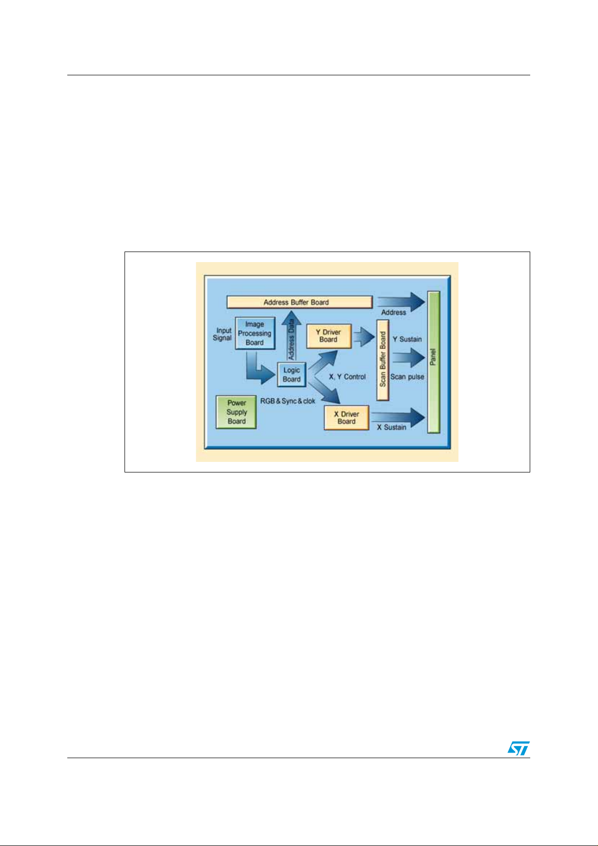
1 PDP Module structure
Po wer supply, address buffer, logic and scan buff er boards are the fundamental blocks of a
PDP. In particular, the energy recovery and sustain function are performed by the Y and X
drive boards. Power MOSFETs, IGBTs, Diodes and Drivers are key products for ERC and
sustain both in X and in Y drive boards. These products are also used for the path, set-reset
function in the Y drive board only. Path switches are mandatory to isolate ERC and Sustain
switches from the negative voltage applied to the display during the scan phase, while, set
and reset switches determine identical initial condition of the plasma cells before each
address cycle.
Figure 1. PDP module structure
ST's extensive portfolio covers the whole solutio n for an energy recovery circuit (ERC),
sustain circuit, path circuit, and set-reset circuit, both from a power device and IC driver
perspective.
The ST solution takes into account all fundamental requirements like cost, component
count, reliability and power consumption.
Reduced power losses and higher switching frequency are the main benefits of ST's
advanced technology.
4/30
Page 5
AN2503 PDP basic
2 PDP basic
Basic knowledge on Plasma Display Panel encompasses manufacturing issues in cell
structure, physics principle in the memo ry effect, and display algorithms needed to create a
range of colors.
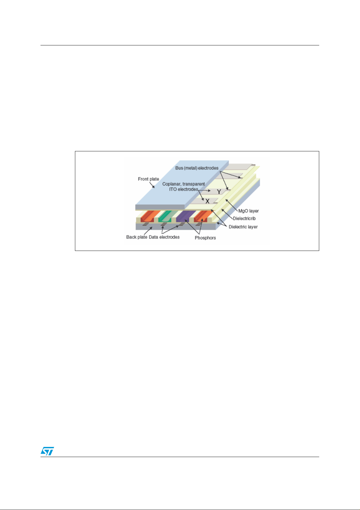
2.1 PDP cell structure
Figure 2 shows the structure of a plasma display glass panel, [2.].
Figure 2. Cell structure
An AC PDP displa y is composed of front and rear glass substrates sandwiche d together and
then sealed. The air is vacuumed out and a mixture of inert gases (Ne and Xe) is injected
between the glass substrates . The separation between the two opp osing substrates is about
100um and the space between them is filled with a gas mixture of Ne and Xe. The front
glass substrate has a first electrode (X electrode) and a second electrode (Y electrode)
which operate as sustain electrodes. The X and Y electrodes are coated with bus
electrodes, dielectric layer, and MgO layer in sequence. The MgO protects the dielectric
from plasma damage and also aids the plasma in sustaini ng a discharge through secondary
electron emission from its surface. In addition, equivalent capacitor exists between the X
and Y electrodes. On the surface of the rear glass substrate, as opposed to the front glass
substrate, a third electrode operating as an address electrode (A electrode) is formed to be
orthogonal to the X and Y electrodes. Electrically, the entire assembly can now be
considered as a three-electrode capacitor. A cross point is formed where the X, Y and A
electrodes meet. Three adjacent red, blue and green cross points form a color picture
element (pixel) of the panel. In operation, an AC voltage sufficiently high will ionize the gas
to create the plasma. Then, the ultraviolet light from the plasma excites the phosphor to
create the color image.
Each pixel can be independently controlled and can assume different color gradations. The
number of pixels available determines the resolution of the glass panel vertically and
horizontally.
5/30
Page 6
PDP basic AN2503
3
3
2.2 Panel memory characteristic
The AC PDPs provide inheren t memory characteristics [3.], [4.], as explained in the
following figures.
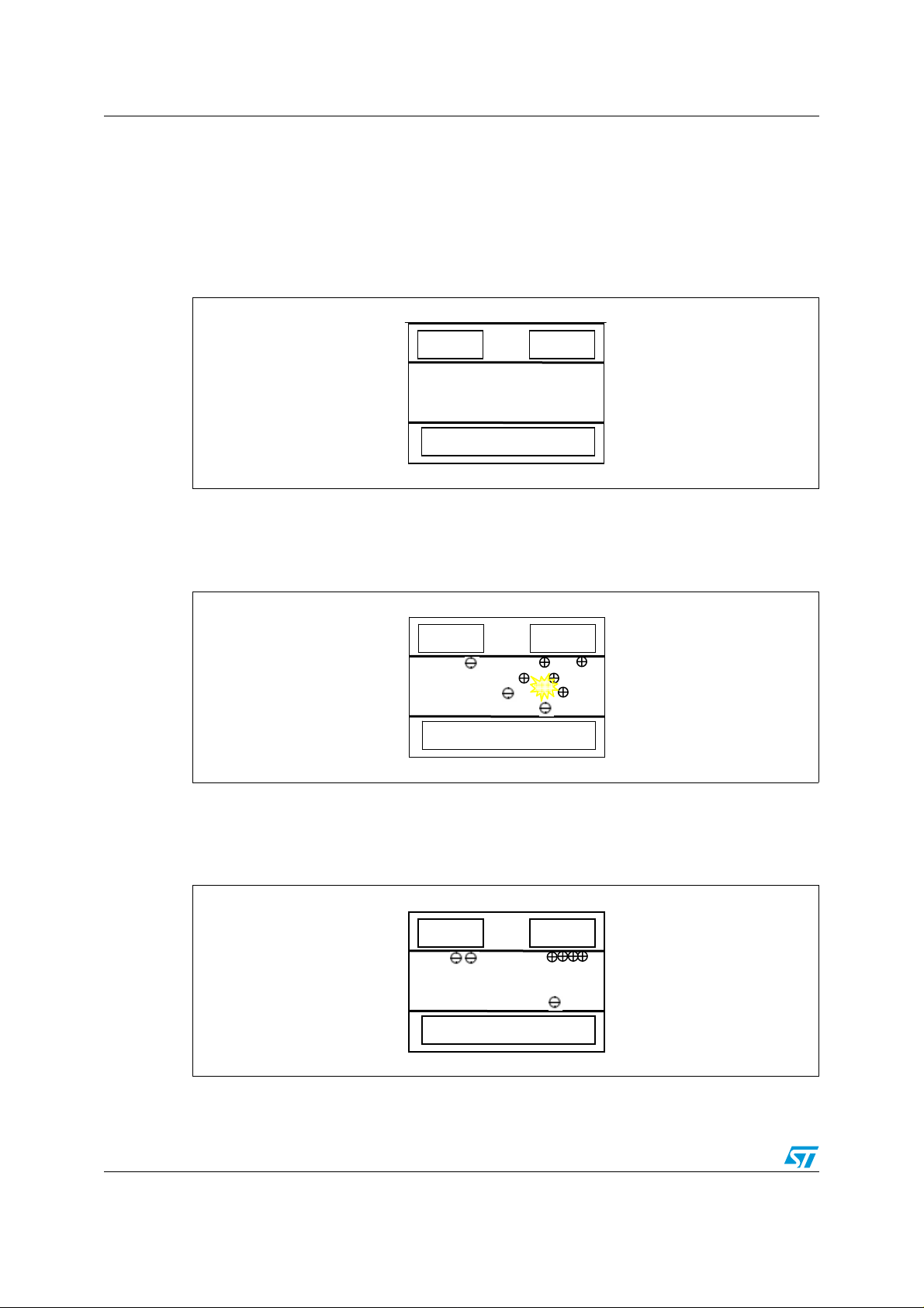
In general, the AC sustain square pulse voltage (V
), whose voltage Vs is smaller than the
xy
gas breakdown voltage Vbd, cannot initiate a discharge, as shown in Figure 3.
Figure 3. Memory effect - no charges
X = Vs Y = GND
Address = Vs/2
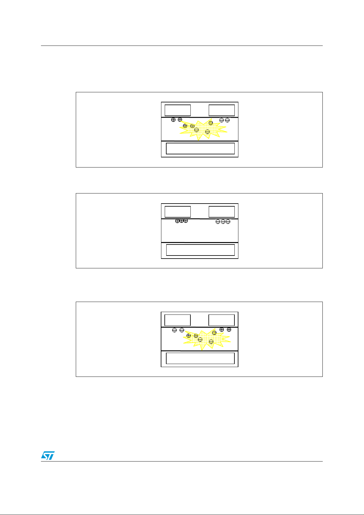
If data pulses Vd are applied to the address electrodes, while scan pulses -Vy are
sequentially applied to each Y electrode, the voltage (Vd + Vy) is higher than Vbd and a
weak discharge ignites, as shown in Figure 4.
Figure 4. Memory effect - address phase
X = Vk Y = -Vy
Charges, called wall charges (or w all voltage Vw), deposit on the dielectric lay er and reduce
the effective voltage across the gap. Then, the discharge ceases after a short time, as
shown in Figure 5.
Figure 5. Memory effect - Wall charges deposit
X = Vk Y = -Vy
6/30
Address = Vd
Address = Vd
Page 7
AN2503 PDP basic
3
When the polarity of the sustain pulse is reversed, the potential difference across the gap
becomes larger than Vbd by an amou nt determined by the wall charges, and a new large
discharge of different polarity occurs, as shown in Figure 6.
Figure 6. Memory effect - discharge
X = GND Y = Vs
Address = Vs/2
The build-up of wall charges again terminates the discharge, as shown in Figure 7.
Figure 7. Memory effect - wall charges deposit
X = GND Y = Vs
Address = Vs/2
The next discharge starts as the polarity of the sustain pulse is reversed, as shown in
Figure 8.
Figure 8. Memory effect - discharge with reverse polarity
X = Vs Y = GND
Address = Vs/2
Once the discharge is initiated, it continues as long as the sustain pulse is applied. Due to
this memory characteristic of AC PDPs, lower sustain voltage (< Vbd) pulses can maintain
the ac PDPs to light.
In other words, the p rocess of panel image d ispla ying depends on a f ormer process of panel
addressing. In fact, during the address phase a small amount of charges (wall charges)
deposit on the selected electrodes without any visible light emission. This reduces the
7/30
Page 8
PDP basic AN2503
threshold voltage for discharge, and consequently, during sustain phase only selected cells
ignite and emit light.
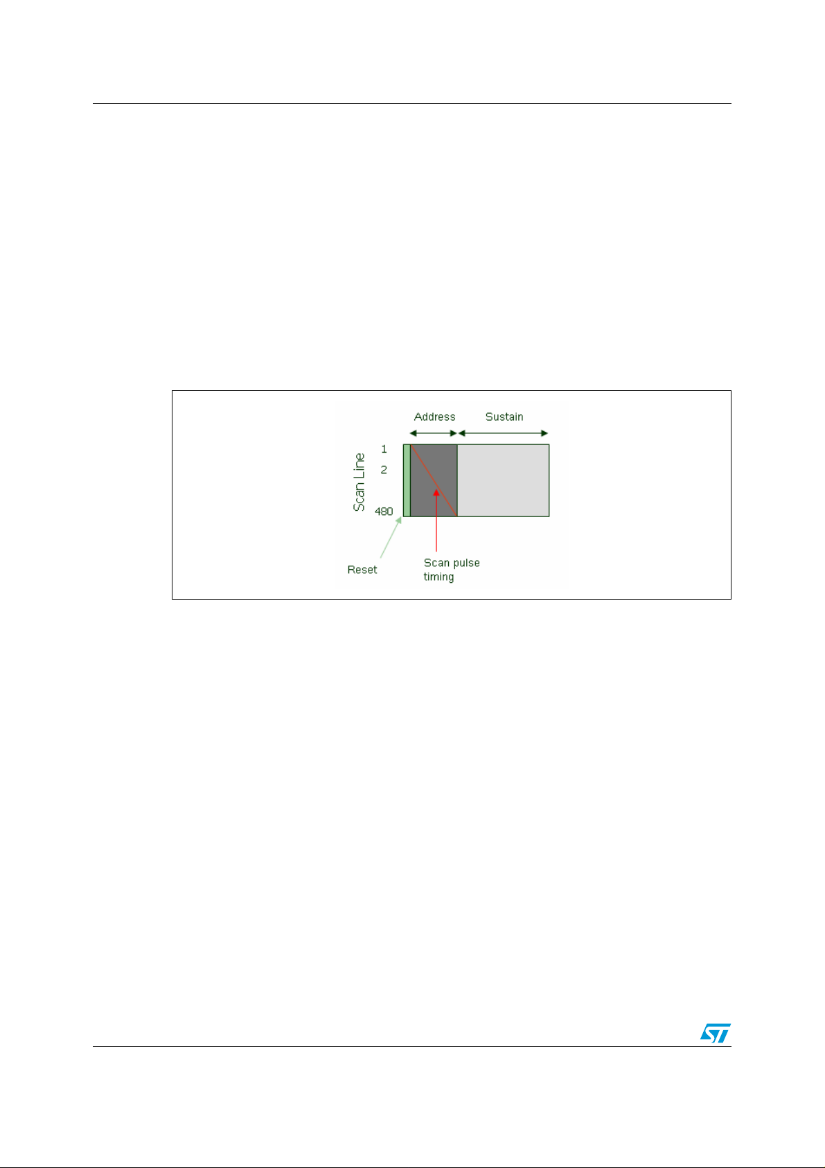
2.3 PDP driving sequence
The most common method of displaying one picture field is using the Address DisplaySeparation method (ASD).
All X electrodes are bused together and connected to a sustain driver, while the Y
electrodes are connected to susta in driver through seve ral scan ICs. One TV field is divided
into 10 subfields (SFs) in a 10-bit codification case, and each consists of a reset period, an
address period, and a display period (Figure 9).
On every subfield, each cell is addressed, sustained and erase d.
Figure 9. Subfield structure
During the reset period a slow ramping positive voltage up to 400 V followed by slow
ramping negative v oltage do wn to -150 V is applied across t he X and Y electrodes to put out
ionization and to set an identical initial condition for all the panel cells . In the address period,
the Y electrodes receive scan pulses, al ong with data pulses on the address electrodes, in
order to control wall charges in appropriate cells according to the image to be displayed .
Note that reset period and address period hav e the same dur ation in each subf ield, only the
number of sustain pulses varies among different subfields.
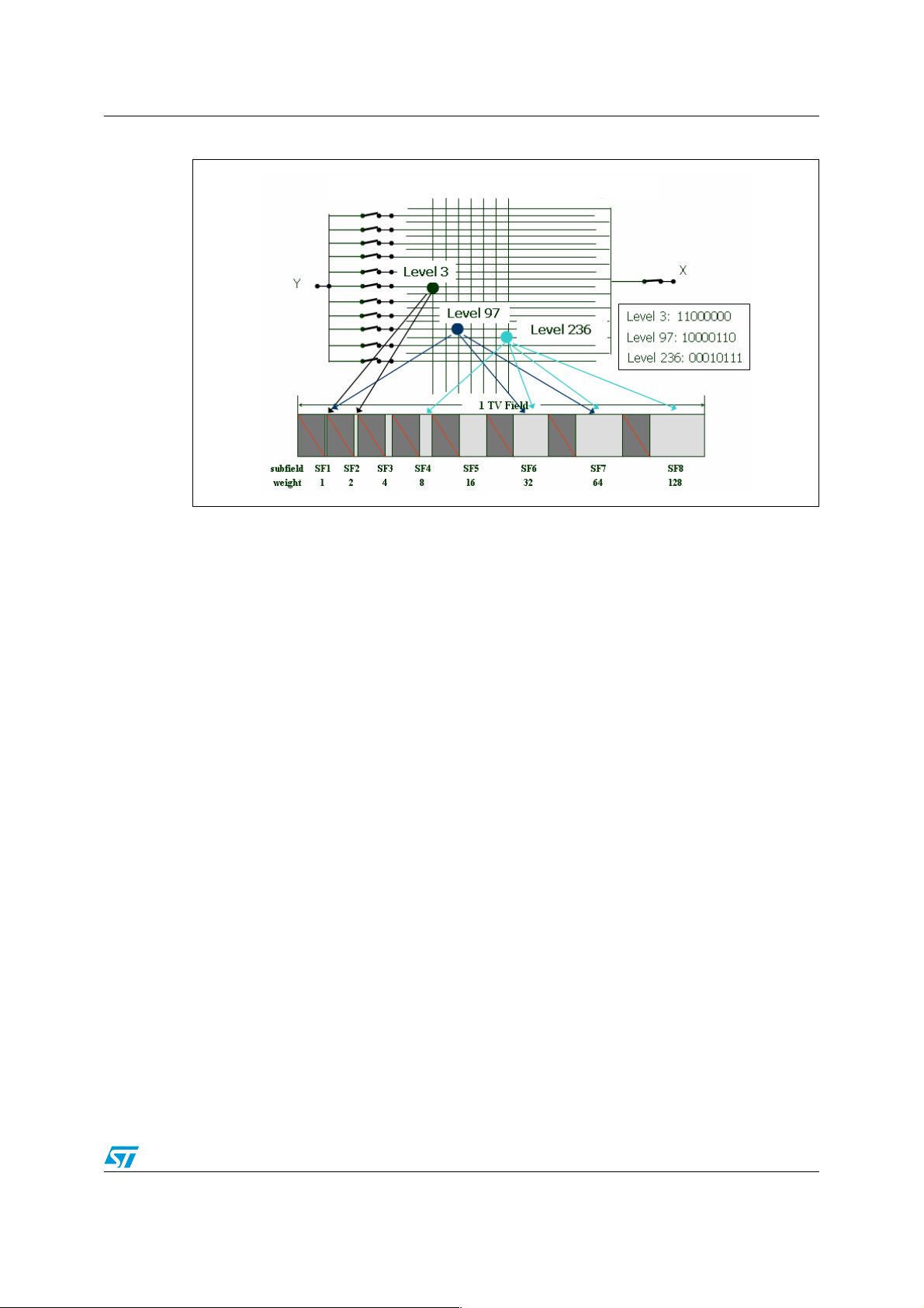
During sustain period, selected cells are sustained in order to display the whole image on
the panel. Gray scales are expressed by using the binary-coded light-emission-p e riod
method. The display periods are filled with trains of constant width and constant period
pulses, and their lengths are arranged according to the binary sequence, 1: 2: 4: 8: 16: 32:
64: 128: 256: 512. Therefore, gray levels of 2
expressed with an 10-bit sequence. This means that each color element has 1024 color
possible graduations and each pixel has 1024 x 1024 x 1024 = 1 billion colors. Figure 10
shows a simplified 8-bit system with 8 subfields. The subfields are weighted according to
their binary values and a typical TV field is 1/50 of a second.
10
for each color (R, G, and B) can be
8/30
Page 9
AN2503 PDP Sustain circuit
Figure 10. Subfield structure – expression of gray level
3 PDP Sustain circuit
In a Plasma Display Panel, frequent discharges are made to occur by alternately charging
each side of the panel to a critical voltage, allowing images to be displayed. This alternating
voltage is called the sustain voltage, and the sustain circuit (or sustainer) is needed to
provide it to the display [5.].
If a pixel has been driven "ON" during address period, the sustainer maintains the "ON"
state of that pixel by repeatedly discharging that pixel cell during the whole sustain period. If
a pixel has been driven "OFF" b y an a ddress driver, the voltage across the cell is nev er high
enough to cause a discharge, and the cell remains "OFF" during the sustain period.
The sustain circuit must drive all panel pixels at once. This means that the capacitance as
seen by the sustainer is typically v ery large. In a 42-inch panel with 852x480 pix e ls, th e total
capacitance of all the pixel cells, Cp, could be as much as 80 nF.
The key parameters in the sustainer study are:
● Cp - Panel equivalent capacitance
● Vs - Sustain Voltage
● f - Sustainer Switching frequency
● f
Conventional sustain circuit (half bridge topology) drives the panel directly, and thus
1/2C
ground.
- average sustainer switching frequency
av
2
f
PVS
is dissipated in the sustainer when the panel is subsequently discharged to
av
In a complete sustain cycle, each side of the panel is charged to Vs and subsequently
discharged to ground. Therefore, a total of 2CpVs
2
fav power is dissipated in a complete
sustain cycle.
9/30
Page 10

PDP Sustain circuit AN2503
Conventional sustain circuit (half bridge topology) drives the panel directly, and thus
1/2C
2
fav is dissipated in the sustainer when the panel is subsequently discharged to
PVS
ground.
In a complete sustain cycle, each side of the panel is charged to Vs and subsequently
discharged to ground. Therefore, a total of 2C
PVS
2
f
is dissipated in a complete sustain
av
cycle.
Figure 11. Sustain circuit
The power dissipation in the sustainer is th en 2C
2
fav, where fav is the average sustain
PVS
cycle frequency.
For Cp=80 nF, Vs =200 V, and f
= 100 kHz, the power dissipation in th e sustainer, resulting
av
from driving the capacitance of the panel, could be as high as 640 W.
If an inductor is placed in series with the panel, then Cp can be charged and discharged
through the inductor. This would ideally result in zero power dissipation since the inductor
would store all of the energy otherwise lost in the output resistance of the sustainer and
transfer it to or from Cp . Ho we v er , s wit ching de vices are neede d to control the flow of ene rg y
to and from the inductor, as Cp is charged and discharged, respectively, and this leads to
power losses.
The "ON" resistance, output capacitance, and switching transition time are characteristics of
these switching de vices that can result in significant energy loss. The amount of energy that
is actually lost due to these characteristics, and hence the efficiency, is determined largely
by how well the circuit is designed to minimize these losses. In addition to charging and
discharging Cp, the sustainer must also supply the large gas discharge current for the
plasma panel. This current, I, is proportional to the number of pixels that are "ON" in the
same TV frame. The resulting instan taneous power dissipation is I
resistance of the sustainer. Thus, the power dissipation due to the discharge current is
proportional to I
2
, or the square of the number of pixels that are simultaneously "ON".
2
R, where R is the output
There are two ways to minimize this dissipation. The first is to reduce the output resistance
of the sustainer by using very low resistance output drivers, and the second is to minimize
the number of pixels that are "ON" at any time.
The switching power losses due to the panel capacitance during sustain period in AC PDP
driving system can be minimized using a specific energy recovery circuit. The most common
sustain/energy recovery circuit topology refers to Weber topology (Figure 12).
10/30
Page 11
AN2503 PDP Sustain circuit
Figure 12. Circuit scheme
Vs Vs VsVset
L1
T3
T6 T5
T4
Y-Electrode
Cp
T9
X-Electrode
T10
D8
D5
T11
L7
T12
D7
D6
CS2
T7
T8
-Vreset
CS1
Vs
D2
T2
T1
D3
D1
D4
Weber topology provides a new sustainer circuit that recovers the energy otherwise lost in
charging and discharging the panel capacitance , Cp . The efficiency with which the sustainer
recovers this energy is defined as the "recovery" efficiency. In particular, when Cp is
charged to V
2
C
.
PVS
and then discharged to zero, the energy that flows into and out of Cp is E =
s
The recovery efficiency is defined by:
Equation 1
2
E
–
Eff 100
C
PVS
-----------------------------------------
CPV
LOST
2
S
⎛⎞
E
LOST
----------------- -–
•=•=
100 1
⎜⎟
⎝⎠
CPV
2
S
where E
is the energy lost in charging and discharging Cp in the sustain circuit without
LOST
energy recovery.
It is worth noting that the recovery efficiency is not the same as the conventional power
efficiency defined in terms of the power delivered to a load, since no power is delivered to
the capacitor Cp. It is simply charged and then discharged. The recovery efficiency is a
measure of the energy loss in the sustainer, and could reach a value higher than 90%.
Summarizing, the panel's pixels are connected in parallel and can be represented as an
equivalent panel capacitor Cp. A proper switching sequence, together with the energy
recovery circuit, allows this circuit to produce an AC voltage required to illuminate, recover
residual energy and reset the cells of the panel.
Referring to the schematic in Figure 12, Power de vices in the Sustain circuit top ology can be
grouped into four circuit sub-functions:
1. Energy recove ry circuit (ERC) which consists of T1, T2, T11, T12, D1, D2, D3, D4, D5,
D6, D7, D8
2. Sustain circuit (discharge circuit or sustainer) which consists of T3, T4, T9, T10
3. Path circuit which consists of T5, T6
4. Set and Reset circuit which consists of T7, T8
11/30
Page 12

PDP Sustain circuit AN2503
3.1 Sustain circuit operations
Sustain circuit operations describe the way to generate a square wa veform on the panel
capacitor. This section describes how t o charge and dischar ge the pa nel capacit or in or der
to perform the sustain phase.
3.1.1 Positive pulse of V
After the reset period, we can suppose that all cells on the panel have been already
addressed during the address period. This means that the cells to be displayed have
accumulated enough wall charge to be ignited, due to cell memory effect. We can assume
also that CS1 and CS2 have already their steady state voltage value, this means they have
initial voltage of V
In order to produce a positive voltage across the panel (V
are turned ON and D1 is forward biased. CS1 charges and raises the voltage across the
panel capacitor Cp in a resonant way. This step is a part of the energy recovery phase since
it recovers the energy stored in the capacitor CS1 from previous sustain cycles back to the
panel.
Figure 13. Circuit scheme – positive pulse of V
T2
CS1
T1
/2 from previous sustain cycles.
s
Vs
D2
D3
D1
D4
yx
L1
Vs Vs VsVset
T3
T6 T5
T4
positive), T1, T5, T6 and T10
yx
yx
T7
Y-Electrode
T8
T9
X-Electrode
Cp
L7
T10
D8
D5
T11
T12
D7
D6
CS2
The equivalent circuit during the LC resonant period of the energy recovery circuit is:
Figure 14. Equivalent circuit
In Figure 14, R represents the parasitic resistance including on-resistances of switches and
V
represents the diode forward drop. Based on this figure, the panel voltage V
ON
obtained as follows:
Equation 2
V
s
⎛⎞
V
12/30
------ V
yx
–
ON
⎝⎠
2
-Vreset
t
-- -–
τ
⎛⎞
1e
–=
⎝⎠
R
------
ωtcos
ωL
ωtsin+
can be
yx
Page 13

AN2503 PDP Sustain circuit
Where
If (2L/R)
ωR
⎛⎞
τ
=
⎝⎠
2
and (ωR/L) can be ignored, t he equation (Equation 2) can be simply re-written as:
-------
and
L
ω
1
⎛⎞
-----------
⎝⎠
LCp
R
⎛⎞
------ -
–=
⎝⎠
2L
2
Equation 3
t
---
τ
1e
ωcos–= t
Where
If ω’ =
ω
∏ then the peak value is:
1
-----------=
’
LCp
V
------ VON–
yx
⎝⎠
2
V
s
⎛⎞
Equation 4
C
πR
p
-------
V
s
V
yx pk,
⎛⎞
------ VON–
⎝⎠
2
1e
–=
------–
2
L
Equation 4 states that an increase of the parasitic resistance ca uses the reco very efficiency
to be degraded. Naturally, it is necessary to reduce the parasitic resistance by desig ning the
circuit board optimally as well as choosing s witching devices with small on-resistance and
low on-drop voltage to minimize the hard-switching stress and improve the recovery
performance. On the other hand, reduction of the inductor value produces similar results
and, thus, using a too small value of L is not desirable with respect to driving loss.
3.1.2 Positive discharge and clamping phase
Figure 15 shows both panel discharge and the camping current paths. In the f irst phase t he
ionized gas could be represented as a non linear resistor and the peak current during this
period is higher than that during energy recovery. The worst condition is represented when
all cells in the panel must be ignited (full white screen condition), and in this case the
discharge current could be higher th an 120 A f or a standa rd definition (SD) 4 2-inch PDP set.
Further increase in the current value is expected in HD PDP as the number of pixels
increases.
Figure 15. Circuit scheme – positive discharge and clamping
Vs Vs VsVset
L1
T3
T6 T5
T4
T7
-Vreset
CS1
Vs
D2
T2
T1
D3
D1
D4
Y-Electrode
Cp
T8
T9
X-Electrode
T10
D8
D5
L7
D7
T11
T12
D6
CS2
13/30
Page 14

PDP Sustain circuit AN2503
The discharge current has also a sinusoidal profile , and is conduct ed b y T3, T6, T5, Cp , and
T10. Once the panel is charged to Vs and visible light is emitted, current stops flowing and
the gas inside the glass stops ionizing. (Note that th e us e of I GBTs in the discharg e section
requires extra care; indeed power devices requires freewheeling diodes to carry reverse
current due to the tank circuit formed between the panel capacitor Cp, L1 and the bus
capacitance).
At this time D1 is reverse biased and its reverse cur rent charges the inductance L1. The
energy stored in the ind uctance is rem oved through the clamping current, and the clampin g
current path is carried out by T3, D3, and D2. In this phase the re v erse curren t of D1 is a ke y
parameter in power loss re duction. In f act, a lower clampi ng current means lower conduction
losses in T3, D2 and D3. Depending on the topology used, and in particular the clamping
diode's position, the time spent to evacuate the energy stored in the inductance can vary
significantly.
3.1.3 Vyx back to zero
The next phase consists of bringing back to zero the pane l capacitor v oltage and re v erse the
polarity of the voltage across Y-X electrodes.
In order to efficiently decrease the voltage on the panel capacitor, the energy stored in Cp
could be recovered bac k in the recovery capacitor CS1.This can be done by turning ON T2,
T6, T5, and T10.
The current path is shown in Figure 16. This current stops flowing when the voltage across
the panel capacitance V
is half sinusoidal and its direction is from the panel Cp back to CS1.
Figure 16. Circuit scheme – V
Vs
D2
D3
T2
CS1
T1
D1
D4
3.1.4 Clamping to ground
In order to bring completely to zero the panel capacitance, T10, T5, T6, and T4 are turned
ON, creating a current path across the panel through the equivalent resistances of power
devices and parasitic elements of the circuit.
and CS1 reach the same value (Vs/2). The profile of this current
yx
back to zero
yx
Vs Vs VsVset
T3
L1
T6 T5
T4
T7
Y-Electrode
T8
-Vreset
T9
X-Electrode
Cp
L7
T10
D8
D5
T11
T12
D7
D6
CS2
14/30
Page 15

AN2503 PDP Sustain circuit
Figure 17. Circuit scheme – clampin g to ground
Vs
Vs Vs VsVset
T3
T6 T5
T4
CS1
D2
D3
T2
T1
D1
D4
L1
3.2 Symmetrical Y - X phase
A similar switching sequence is applied in order to re ve rse the polarity across Y-X electrodes
(X electrode more positive than Y electrode)
In particular, this can be briefly described as:
a) Energy recovery, path and discharge switches, T12, T5, T6, and T4 are turned
ON, and the current flows from CS2 to Cp.
Figure 18. Circuit scheme – negative pulse of V
Vs Vs VsVset
L1
T3
T6 T5
T4
CS1
Vs
D2
T2
T1
D3
D1
D4
T7
Y-Electrode
T8
-Vreset
T9
X-Electrode
Cp
L7
T10
D8
D5
T11
T12
D7
D6
CS2
yx
Y-Electrode
Cp
T9
X-Electrode
T10
D8
D5
L7
D7
T11
T12
D6
CS2
T7
T8
-Vreset
b) Discharge and Clamp phases: T9, T4, T5, T6 are turned ON and the current flow s
from Vs to Cp and through T9, L7, D7, D8.
Figure 19. Circuit scheme – negative discharge and clamping
Vs Vs VsVset
L1
T3
T6 T5
T4
T7
Y-Electrode
T8
-Vreset
T9
D8
D5
X-Electrode
Cp
L7
T10
D7
D6
CS1
Vs
D2
D3
T2
T1
D1
D4
T11
T12
CS2
15/30
Page 16

PDP Sustain circuit AN2503
2
c) Energy Recovery phase: T4, T5, T6, and T11 are tu rned ON, and the current flo ws
from Cp to CS2.
Figure 20. Circuit scheme – V
Vs
D2
D3
T2
S1
T1
D1
D4
L1
back to zero
yx
Vs Vs VsVset
T3
T6 T5
T4
T7
-Vreset
d) Zero voltage Clamp, T4, T5, T6, T10 are turned ON.
Figure 21. Circuit scheme – clampin g to ground
V
D
T T T
CS
D
D
V V VVse
L
T
T
Y
E
l
e
c
Y-Electrode
Cp
T8
C
T
T9
X-Electrode
L7
T10
T
X-Electrode
L
T1
D8
D5
T11
T12
D7
D6
D
D
D
T1
T1
D
CS
CS
It can be noted that during sustain phase, path switches T5 and T6 are always turned ON,
and they see both energy recovery current and discharge current which explains the need
for low voltage drop devices.
3.3 Reset phase
At the end of each subfield, the cells are reset a pplying a positive ramp v oltage f ollow ed by a
negative one.
During positive reset, T10, T5, T7 are turned ON. During negative reset T10 and T8 are
turned ON.
16/30
Page 17

AN2503 PDP Power Devices characteristics
Figure 22. Circuit scheme – set and reset
Vs Vs VsVset
L1
T3
T6 T5
T4
T7
X-Electrod e
Y-Electrod e
Cp
T8
-Vreset
CS1
Vs
D2
T2
T1
D3
D1
D4
4 PDP Power Devices characteristics
A clear idea of circuit operation will help us to highlight the main features of the devices
involv ed. In particular the analysis can be split in power de vices analysis and driving devices
analysis, in order to address specific characteristics of each device.
4.1 Power devices from ST
T9
L7
T10
D8
D5
D7
T11
T12
D6
CS2
Power devices in PDP have common characteristics that range from high peak current
capability and low forward voltage drop to fast turn-ON capability. The current both in the
Energy Recovery Circuit (ERC) and in the Discharge Circuit (DC) follows a half sinusoidal
pattern. ERC and DC could be simply classified as soft switching converters. In fact, the
circuit can be considered as a series resonant LCR circuit, so the current at turn-ON is zero
(zero current switching) and the voltage at turn-OFF is zero (zero voltage switching).
Since a MOSFET has an intrinsic body diode across it, a MOSFET does not require an antiparallel diode when selected as power devices on the discharge circuit, while an IGBT
needs a specific freewheeling diode. For ER circuit, the Power Switch does not require an
anti-parallel diode since re verse current is blocked by the diodes in series with the devices
(D1, D3, D5 and D7), thus MOSFET or IGBT can be used as power devices on the ER
circuit.
Diodes D2, D4, D6 and D8 provide additional pr otection clamping the voltage on the
inductors avoiding damage to devices on the ER circuit.
Path circuit has to carry both ER and Discharge currents , thus it is required to hav e v ery low
voltage drop. It can be noted that during ER and Discharge cycles, the pass circuit remains
on. The Path circ uit switches on and off only during reset period which happens at the end
of each subfield, which means that the maximum frequency is in the range of 1 kHz. The
Path circuit is a bidirectional circuit, so a MO SFET, that can carry current in both directions,
could be used for this circuit.
ST has a broad range of products covering the power section ranging from MOSFET and
IGBT to dedicated Diodes.
17/30
Page 18

PDP Power Devices characteristics AN2503
4.1.1 Measurement set-up
Po wer losses and thermal analysis measurements were performed based on an average
switching frequency. In fact, switching performances have to be related to the maximum
frequency in the system, usually 250 kHz, whereas power losses a nd thermal management
have to be related to an average frequency. The Average Switching frequency takes into
account the fact that during a picture time , the po w e r devices do not switch at the maximum
frequency for the whole time, but only during the sustain phases. The sust ain duration, and
consequently the number of sustain pulses , increases starting from subfield 1 to su bfield 10.
Average frequency can be calculated starting from sustain duty ratio.
Table 1. 10 subfield / single scan
Scan speed VGA 480 XGA 768 HD 1080
3 µsec - - -
2.5 µsec 0.130 - 2 µsec 0.274 - -
1.5 µsec 0.418 0.159 1 µsec 0.562 0.389 0.202
Table 2. 10 subfield / dual scan
Scan speed VGA 480 XGA 768 HD 1080
3 µsec 0.418 0.158 -
2.5 µsec 0.490 0.274 0.040
2 µsec 0.562 0.389 0.202
1.5 µsec 0.634 0.504 0.364
1 µsec 0.706 0.620 0.526
Note: Sustain duty = picture time - reset period x SF - N x SF x scan speed [
Picture time = 16.67 ms
Reset period = 250
µsec
SF = number of sustain pulses
N = number of lines
The sustain duty ratio is carried out for a 10 subfield case in b oth single scan and dual scan
operations, varying the scan speed duration (time needed to scan a single line in the
display), for VGA (480 lines), XGA (768 lines) and HD (1080 lines).
According to the following formula,
f
av=fswitching
For a VGA display
x SustainDuty
→ SustainDuty = 0.27 ÷ 0.56 → f
= 68 ÷ 140 kHz
av
This means that power devices in ERC and discharge circuit need to be designed for an
average frequency of 140 kHz (maximum) in terms of power losses and thermal
management. Clearly peak current and peak v o ltage r ating do not chang e when w e perf o rm
this averaged analysis.
µs / line]
18/30
Page 19

AN2503 PDP Power Devices characteristics
Typical voltage requirements for a PDP are:
● Sustain voltage Vs = 200 V
● Set voltage Vset= 400 V
● Reset voltage Vreset= -150 V
4.1.2 Energy recovery section
For Energy recovery circuit, the maximum voltage stress is Vs/2 ≈ 100 V, and the current
stress depends on the device. The clamping diodes have to withstand a current lower than
10 A, whilst the ERC switches and the ERC diodes have to be able to handle a resonant
half-sinusoidal current up to 100 A peak.
The typical current waveform in the Energy recovery circuit is shown in Figure 23. The key
parameters of the DERC diode for the energy reco very circuit have been optimized in order
to decrease power losses.
Figure 23. Inductor current
ERC
current
T1
Clamping
current
T3
D2
D3
For ER circuit new devices with low voltage drop and very fast turn ON hav e been
developed.
● Energy recovery diodes STTH60P03, STTH40P03
Energy recovery diodes (D1, D3, D5, and D7) have been tailored on this application
optimizing key parameters to reduce power losses [6.], [7.]. They have the ability to handle
large repetitive peak current ( Irp), in conjunction with a lower r e v erse current (I
forward voltage (V
FP
).
) and peak
RM
Table 3. STTH60P03 Features
Symbol Parameter Test conditions Min. Typ Max. Unit
I
S
V
RM
factor
FP
Reverse
recovery current
T
= 100°C
j
Softness factor 0.5
Peak forward
voltage
= 25°C
T
j
= 60 A VR =
I
F
100 V
/dt = 200 A/µs
dI
F
I
= 60 A
F
dIF/dt = 400 A/µs
67.5A
2.5 3.5 V
19/30
Page 20

PDP Power Devices characteristics AN2503
● Clamping diodes STTH2003, STTH1003
Diodes D2, D4, D6, and D8 provide additiona l protection to clamp the voltage on the
inductors [8], [9]. Overvoltage is due to ER diodes reverse current that store energy in the
inductors. The fa ct that reverse current I
of ERC diodes stores energy in the inductors
RM
(and can cause ov ervoltage if we do not use clamping diodes D2, D4, D6, and D8),
demonstrates that the I
I
causes power losses both in Clamping diodes and Discharge switches.
RM
in ERC diodes is a key parameter to take into account. In fact,
RM
Table 4. Clamping diodes features
P/N IF [A] V
STTH1003 10 300 13 175 0.9 DPAK, TO-220FP, D
STTH2003 2x10 300 35 175 1 DPAK, TO-220FP, D
● Energy recovery MOSFET ST75N20
T1, T2, T11, and T12 are the power switches used in the Energy recovery circuit. Due to the
reactive nature of the load, th e voltage across the power switch falls rapidly followed by a
rapid rise in the current. This explains why a fast turn-ON is needed, and low conduction
losses (low drop) can be achieved only reducing the R
MOSFET in proprietary STripFET
charge is perfectly tailored for the application [9.].
Table 5. ERC MOSFET features
P/N V
ST75N20 200 0.028 75/300 300 TO-247, TO-220, D
DSS
[V] R
4.1.3 Discharge section
When the panel discharges, a sinusoidal shaped current will go through the discharge
switches. The curre nt could reach a peak value higher than 120 A in worst condition (full
white screen), thus low R
Maximum voltage stress for discharge circuit is Vs = 200 V
● Discharge MOSFET STW52NK25Z
The STW52NK25Z Power MOSFET in property superMESH
low R
and low gate charge is perfectly tailored on the application [10.].
DSON
[V] Trr [ns] Tj[C] VF[V] Package
RRM
. The STW75N20 Power
TM
technology, thanks to its low R
[Ω] ID/I
DSON
and fast turn-ON are required.
DSON
[A] P [W] Package
DMAX
DSON
DSON
TM
technology, and due to its
2
PAK
2
PAK, TO220
and low gate
2
PAK
Table 6. Sustain MOSFET features
P/N V
STW52NK25Z 250 0.033 52/208 300 TO-247 STW52NK25Z
STW54NK30Z 300 0.060 54/200 300 TO-247 STW54NK30Z
DSS
[V] R
DSON
[Ω] ID/I
4.1.4 Path section
For Path circuit, MOSFET is the preferred device since this circuit is required to conduct
current in both directions. The switching frequency is low, and the RMS current through this
20/30
[A] P [W] Package P/N
DMAX
Page 21

AN2503 PDP Power Devices characteristics
circuit is very large since it has to conduct both ER and discharge currents. Both
STripFET
TM
and superMESHTM Power MOSFETs technologies from ST are ideal for this
application since they allow the die to have very high current density and therefore reduce
the number of paralleled devices required to maintain very low voltage drop [9.], [10.], [11.],
[12.].
For path s witch in T6 position, the maximu m v oltage st ress is (Vs + Vset) / 2 ≈
for path switch in T5 position, the maximum voltage stress is (Vset + |Vreset|) / 2 ≈ 275 V.
Table 7. Path MOSFET features
P/N V
ST60NK30ZD1 300 0.045 60/240 450 Die or MAX247
STW52NK25Z 250 0.033 52/208 300 TO-247
ST75N20 200 0.028 75/300 300 TO-247, TO-220, D
ST40N20 200 0.045 40/160 160
DSS
4.1.5 Set - reset section
The set and reset circuit applies asymmetrical AC voltage across the panel in order to
evacuate any remaining surface charge from the cells. This is usually done at the end of
each subfield (or the beginning of the next subfield), and the power devices on this circuit
operate in the linear mode. This mea ns that the voltage drop is very large but the current
through the device is relatively low. Due to the requirement of asymmetrical Set and Reset
voltages, Power switches in the set and reset circuits have to block up to 600 V. Typical
voltage value for Set function is 400 V and for Reset function is -150 V. This means that the
maximum voltage stress for Set circuit T9 is (Vs + Vset) = 600 V while the maximum voltage
stress for reset circuit T10 is Vset + |Vreset| = 550 V.
[V] R
DSON
[Ω] ID/I
[A] P [W] Package
DMAX
TO-247 TO-220 D
300 V, while
TO220FP
2
PAK
2
PAK
ST offers two families of products for this section both appreciable for their ruggedness for
linear applications.
Example device is STGP10NB60S in the IGBT Planar technology [13.]:
Table 8. Set – reset IGBT features
P/N V
STGP10NB60S 600 1.7 10 D
[V] V
CES
[Ω] IC [A] Package
CE(SAT)
2
PAK
Further examples of devices are superMESHTM devices as follows [14.], [15.].
Table 9. Set-reset MOSFET features
P/N V
ST9NK70Z 700 1 7.5/30 115 W TO-220 D
ST14NK60Z 600 0.5 13.5/54 160 W TO-220 D
DSS
[V] R
DSON
[Ω] ID/I
[A] P [W] Package
DMAX
2
PAK TO220FP
2
PAK TO220FP
21/30
Page 22

PDP Power Devices characteristics AN2503
4.2 Driving section
Driving section devices range from gate driver devices to input buffer ones. Gate driver
function is carried out by a gate driver IC and a push pull amplifier.
Driving section can be split in:
● Gate driver section: L6385 or L6388
● Push pull section: STS01DTP06
● Input buffer section 74VHCT541
4.3 Gate driver devices
ST offers the widest series among the High Voltage Half-Bridge Gate Drivers (the L638x
series), manufactured with BCD"OFF-LINE" technology. They are able to work in
applications with with voltages to 600 V. In the L638x series the two selected drivers are the
L6388 [16.] and the L6385 [17.], which can drive two Power MOSFETs or IGBTs, one highside and one low-side, in a Half-Bridge or different topology. L6388 is especially effective in
applications where logic input must be compatible with 3.3 V Logic. Another key feat ure of
the L6388 is that it provides effective anti-shoot-through circuitry which prevents two Power
MOSFETs or IGBTs from being turned ON at the same time. This is achie v ed by introd ucing
a 200 ns time interval, a "dead time" between the moment one of the components is turned
OFF and the other is turned ON. L6385 is able to drive asymmetrical half bridge, but its
logic input is not compatible with 3.3V Logic.
The main features of these HV Gate Drivers are:
● dV/dt immunity +- 50 V/nsec in full temperature range
● Driver current capability:
– 400 mA source
– 650 mA sink
● Switching time 50/30 nsec rise/fall with 1 nF load
● Under voltage lock-out on lower and upper driving section
● Internal bootstrap diode
● Outputs in phase with inputs
Due to different char acteristics, the to pologies used in Ene rgy Recovery Circuit and Sustain
Circuit depend on the driver used as shown in Figure 24 and Figure 25.
22/30
Page 23

AN2503 PDP Power Devices characteristics
Vcc
HIN
LIN
GND
1
3
2
4
OUT
HVG
Vboot
8
7
6
5
LVG
VCC
L638x
VCC
TO PLASMA
Vs
Vs
Vs
Vs
Vcc
HIN
LIN
GND
1
3
2
4
OUT
HVG
Vboot
8
7
6
5
LVG
VCC
L638x
VCC
Vs/2
Vs/2
PP
PP
PP
PP
pgy
Vs
Figure 24. Gate driver topology with L6385
Figure 25. Gate driver topology – L6388
Vs
Vs
L638x
GND
8
Vboot
LIN
HVG
HIN
OUT
Vcc
LVG
PP
7
6
5
VCC
Vs/2
TO PLASMA
PP
VCC
1
2
3
4
L638x
GND
8
Vboot
LIN
HVG
HIN
OUT
Vcc
LVG
PP
7
6
5
VCC
VCC
1
2
3
4
PP
Due to current value in bootstrap charge, the internal diode cannot be used, thus external
diode SMBY01-400 [20.] must be used. Further details on L6585 and L6588 application can
be found in [18.] and [19.].
4.3.1 Totem pole
In order to match inherent power devices characteristics, (as high gate charge) with drivers
current capability, totem pole STS01DTP06 [21.] in a push pull configuration is used in the
application. The STS01DTP06 is housed in the SMD dual island SO-8 package and allows
an optimized electronic solutions, b y impro ving circuit efficie ncy, saving space and reducing
component count on the board.
The STS01DTP06 is a hybrid complementary NPN and PNP bipolar transistor
manufactured using the latest low voltage planar technology. Extremely efficient
performance is obtained by combining high pulse cur rent, excellent gain and fast speed,
23/30
Page 24

PDP Power Devices characteristics AN2503
resulting in low losses in high frequency applications. The STS01DTP06 offers a 30 V NPN
and PNP combination supporting a continuous collector current of 3 A and the minimum
gain of the two transistors is 100 at 1 A collector current. The transistor elements are fully
independent so that higher assembly flexibility is guaranteed. Concerning PDPs, this means
that the turn-ON and the tu rn-OFF resistors could be different.
Figure 26. STS01DTP06 Totem pole
The STS01DTP06 main features are summarized in Table 10:
Table 10. STS01DTP06 Features
Part number
[V] Ic[A] P
V
NPN PNP
STS01DTP06 30 3 1.6 100 0.7 2 100
CEO
4.4 Input buffer section
The 74VHCT541 is an advanced high-speed CMOS OCTAL BUS BUFFER (3-STATE)
fabricated with sub-micron silicon gate and double-layer metal wiring C2MOS technology,
available in TSSOP package [22.].
In order to enhance PC board layout, the 74VHCT541 offers a pin-out having inputs and
outputs on opposite sides of the package. The device is characterized by high speed and
low power dissipation. Power down protection is provided on all inputs and 0 to 7 V can be
accepted on inputs with no regard to the supply voltage. This device can be used to
interface 5 V to 3 V. All inputs and outputs are equipped with protection circuits against static
discharge, giving them 2KV ESD immunity and t ransient excess voltage.
[W] hFEmin VCE(sat)@ MAX [V] Ic[A] IB[mA]
tot
24/30
Page 25

AN2503 Bill of material and schematics
5 Bill of material and schematics
Table 11 gives the BOM and the schematics of the demo board.
Table 11. Bill of material
Item Qty Reference Value & comment
1 5 C1,C4,C23,C26, C44 2.2 µF 50 V
2 5 C2,C3,C24,C25,C45 100 nF 50 V
3 4 C5,C6, C20,C21 2.2 nF 400 V
4 4 C16,C17,C18,C19 3.3 µF 250 V
5 1 C22 104 K 250 V
6 8 C27,C28,C29,C30,C48,C49,C50,C51 100 µF 250 V
7 2 C35,C36 100 µF 25 V
8 7 C37,C38,C39,C40,C41,C42,C43 100 pF 10 V
9 2 C46,C47 X1 Capacitor modeling the panel
10 4 D1,D7 SMBY01-400
11 2 D2,D10 STTH60P03SW
12 3 D3,D8 STTH2003CG
13 3 D14 DIODE Z.16 V
14 1 F1 5A 250 V Fuse
15 2 F2,F3 1A 125 V
16 1 J1 HEADER 9
17 2 J4,J13 Connector 2 PINS
18 1 J7 GND-STAR Connector
19 1 J18 HEADER 30
20 2 L5,L6 500 nH inductor
21 2 L12,L14 10 µH inductor
22 2 R2,R19 2,2 Ω SMD resistor
23 8 R7,R8,R9,R10,R17,R18,R21,R22 3.9 Ω SMD resistor
24 2 R1, R20 36 Ω SMD resistor
25 5 R35,R36,R37,R38,R39 200 Ω SMD resistor
26 4 R50, R51 100 KΩ SMD resistor
27 6 R3, R4, R23, R24, R25 1 Ω SMD resistor
28 6 R26,R40,R41,R42,R43,R44 100 Ω SMD resistor
29 3 R27 10 KΩ SMD resistor
30 2 U1,U5 L 6385
31 4 U2,U3,U6,U7 STS01DTP06
25/30
Page 26
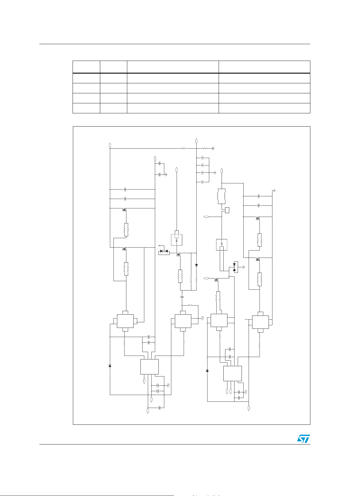
Bill of material and schematics AN2503
V sustainV sustain
VCC
C26
22uF-50V
U16
STW52NK25Z
U6
STS01DTP06
12
34
5
6
7
8
E1B1
E2B2
C2
C2
C1
C1
C25
100nF
C47
X1
C21
2.2nF
C19
3.3uF 250v
C16
3.3uF 250v
R27
10K
D14
DIODE Z.16v
R17
3.9
R51
100K
U7
STS01DTP06
12
34
5
6
7
8
E1B1
E2B2
C2
C2
C1
C1
U5
L 6385
123
4 5
678
LIN
HIN
VCC
GND LGV
VOUT
HGV
Vboot
U15
STW75N20
C23
22uF-50V
C17
3.3uF 250v
C31
33pF
R19
2.2
D10 STTH60P03SW
A1KA2
R20
36
R24
1
C22
104K 250V
C18
3.3uF 250v
R21
3.9
C24
100nF
R26100
U14
STW52NK25Z
D8
STTH2003CG
R50
100K
C20
2.2nF
R251K
R231
R22
3.9
D7
SMBYT01-400
C46
X1
R18 3.9
U11
STW52NK52Z
R7 3.9
R4 1
R3 1.
U13
STW75N20
C4
22uF-50V
D1
SMBYT01-400
R9
3.9
C3
100nF
R2
2.2
R8 3.9
C6
2.2nF 400v
J4
CON2
1
2
D2
STTH60P03SW
123
A1KA2
C2
100nF
C1
22uF-50V
U3
STS01DTP06
12
34
5
6
7
8
E1B1
E2B2
C2
C2
C1
C1
D3
STTH2003CG
U2
STS01DTP06
12
34
5
6
7
8
E1B1
E2B2
C2
C2
C1
C1
L6 500nH
C5
2.2nF 400v
R10
3.9
U12
STW52NK25Z
L5 500nH
U1
L 6385
123
4 5
678
LIN
HIN
VCC
GND LGV
VOUT
HGV
Vboot
R1
36
LIN U4005
V sustain/2
V sustain
HIN U4005
Display
VCC
Res IND
VCC
Display
Res INDV sustain/2
HIN U4004
LIN-U4004
T11
T10T10
T12
T9 T9
Table 11. Bill of material (continued)
Item Qty Reference Value & comment
32 1 U8 74VHCT541
33 4 U11,U12,U14, U16 STW52NK25Z
34 2 U13,U15 STW75N20
35 3 J15, J16, J17 Connector 17 pins
Figure 27. Board schematic 1
26/30
Page 27

AN2503 Bill of material and schematics
Figure 28. Board schematic 2
J15
123456789
F3
FUSErid
C42
100pF
C36
100uF 25v
VCCVDD
10111213141516
V sust ain
CONN SOCKET 17
J16
123456789
17
C51
C50
C49
C48
10111213141516
Display
Xs
LIN U4005
R44
100
R39
200
Xr
CONN SOCKET 17
J17
17
Xg
LIN-U4004
R40
100
R37
VDD
123456789
Xr
HIN U 4004
R41
100
200
Xf
R36
C44
22uF25v
C45
100nF
U8
1
2
J13
ENABLE
Xs
R42
200
19
20
18
19
20
18
123456789
123456789
XrXbXf
Xs
Xg
10111213141516
Xb
HIN U 4008
100
R35
200
11121413151617
10
Xg
CONN SOCKET 17
17
Xf
HIN U 4005
R43
100
R38
200
11121413151617
st74v hct 541
10
Xb
C43
100pF
C37
100pF
C38
100pF
C39
100pF
C40
100pF
C41
C35
100uF 25v
L12
10uH
F2
FUSErid
Vb
123456789
J1
C28 C29 C30
C27
R30
1K
R31
1K
R32
1K
R33
1K
100uF250V
L14
INDUCTOR
F1
FUSErid
1234567891011121314151617181920212223242526272829
HEADER 9
1
2
J7
GND-STAR
J18
100pF
R34
1K
30
HEADER 3 0
27/30
Page 28

Conclusions AN2503
6 Conclusions
ST offers its customers a complete product portfolio covering the whole PDP. ST's system
approach helps customers design effective energy recover (ERC) and Sustain circuits,
improving their time-to-market. PDP power consumption is greatly reduced using ST's
dedicated products.
7 References
1. "Plasma displays," IEEE Trans. Plasma Sci., vol. 19, pp. 1032-1047, Dec. 1991.
2. "Cell structure and driving method of a 25-in (64 cm) diagonal high-resolution color ac
plasma display," in Proc. Symp. Society for Information Display, vol. 29, 1998, pp. 279-
282.
3. "Charge spreading and its effect on AC plasma panel operating margins," IEEE Trans.
Electron Devices , vol. ED-24, pp. 870-872, July 1997.
4. "Measurement of wall charges in a surface discharge AC-PDP," in Proc. Int. Display
Workshops, 1997 , pp. 527-530.
5. " Power efficient sustain drivers and address drivers for plasma panel," U.S. Patent 4
866 349, Sept. 1989 and U.S. Patent 5 081 400, Jan. 1992.
6. STTH60P03SW Datasheet
7. STTH40P03SW Datasheet
8. STTH2003CG Datasheet
9. STW75N20 Datasheet
10. STW52NK25Z Datasheet
11. STP40N20 Datasheet
12. ST60NK30ZD1 Datasheet
13. STGP10NB60S Datasheet
14. STP9NK70Z Datasheet
15. STB14NK60Z Datasheet
16. L 6388 Datasheet
17. L 6385 Datasheet
18. AN994 - L6384, L6385, L6386, L6387 Application guide
19. AN1299 - L6384, L6385, L6386, L6387: TIPS & TRICKS
20. SMBY01-400 Datasheet
21. STS01DTP06 Datasheet
22. 74VHCT541 Datasheet
28/30
Page 29

AN2503 Revision history
8 Revision history
Table 12. Revision history
Date Revision Changes
02-May-2007 1 First issue
29/30
Page 30

AN2503
Please Read Carefully:
Information in this document is provided solely in connection with ST products. STMicroelectronics NV and its subsidiaries (“ST”) reserve the
right to make changes, corrections, modifications or improvements, to this document, and the products and services described herein at any
time, without notice.
All ST products are sold pursuant to ST’s terms and conditions of sal e.
Purchasers are solely res ponsibl e fo r the c hoic e, se lecti on an d use o f the S T prod ucts and s ervi ces d escr ibed he rein , and ST as sumes no
liability whatsoever relati ng to the choice, selection or use of the ST products and services described herein.
No license, express or implied, by estoppel or otherwise, to any intellectual property rights is granted under this document. If any part of this
document refers to any third pa rty p ro duc ts or se rv ices it sh all n ot be deem ed a lice ns e gr ant by ST fo r t he use of su ch thi r d party products
or services, or any intellectua l property c ontained the rein or consi dered as a warr anty coverin g the use in any manner whats oever of suc h
third party products or servi ces or any intellectual property contained therein.
UNLESS OTHERWISE SET FORTH IN ST’S TERMS AND CONDITIONS OF SALE ST DISCLAIMS ANY EXPRESS OR IMPLIED
WARRANTY WITH RESPECT TO THE USE AND/OR SALE OF ST PRODUCTS INCLUDING WITHOUT LIMITATION IMPLIED
WARRANTIES OF MERCHANTABILITY, FITNESS FOR A PARTICUL AR PURPOS E (AND THEIR EQUIVALE NTS UNDER THE LAWS
OF ANY JURISDICTION), OR INFRINGEMENT OF ANY PATENT, COPYRIGHT OR OTHER INTELLECTUAL PROPERTY RIGHT.
UNLESS EXPRESSLY APPROVED IN WRITING BY AN AUTHORIZED ST REPRESENTATIVE, ST PRODUCTS ARE NOT
RECOMMENDED, AUTHORIZED OR WARRANTED FOR USE IN MILITARY, AIR CRAFT, SPACE, LIFE SAVING, OR LIFE SUSTAINING
APPLICATIONS, NOR IN PRODUCTS OR SYSTEMS WHERE FAILURE OR MALFUNCTION MAY RESULT IN PERSONAL INJ URY,
DEATH, OR SEVERE PROPERTY OR ENVIRONMENTAL DAMAGE. ST PRODUCTS WHICH ARE NOT SPECIFIED AS "AUTOMOTIVE
GRADE" MAY ONLY BE USED IN AUTOMOTIVE APPLICATIONS AT USER’S OWN RISK.
Resale of ST products with provisions different from the statements and/or technical features set forth in this document shall immediately void
any warranty granted by ST fo r the ST pro duct or serv ice describe d herein and shall not cr eate or exten d in any manne r whatsoever , any
liability of ST.
ST and the ST logo are trademarks or registered trademarks of ST in various countries.
Information in this document su persedes and replaces all info rmation previously supplied.
The ST logo is a registered trademark of STMicroelectronics. All other names are the property of their respective owners.
© 2007 STMicroelectronics - All rights reserved
STMicroelectronics group of compan ie s
Australia - Belgium - Brazil - Canada - China - Czech Republic - Finland - France - Germany - Hong Kong - India - Israel - Italy - Japan -
Malaysia - Malta - Morocco - Singapore - Spain - Sweden - Switzerland - United Kingdom - United States of America
www.st.com
30/30
 Loading...