

Page 1

AN2487
Application note
STEVAL-TSP001V1
power over Ethernet powered device demonstration board
Introduction
This application note describes the STEVAL-TSP001V1 demonstration board for the
evaluation of a power over Ethernet (PoE) system used to transmit electrical power, along
with data, to remote devices over a standard twisted-pair cable in an Ethernet network.
A complete power solution for Ethernet-connected powered devices is presented. The
power supply fully complies with IEEE 802.3-2005 PoE specifications and delivers the rated
output from any compliant source.
Example outputs of 3.3 V and 12 V are given in this document, but other requirements can
easily be met by implementing small changes.
Key features
■ Low profile, small size: 5"w x 1.5"d x 0.65"h (0.5" except RJ-45 Ethernet connectors)
■ Complies with all IEEE 802.3-2005 (IEEE 802.3af) Power over Ethernet specifications
■ Respects source limitations
■ Does not pollute power source
■ 1500 V isolated outputs eliminate ground loops
■ Highest possible economical output power (total power at output approximately 10 W)
■ Useful output voltages
– 12 V @0.65 A output (7.8 W, loose tolerance)
– 3.3 V @0.65 A output (2.145 W, tight tolerance)
■ Increased cost-effectiveness due to SMT construction (through-hole connectors for
ruggedness)
August 2008 Rev 2 1/32
www.st.com
Page 2

Contents AN2487
Contents
1 Overview . . . . . . . . . . . . . . . . . . . . . . . . . . . . . . . . . . . . . . . . . . . . . . . . . . 5
1.1 Limitations on available power . . . . . . . . . . . . . . . . . . . . . . . . . . . . . . . . . . 5
2 Powered device demonstration board . . . . . . . . . . . . . . . . . . . . . . . . . . 6
2.1 Design choices . . . . . . . . . . . . . . . . . . . . . . . . . . . . . . . . . . . . . . . . . . . . . . 6
3 Circuit descriptions . . . . . . . . . . . . . . . . . . . . . . . . . . . . . . . . . . . . . . . . . 10
3.1 Inputs . . . . . . . . . . . . . . . . . . . . . . . . . . . . . . . . . . . . . . . . . . . . . . . . . . . . 10
3.1.1 Power supplies . . . . . . . . . . . . . . . . . . . . . . . . . . . . . . . . . . . . . . . . . . . . 10
3.1.2 Transient protection . . . . . . . . . . . . . . . . . . . . . . . . . . . . . . . . . . . . . . . . 11
3.1.3 Input capacitor . . . . . . . . . . . . . . . . . . . . . . . . . . . . . . . . . . . . . . . . . . . . 11
3.2 STHS4257 powered device interface controller . . . . . . . . . . . . . . . . . . . . 11
3.2.1 Sequence of operation . . . . . . . . . . . . . . . . . . . . . . . . . . . . . . . . . . . . . . 11
3.2.2 POE Signature resistance . . . . . . . . . . . . . . . . . . . . . . . . . . . . . . . . . . . 11
3.2.3 Classification . . . . . . . . . . . . . . . . . . . . . . . . . . . . . . . . . . . . . . . . . . . . . 11
3.2.4 Startup sequence . . . . . . . . . . . . . . . . . . . . . . . . . . . . . . . . . . . . . . . . . 12
3.2.5 Maintain power signature (MPS) . . . . . . . . . . . . . . . . . . . . . . . . . . . . . . 12
3.3 Power converter operation . . . . . . . . . . . . . . . . . . . . . . . . . . . . . . . . . . . . 13
3.3.1 Input filtering . . . . . . . . . . . . . . . . . . . . . . . . . . . . . . . . . . . . . . . . . . . . . 13
3.3.2 Startup . . . . . . . . . . . . . . . . . . . . . . . . . . . . . . . . . . . . . . . . . . . . . . . . . . 13
3.3.3 Regulation . . . . . . . . . . . . . . . . . . . . . . . . . . . . . . . . . . . . . . . . . . . . . . . 13
3.3.4 Critical conduction operation . . . . . . . . . . . . . . . . . . . . . . . . . . . . . . . . . 15
3.3.5 Outputs . . . . . . . . . . . . . . . . . . . . . . . . . . . . . . . . . . . . . . . . . . . . . . . . . 15
3.3.6 Miscellaneous component functions . . . . . . . . . . . . . . . . . . . . . . . . . . . 15
3.4 Transformer details . . . . . . . . . . . . . . . . . . . . . . . . . . . . . . . . . . . . . . . . . . 16
4 Electrical characteristics . . . . . . . . . . . . . . . . . . . . . . . . . . . . . . . . . . . . 17
4.1 Test setup . . . . . . . . . . . . . . . . . . . . . . . . . . . . . . . . . . . . . . . . . . . . . . . . . 17
4.2 STHS4257 powered device interface controller . . . . . . . . . . . . . . . . . . . . 17
4.2.1 Signature current . . . . . . . . . . . . . . . . . . . . . . . . . . . . . . . . . . . . . . . . . . 17
4.2.2 Classification current . . . . . . . . . . . . . . . . . . . . . . . . . . . . . . . . . . . . . . . 18
4.2.3 Undervoltage lockout . . . . . . . . . . . . . . . . . . . . . . . . . . . . . . . . . . . . . . . 18
4.3 Powered device supply solution . . . . . . . . . . . . . . . . . . . . . . . . . . . . . . . . 19
4.3.1 Current draw at low input voltage . . . . . . . . . . . . . . . . . . . . . . . . . . . . . 19
2/32
Page 3

AN2487 Contents
4.3.2 Power Good signal and capacitor charging current . . . . . . . . . . . . . . . . 19
4.3.3 Discussion . . . . . . . . . . . . . . . . . . . . . . . . . . . . . . . . . . . . . . . . . . . . . . . 19
4.4 Startup loading on the Power Sourcing Equipment . . . . . . . . . . . . . . . . . 19
4.4.1 Maintain power signature . . . . . . . . . . . . . . . . . . . . . . . . . . . . . . . . . . . . 20
4.5 STHS4257A1 voltage drop under load . . . . . . . . . . . . . . . . . . . . . . . . . . . 21
4.6 Input current limit vs input voltage . . . . . . . . . . . . . . . . . . . . . . . . . . . . . . 21
4.7 Characteristics of entire system . . . . . . . . . . . . . . . . . . . . . . . . . . . . . . . . 22
4.7.1 Output vs. input voltage . . . . . . . . . . . . . . . . . . . . . . . . . . . . . . . . . . . . . 22
4.7.2 Cross regulation . . . . . . . . . . . . . . . . . . . . . . . . . . . . . . . . . . . . . . . . . . . 22
4.7.3 Startup and shutdown . . . . . . . . . . . . . . . . . . . . . . . . . . . . . . . . . . . . . . 23
4.7.4 Transient response . . . . . . . . . . . . . . . . . . . . . . . . . . . . . . . . . . . . . . . . 24
4.7.5 Overload characteristics . . . . . . . . . . . . . . . . . . . . . . . . . . . . . . . . . . . . 24
4.7.6 Efficiency . . . . . . . . . . . . . . . . . . . . . . . . . . . . . . . . . . . . . . . . . . . . . . . . 24
4.8 Ripple and noise . . . . . . . . . . . . . . . . . . . . . . . . . . . . . . . . . . . . . . . . . . . . 25
4.8.1 Radiated EMI . . . . . . . . . . . . . . . . . . . . . . . . . . . . . . . . . . . . . . . . . . . . . 25
Appendix A Board layout . . . . . . . . . . . . . . . . . . . . . . . . . . . . . . . . . . . . . . . . . . . . 26
Appendix B Bill of materials . . . . . . . . . . . . . . . . . . . . . . . . . . . . . . . . . . . . . . . . . 28
Appendix C Bibliography. . . . . . . . . . . . . . . . . . . . . . . . . . . . . . . . . . . . . . . . . . . . 30
Revision history . . . . . . . . . . . . . . . . . . . . . . . . . . . . . . . . . . . . . . . . . . . . . . . . . . . . 31
3/32
Page 4

List of figures AN2487
List of figures
Figure 1. Block diagram of demonstration board PSAL06-17 rev 2. . . . . . . . . . . . . . . . . . . . . . . . . . . 8
Figure 2. Front of demonstration board . . . . . . . . . . . . . . . . . . . . . . . . . . . . . . . . . . . . . . . . . . . . . . . . 9
Figure 3. Rear of demonstration board . . . . . . . . . . . . . . . . . . . . . . . . . . . . . . . . . . . . . . . . . . . . . . . . 9
Figure 4. Bottom of demonstration board . . . . . . . . . . . . . . . . . . . . . . . . . . . . . . . . . . . . . . . . . . . . . . 9
Figure 5. Test and ethernet source connection circuitry . . . . . . . . . . . . . . . . . . . . . . . . . . . . . . . . . . 10
Figure 6. Power converter circuitry . . . . . . . . . . . . . . . . . . . . . . . . . . . . . . . . . . . . . . . . . . . . . . . . . . 14
Figure 7. Test setup . . . . . . . . . . . . . . . . . . . . . . . . . . . . . . . . . . . . . . . . . . . . . . . . . . . . . . . . . . . . . . 17
Figure 8. Signature resistance slopes . . . . . . . . . . . . . . . . . . . . . . . . . . . . . . . . . . . . . . . . . . . . . . . . 17
Figure 9. 42 V input . . . . . . . . . . . . . . . . . . . . . . . . . . . . . . . . . . . . . . . . . . . . . . . . . . . . . . . . . . . . . . 19
Figure 10. 57 V input . . . . . . . . . . . . . . . . . . . . . . . . . . . . . . . . . . . . . . . . . . . . . . . . . . . . . . . . . . . . . . 19
Figure 11. Full-Load startup input current with cable resistance - 44 V source, 37 V at PD . . . . . . . . 20
Figure 12. Full-Load startup input current with cable resistance - 57 V source, input . . . . . . . . . . . . . 20
Figure 13. No load current - DC maintain power signature . . . . . . . . . . . . . . . . . . . . . . . . . . . . . . . . . 21
Figure 14. Cross regulation, 42 V In, 12 V at half load, 3.3 V load varied . . . . . . . . . . . . . . . . . . . . . . 22
Figure 15. Cross regulation, 42 V In, 3.3 V at half load, 12 V load varied . . . . . . . . . . . . . . . . . . . . . . 22
Figure 16. Cross regulation, 50 V In, 12 V at half load, 3.3 V load varied . . . . . . . . . . . . . . . . . . . . . . 22
Figure 17. Cross regulation, 50 V In, 3.3 V at half load, 12 V load varied . . . . . . . . . . . . . . . . . . . . . . 22
Figure 18. Cross regulation, 57 V In, 12 V at half load, 3.3 V load varied . . . . . . . . . . . . . . . . . . . . . . 22
Figure 19. Cross regulation, 57 V In, 3.3 V at half load, 12 V load varied . . . . . . . . . . . . . . . . . . . . . . 22
Figure 20. 42 V Full load startup . . . . . . . . . . . . . . . . . . . . . . . . . . . . . . . . . . . . . . . . . . . . . . . . . . . . . 23
Figure 21. 57 V Full load startup . . . . . . . . . . . . . . . . . . . . . . . . . . . . . . . . . . . . . . . . . . . . . . . . . . . . . 23
Figure 22. 57 V Shutdown full load . . . . . . . . . . . . . . . . . . . . . . . . . . . . . . . . . . . . . . . . . . . . . . . . . . . 23
Figure 23. 3.3 V Half-full transient, 12 V at half load . . . . . . . . . . . . . . . . . . . . . . . . . . . . . . . . . . . . . . 24
Figure 24. 12 V Half-full transient, 3.3 V at half load . . . . . . . . . . . . . . . . . . . . . . . . . . . . . . . . . . . . . . 24
Figure 25. Switching frequency Ripple, two cycles shown . . . . . . . . . . . . . . . . . . . . . . . . . . . . . . . . . 25
Figure 26. Expanded switching transient . . . . . . . . . . . . . . . . . . . . . . . . . . . . . . . . . . . . . . . . . . . . . . . 25
Figure 27. Spectrum of noise between output and input ground planes . . . . . . . . . . . . . . . . . . . . . . . 25
Figure 28. Component placement . . . . . . . . . . . . . . . . . . . . . . . . . . . . . . . . . . . . . . . . . . . . . . . . . . . . 26
Figure 29. Top copper . . . . . . . . . . . . . . . . . . . . . . . . . . . . . . . . . . . . . . . . . . . . . . . . . . . . . . . . . . . . . 26
Figure 30. Bottom copper (mirrored) . . . . . . . . . . . . . . . . . . . . . . . . . . . . . . . . . . . . . . . . . . . . . . . . . . 27
Figure 31. Bottom of board (mirrored) . . . . . . . . . . . . . . . . . . . . . . . . . . . . . . . . . . . . . . . . . . . . . . . . . 27
4/32
Page 5

AN2487 Overview
1 Overview
The IEEE 802.3af specification is intended to greatly simplify the wiring to remote
equipment by providing power over the same medium that carries the signal to/from the
equipment. Applications that particularly benefit from this concept are security cameras,
wireless access points, and internet telephones. Power wiring, with its associated conduit
installation and licensed electrician fees, is eliminated. The wiring voltage is kept to a safe
level, less than 60 volts DC. This voltage is not even applied to a connector until the
downstream equipment is determined to be connected and asking for power. Lower voltage
signaling is used to determine the need for power.
The cable voltage was selected so that existing 48 V telecom equipment could be used to
supply the power without requiring DC-DC conversion. Careful consideration was given to
existing communications wiring. Category 5 and 6 wiring and connectors can be used
unmodified to carry power, if the current is limited to values that cannot cause overheating.
Category 5 and 6 cables contain extra wire pairs that are unused in the present Ethernet
structure. These can be used to carry power (PSE
carrying twisted pairs themselves can carry power if center-tapped transformers are used to
inject and recover DC current (PSE Pinout Alternative A).
For further safety, the powered device (PD) must present a “maintain power” signature. If the
load is disconnected, the source cuts off power to the cable.
Isolation is required between the power source and the PD ground, if it exists. In some
applications this is not an issue, such as in plastic-cased standalone Ethernet devices
without external connections.
If external connections are required, the powered device's accessible metal must have a
local ground to avoid hazards caused by lightning-induced ground jumps.
1.1 Limitations on available power
Voltage must be kept below 60 V to meet IEC60950 and other specifications' safety limits.
The standard telecom battery voltage range is 44 V to 57 V.
Steady-state current must be kept under 350 mA to prevent excessive temperature rise in
the wire and connectors. (Higher current, 400 mA for 50ms max, can be used for startup.)
The 802.3af specification permits only one power scheme per channel, either unused pair or
simplex leads. Both schemes cannot be used together to increase available power.
Consequently, at low input voltage, a minimum power of only 15.4 W is available for any load
(350 mA at 44 V).
(a)
Pinout Alternative B), or the signal-
The specification also requires operation with 20 ohms of cable and connector resistance,
further limiting the minimum power available at the powered device input to 12.94 W.
The specification also requires that power of either polarity be accepted. A bridge rectifier
with its forward drop loss further reduces input power. At 350 mA, a 1N4004 diode drops 0.7
volts. Loss in a bridge built of parts similar to these is 0.49 W, leaving only 12.45 W at the
PD power supply input. At about 82% efficiency, the power converter can deliver no more
than approximately 10 W.
a. PSE: power sourcing equipment
5/32
Page 6

Powered device demonstration board AN2487
2 Powered device demonstration board
2.1 Design choices
The following points are considered as requirements for powered device supplies:
Input
Three inputs are provided; one for each of the two PoE powering schemes, and one
additional input for lab test and demo purposes.
Output
There are two outputs which cover most applications.
1. Low voltage DC, tightly regulated and relatively ripple-free, for logic circuitry.
2. Relatively high voltage DC for relays, actuators, motors, lighting, etc. High precision is
typically not required, nor is low ripple.
Selected voltages and currents:
● 3.3 V at 0.65 A, ripple less than 50 mV P-P
● 12 V at 0.65 A, ripple in the range of 250 mV P-P
The 12 V output is cross-regulated from the 3.3 V output. It will maintain ±10 to ±15%
regulation.
1500 V isolation of the output is included because it is usually required and is easy to
eliminate for additional small cost savings. Where appropriate, the demo board uses 2 mm
clearance between the Ethernet input and circuitry that may need to be grounded locally.
Power over Ethernet interface
The ST STHS4257 power over Ethernet interface controller was chosen for the signature,
classification, source connect, and converter start functions. This chip combines these
functions in a small SO-8 package.
DC-DC Converter
The converter accepts, at a low cost, a wide range of input voltage and load currents.
Topology, operating mode, and control scheme
The converter uses the flyback topology. It is the simplest, lowest cost solution at the 10 W
power level. It also supports multiple cross-regulated outputs at minimum possible cost.
Transition mode is used to maximize transformer utilization and minimize electro-magnetic
interference (EMI). The converter starts each transformer charge cycle (transistor on)
immediately after the output diodes shut off. There are no stability problems over 50% duty
because there is no energy left in the transformer at the end of each cycle.
The converter uses peak current-mode control, in which the error between output and
setpoint controls the peak current in the transformer primary.
6/32
Page 7

AN2487 Powered device demonstration board
Enable
It was decided to use the Power Good signal from the STHS4257 to start the converter. This
ensures that the converter's input capacitor is fully charged well before the converter is
allowed to start. If the converter was started from its own input voltage, there would be a
coordination problem to be solved - the converter could start before the input capacitors
were charged if conditions were incorrect. The cost is only a resistor and a PNP transistor,
but the benefits include peace of mind.
Control chip
ST's L6565 quasi-resonant SMPS controller allows easy implementation of the transition
mode peak current control scheme. It was designed for line voltage, but it can operate at
much lower voltages with minor changes in the startup circuitry. The benefits include lower
EMI and much lower turn-on losses than any other scheme.
Operating frequency
Because the L6565 operates in transition mode, it operates at variable frequency. The
frequency is lowest at high output current and minimum input voltage. The converter is
designed to operate at about 30 kHz under full load at 36 V input. The transformer is
designed to go into saturation at a slightly lower frequency, and run at a higher frequency
with a higher input voltage and lighter loads.
If a fixed operating frequency is required, this is NOT the recommended method. In some
applications, the power supply must be synchronized with other circuitry so that its noise
spikes occur between signal sampling times. In this case, another controller should be used.
Noise generated by the transition mode scheme is quite low, however. It is more than
sufficient for the applications best suited for PoE technology.
Physical/mechanical
It was decided early on to keep the converter as small as possible consistent with the power
requirements. SMT was a requirement, as was low profile
Early experiments with small surface-mount power transformers in the 10 W range required
very high operating frequencies, in the 70 to 100 kHz range. The converters worked very
well, but it was very difficult to keep the 2 mm clearance required for the 1500 V isolation
requirement. Safety considerations made it necessary to include two unused pins between
the cable-connected side and the load side of the transformer. The smaller SMT bobbins
available would not support the wire required for 10 W of output. The smallest 12-pin SMT
bobbin available was finally chosen, and the transformer core that fit into it became the core
of choice.
The transformer height became the limiting height for components. Parts selection then
proceeded.
The final height was set at ½”, including the 1/16” thickness of the PC board, but not
including the RJ-45 connectors or their leads, or the terminal strips. These serve
demonstration functions only.
The supply dimensions (with the above exclusions) give a volume of 4" x 1.5" x 0.5", or 3 in
At 10 W output, power density is a respectable 3.3 W per in
3
, including the PoE functions.
3
.
7/32
Page 8
Powered device demonstration board AN2487
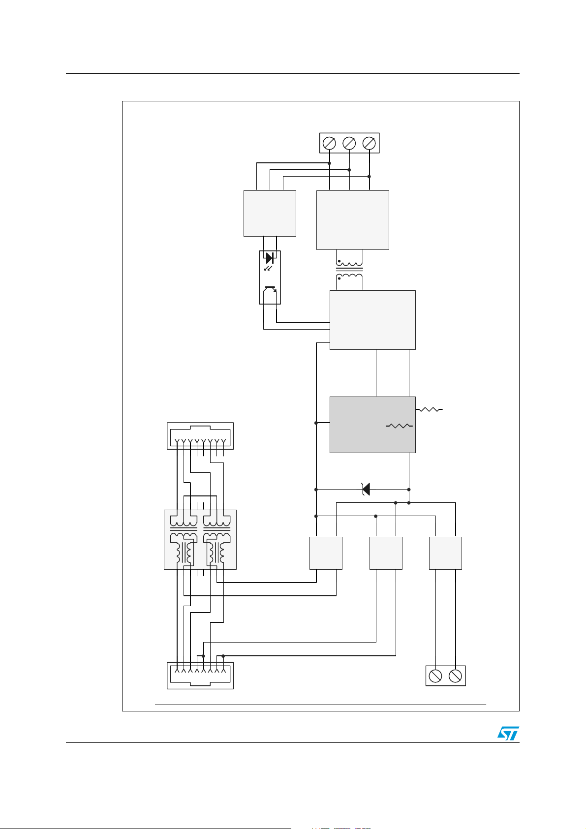
Figure 1. Block diagram of demonstration board PSAL06-17 rev 2
OUT GND
+3.3v
+12v
ISOLATED
POWER
TB2
1
2
3
TL431
FEEDBACK
1
23
\
4
STPS2L40U
STPS3150U
RECT IFI ER
POWER
CONVERTE R
OUT P UT
SMAJ188
ST D5N20T 4 FET
2345678
1234567
11
12
13
14
15
16
8 1
POE-PD
TRANSIENT
Power Good
I/F Chi p
STHS4257 L6565D Cont rol
CLA MP
SMAJ58A
1
V+
AC
BR2
4
Power Pos
ET HERNET
TO OTHER
EQUIPMENT
ISOLATED
89
ETHERNET
ISOLATION
TRANSFORMER
SIMPLEX T AP
SOURCING
POWER
UNUSED
PAIR
POWER
EQUIPMENT
10
1234567
ET HERNET
TO POWER
BR1
1
2
V-
V+
AC
AC
4
3
Po wer Ne g
IF NEEDE D
Classification
Signatu re
2
V-
AC
3
1
2
V-
V+
AC
BR3
TB1
AC
4
3
TEST
POWER
1
2
AUXILIARY
POWER I NPUT
8/32
Page 9
AN2487 Powered device demonstration board
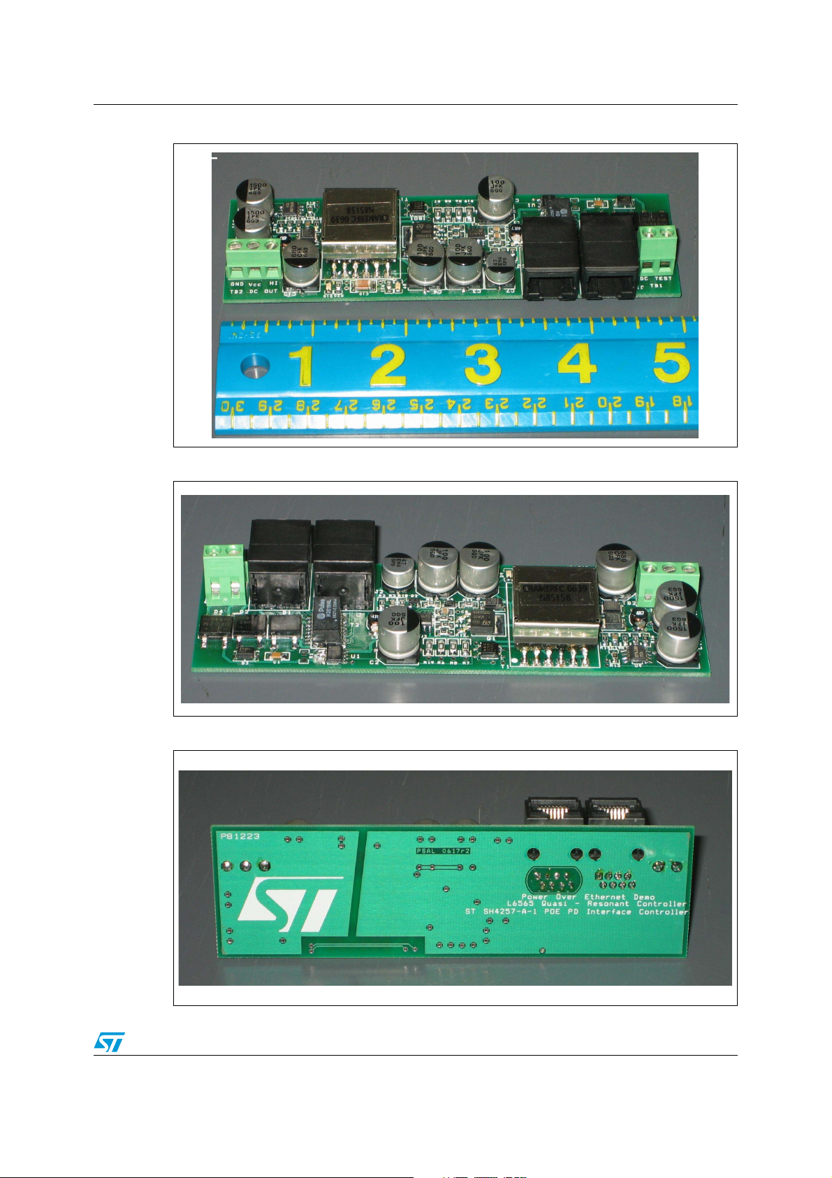
Figure 2. Front of demonstration board
Figure 3. Rear of demonstration board
Figure 4. Bottom of demonstration board
9/32
Page 10
Circuit descriptions AN2487
2
3 Circuit descriptions
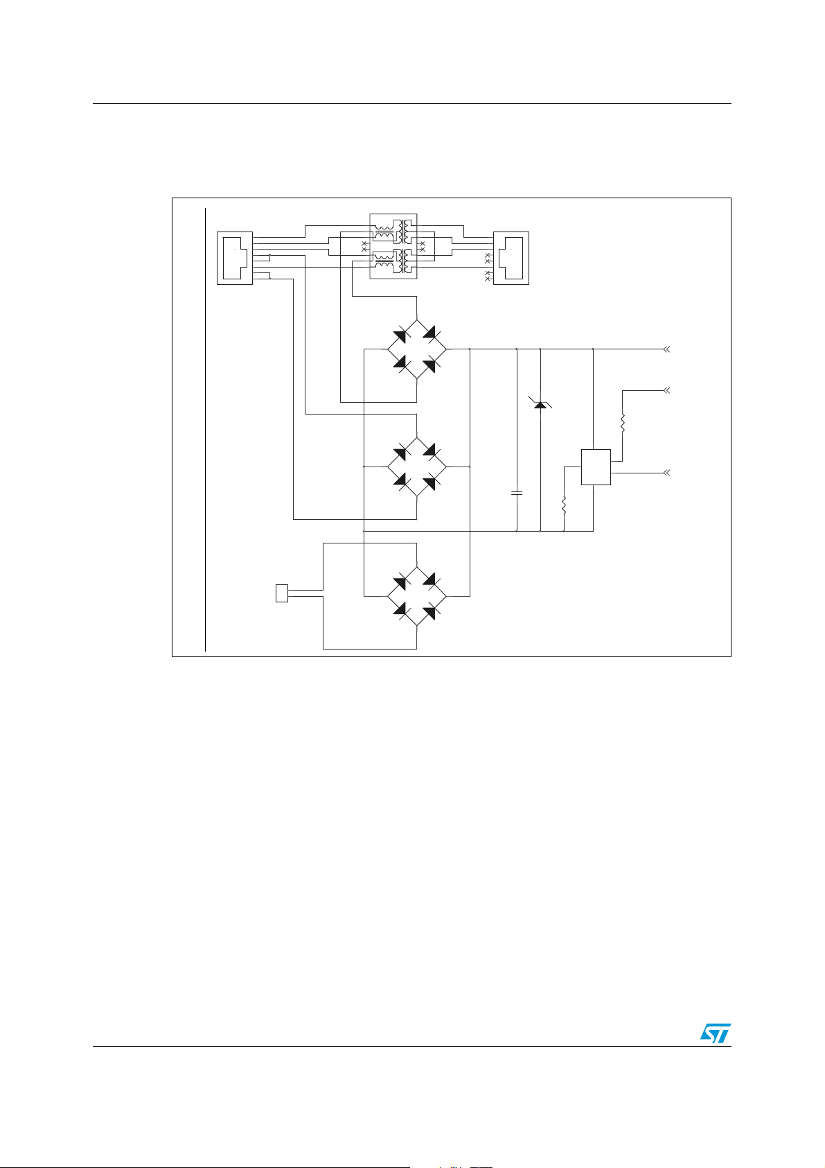
Figure 5. Test and Ethernet source connection circuitry
T2
J1
1
2
3
4
5
6
7
8
OVERHANG BOARD EDGE 0.062
RJ-45
TO POWER SOURCING EQUIPMENT UNPOWERED, ISOLATED, SIMPLEX LOOPBACK
16
15
14
13
12
11
10
POE Signal XFMR
1
2
3
4
5
6
7
89
32
D1
DF02M
J2
1
2
3
4
5
6
7
8
RJ-45
OVERHANG BOARD EDGE 0.062
J3
Phoenix 2 pin
3.1 Inputs
3.1.1 Power supplies
4 1
TO POWER CONVERTER, SHEET 2 OF
D3
SMAJ58A
C1
0.1uF
100V
A K
8
U1
V+
/PG
2
CLASS
RTN
V-
STHS4257A
4
12
R1
DNI
1/8W
1%
32
D2
DF02M
4 1
32
D4
DF02M
1
2
4 1
48V+
48V+
/PG
/PG
12
R2
100K
1/8W
6
48V-SW
5
48V-SW
There are three methods of powering the demonstration board:
1. Unused pairs (J1)
The unused twisted pairs in the Ethernet cable can carry power to RJ-45 pins 4 and 5,
and pins 7 and 8.
2. Simplex leads (J1)
The transformer windings are center tapped, and power is carried over the same pairs
as the signal leads. The DC power current balances out in the transformer - saturation
of the core does not occur, and the signals can pass. Power is drawn off the centertaps
(simplex leads) and signals are coupled to another winding.
3. Auxiliary DC input (TB1)
For convenience, this input method is provided for test and evaluation. Each input is
sent through its own bridge rectifier so that it is polarity insensitive.
10/32
Page 11

AN2487 Circuit descriptions
3.1.2 Transient protection
A 58 V Zener diode (D3) is placed across the DC bus so that it clamps all inputs to slightly
more than that value. ESD and connection transients then cannot harm downstream
circuitry.
3.1.3 Input capacitor
The 802.3af specification requires at least 0.05 µF of capacitance for the maintain power
signature. 0.1 µF is installed at C1. This capacitor must be rated for at least 90 volts.
3.2 STHS4257 powered device interface controller
3.2.1 Sequence of operation
During startup (connection of PD or power-up of a PSE output), a reduced input voltage is
used to identify the loads requiring power. Between -2.8 V and -10 V, an incremental load
slope of 25 k indicates that the load is requesting power. This is called the PoE signature
resistance.
3.2.2 POE Signature resistance
The STHS4257 powered device interface controller generates the 25 kΩ signature
resistance slope internally. No external resistor is required. Note that there is a Signature
Disable function on the chip, which is not used in this design. The signature disable function
can be used to disable power from the PSE if the powered device is receiving its power from
another source.
3.2.3 Classification
Between -15.5 and -20 V the load current indicates a power classification. Optionally, the
Powered Device can inform the power sourcing equipment (PSE) to expect loading in a
defined range. A precision resistor could be added at the R1 location to set Classification
Current. The resistor was not installed in the demo board, so the board reports Class 0
(zero), informing the PSE that power may be required over any part of the full 0.44 W to
12.95 W load range. Table 3 in the STHS4257 datasheet and Tables 33-3 and 33-4 in the
IEEE 803.2af specification show the defined ranges and resistor values. Tab le 1 below
combines the information.
Table 1. Power classes and class identification
Class Power range Notes Classification current R1 value
0 0.44 to 12.95 W Default 0 to 4 mA Open
1 0.44 to 3.84 W Optional 9 to 12 mA 124 Ω
2 3.84 to 6.49 W Optional 17 to 20 mA 68.1 Ω
3 6.49 to 12.95 W Optional 26 to 30 mA 45.3 Ω
4 Reserved Reserved 36 to 44 mA 30.9 Ω
11/32
Page 12

Circuit descriptions AN2487
Two methods of determining the classification are supported:
● Voltage between -15.5 and -20 V is applied and the current is measured (IEEE803.2af
compliant); or,
● Current is applied and voltage measured (obsolete, requires multiple test currents).
The STHS4257 supports both methods -- it acts as a current sink. If voltage is applied and
current measured, the classification is determined in a single step.
If a current between the classification ranges is applied, the voltage across the device will be
either less than 15.5 V or greater than 20 V. Stepping the current between ranges allows
determining the classification.
Because of the relatively high dissipation in the chip at the higher classes, the classification
time is specified by IEEE 802.3af at 75 ms (maximum).
3.2.4 Startup sequence
If the signature (and classification, if implemented) tests indicate that power should be
applied to the PD, the PSE will apply the available voltage to the ethernet cable with the
current limited to 400 mA. (If the source is in current limit for more than 50ms, the load is
disconnected.) This allows charging of the power converter input capacitors.
Action of the PD is then determined by the voltage at the STHS4257 input and the state of
its internal current limiter.
If the input voltage to the STHS4257 is below 30 V, nothing happens; no current is supplied
to the power converter.
If the input voltage is above 42 V, the STHS4257 turns on, supplying current-limited power to
the power converter input.
The power converter requires capacitance at its input, usually in the range from 50 to
300 µF. This capacitance (C2, 3, and 4) is charged to the input voltage by the internal
current limiter of the STHS4257.
When the capacitor charging current falls to a predetermined value, the capacitor is
assumed to be charged. At this point, input and output voltages of the STHS4257 are nearly
equal, and the current limit function is replaced by a low-resistance switch.
When the switch turns on, the /Power Good signal is also turned on, pulling pin 6 to V
This signal is used to start the power converter.
Two events can stop the STHS4257 startup: overtemperature and undervoltage. If either
event occurs, the /Power Good signal goes high impedance (open circuit), and the FET
connection from V
IN
to V
(pins 4 and 5) is opened.
OUT
If neither event occurs, the /Power Good signal turns on Q2, which enables current to trickle
through R5 to charge C7 in the housekeeping supply of the power converter. Approximately
40 milliseconds later, C7 is charged to the L6565's startup voltage and the converter starts.
3.2.5 Maintain power signature (MPS)
The converter must maintain two signatures if the PSE is to continue supplying power:
● DC MPS - Current of at least 10 mAdc drawn from the PSE for 60 ms out of any 360 ms
period. Dropouts cannot exceed 300 ms.
● AC MPS - Impedance less than 27 K at 500 Hz, >2.5 V test signal
The PSE can optionally ignore either the DC or AC MPS. The PD must present both.
OUT
.
12/32
Page 13

AN2487 Circuit descriptions
3.3 Power converter operation
The following sections refer to the power converter schematic shown in Figure 6.
ST's L6565 (U3) is a transition-mode peak-current controller that drives the FET (Q1) of a
flyback converter in response to feedback signals from the converter output and a bootstrap
winding.
An excellent description of the converter operation is available in the L6565 datasheet, with
further detail in ST application note AN1326. Additional design examples are shown in
application notes AN1376, AN1439, and AN2252. A design spreadsheet is also available. It
is strongly recommended that the designer consult these resources.
3.3.1 Input filtering
The power converter has a discontinuous input current. The AC component of this current is
supplied locally, by capacitors C3 and C4. C1 and L2 filter the input voltage so that the
power source is not polluted.
3.3.2 Startup
When the converter initially starts, the L6565 controller (U3) runs from the charge on C7.
This charge is quickly depleted, however, and a second power source must start before U3
starves.
One of T3's secondaries is used to bootstrap housekeeping power to the L6565. Pin 12 of
Transformer T3 feeds R11 and D5 to provide enough current for normal operation.
At Q1's first turn-on, current begins to rise linearly (several microseconds) in T3's primary,
pins 2 and 3. The current is sensed by the L6565 as the voltage drop across R6, 7, 8, 10,
and 19. At the threshold set by the L6565 (more about this in Section 3.3.3: Regulation), the
gate drive is removed and the magnetic field generated by T3's primary current is picked up
by its secondaries, and fed to the capacitors C7, C11, C12, and C15. The cycle repeats as
soon as the field stored in the transformer is depleted, repeating until the capacitors are
charged to the desired voltages.
3.3.3 Regulation
Eventually (several milliseconds) the load capacitors charge to the desired voltages. The
voltage on C11 is monitored by U4, and when U4 conducts sufficiently, it turns on
optoisolator ISO1.
On the left side of the isolation barrier, ISO1 pulls down on U3's compensation node (pin 2).
Peak primary current is controlled directly by the error in output voltage of the 3.3 V output,
and inversely by the input voltage. A higher input voltage means that the converter spends
less time charging T3's inductance, resulting in a higher power output for the same peak
current. This is compensated by U3's internal multiplier, which reduces the peak current
setting for higher voltage inputs; so the system gain, current limit and operating point remain
roughly constant.
Divider R3-R4 sets the voltage input to the L6565's multiplier, which is used to compensate
for the faster transformer charge at high voltage. The voltage on pin 2, multiplied by (3 volts
less the voltage on V
), sets the shutoff point for the primary ramp current.
FF
13/32
Page 14

Circuit descriptions AN2487
Figure 6. Power converter circuitry
14/32
Page 15

AN2487 Circuit descriptions
3.3.4 Critical conduction operation
When close to or at full load, this converter operates on the boundary between continuous
conduction and discontinuous conduction. The magnetic field in the transformer is allowed
to completely collapse each cycle as the combined secondary currents drop to zero, then
the FET is turned on (with zero or very low voltage on its drain) to begin charging the
primary inductance.
The end-of-secondary-conduction point is detected at T3 pin 12. The voltage across the
winding is slightly above the voltage on C7, and will suddenly drop down through zero and
swing negative as the magnetic field in T3 collapses. This is detected by U3 pin 5 and used
to start the next cycle by driving the gate of Q1. R12 and the input capacitance of U3 pin 5
provide a slight tunable delay.
3.3.5 Outputs
Transformer T3 feeds two Schottky rectifiers for the 3.3 V and 12 V outputs. Regulation of
only the 3.3 V output is regarded as sufficient, as the 12 V output is seldom used for critical
loads. Cross-regulation is sufficient.
3.3.6 Miscellaneous component functions
● T1 provides a small amount of common-mode filtering and isolates the Ethernet input
and output connectors.
● R2 limits the base current to Q2.
● R18 insures that Q2 leakage is minimal if it is not being driven.
● R11 and C7 provide a small filter that removes the leakage spike when current
transfers from the primary to the secondary.
● R9 prevents oscillation of Q1 due to trace and lead inductance. It also slows slightly
Q1's turnoff transient, softening the noise-producing edges.
● C10 short-circuits switching noise current that could be coupled from the drain of Q1
through the transformer capacitance to output ground.
● L1 reduces ripple in the 3.3 V output to digital circuit requirements; less than 2% P-P,
with C11 and C12.
● C15 filters the 12 V output. The ripple and spike noise on this output is relatively high;
the output is still suitable for driving relays, downstream power converters, or
illumination.
● R13 insures that ISO1's LED can completely turn off. If not present, the approximate ½
mA keep-alive current required by U4 would partially turn on the isolator.
● R14 limits the current into the isolator.
● R16 and R16 divide the 3.3 V output down to 2.495 V so U4 can compare that voltage
to its reference.
● R15 and C19 stabilize the control loop by slowing down U4's response to error signals.
● D9 (yellow LED), powered by R21, indicates that the STHS4257 chip has passed
power to the power converter.
● D10 (green LED), powered by R20, indicates that the power converter is up and
running.
15/32
Page 16

Circuit descriptions AN2487
3.4 Transformer details
The transformer used in the STEVAL-TSP001V1 demo board is Cramer part number
N85158. The secondary turns counts can be changed to accommodate other voltages if
required. Please contact the manufacturer for more information.
● Construction:
– Core: EFD20, any power material. Gap for 164 µH total primary inductance, pins 2
and 3 (A sub L = 63 nH/T^2)
– Bobbin: Pin Shine EFD-20 12-pin SMT bobbin
● Windings:
– Winding 1: 1/2 primary; 26 turns 28AWG; start pin 11; finish pin 3; tape 1 layer 1.5
mil Mylar
– Winding 2: 3.3 V secondary; 6 turns 3x 28AWG, 1 strand per section, trifilar
a) Section A: start pin 5; finish pin 8
b) Section B: start pin 6; finish pin 9
c) Section C: start pin 5, finish pin 9
● Winding 3: 3.3 V to 12 V secondary section; 14 turns 28AWG Start pin 7 finish pin 6
● Tape 1 layer 1.5 mil Mylar
● Winding 4: Bootstrap; 26 turns 32AWG; start pin 12; finish pin 1
● Winding 5: 1/2 primary; 25 turns 28AWG; start pin 2; finish pin 11
● Tape 2 layers 1.5 mil Mylar to protect windings
The transformer was overdesigned so that it could operate at higher power levels if required
in the future.
16/32
Page 17

AN2487 Electrical characteristics
4 Electrical characteristics
4.1 Test setup
Figure 7 shows a diagram of the loads and power supplies used for the test setup.
Figure 7. Test setup
INPUT
AMMETER
R1
(2) 10 ohms 1%
S?
SW-SPST
R2
2
TB1
TEST I NP UT
INPUT
VOLTMETER
1
DEVICE UN DER TESTDC PO WER SUPP LY 0-6 0V DC LO AD 0-2A DC LOAD 0- 2A
12V
VOLTMETER
3.3V
VOLTMETER
TB2
DC OUTPUT
3.3V
AMMETER
3.3V LOAD
123
4.2 STHS4257 powered device interface controller
4.2.1 Signature current
Figure 8 compares the incremental slope and linearity of the signature resistance to the
ideal slope and the limits. The limiting resistances were plotted, and then the limiting
resistance curves and the data for the chip were shifted vertically to match the lower limit of
the measurement range. Error can then be measured at the upper end of the measurement
range.
Linearity of the slope does not appear to be an issue within the measurement range.
Figure 8. Signature resistance slopes
12V
AMMETER
12V LOAD
Signature Current
600
500
Slope Measurem ent Range
400
300
200
Input Current, Mi croamps
100
Shifted ST Data
Lower Resistance Limit
Upper Resistance Limit
0
024681012
Input Voltage
17/32
Page 18
Electrical characteristics AN2487
4.2.2 Classification current
Ta bl e 2 shows the classification current for the values of classification resistors shown (R1 in
Figure 5).
Table 2. Classification current
Class 01234
Watts available at PSE
connector
Specified R Open 124 Ω 68.1 Ω 45.3 Ω 30.9 Ω
Measured R used Open 124.1 Ω 67.8 Ω 45.3 Ω 30.8 Ω
Specified current range 0 to 5 mA 8 to 13 mA 16 to 21 mA 25 to 31 mA 35 to 45 mA
STSH4257-
A-1 test
results
Current at
15.5 V
Current at
20.5 V
All the currents are well within the specification limits.
4.2.3 Undervoltage lockout
The startup and shutdown voltages, at which the chip starts the load or turns the load off,
were measured. Results are shown in Ta b le 3 .
Table 3. PD Startup and shutdown voltages
Startup Shutdown
37.01 V 31.9 V
(future)
15.4 W 4.0 W 7.0 W 15.4 W
0.243 mA 10.11 mA 18.28 mA 27.22 mA 39.74 mA
0.278 mA 10.15 mA 18.31 mA 27.25 mA 39.73 mA
Treat as
class 0
These values are the board input voltages at which the STHS4257A1 chip enables and
disconnects the power converter. The data was taken with no load on the power converter
output. Startup occurs shortly after the /Power Good signal goes low, when the Vdd
capacitor charges to the L6565's startup voltage (12.5 to 14.5 volts). Shutdown occurs when
the STHS4257A1 chip disconnects the converter from its power source and the input
capacitors discharge.
18/32
Page 19

AN2487 Electrical characteristics
4.3 Powered device supply solution
The following properties were verified by testing the demonstration board against IEEE
802.3af, section 33.C.5 specifications.
4.3.1 Current draw at low input voltage
Table 4. Input current at 30V
Input voltage Input current Specification I
30.0 0.273 mA 1.14 mA
The system is not allowed to draw significant power if its input is below 30 V.
4.3.2 Power Good signal and capacitor charging current
Figure 9. 42 V input Figure 10. 57 V input
● Upper trace, channel 1: Power Good signal relative to power converter input negative
● Lower trace, channel 2: Input current to PD
max
4.3.3 Discussion
On the lower trace, two distinct regions are visible.
The first is the charging of the power converter input capacitors. The current is limited to a
low value (around 140 mA) by the STHS4257A1 chip. After these capacitors charge, the
Power Good (channel 1) signal drops, allowing the converter's Vcc capacitor to begin
charging. A short time later, the converter starts, drawing significant current (approximately
350 mA) while it charges its output capacitors.
4.4 Startup loading on the power sourcing equipment
According to the specification, once power is applied to the PD, the PSE must shut down if
the load current exceeds 400 mA for more than 50 milliseconds. After this startup transient,
the overcurrent trip point is reduced to 350 mA.
19/32
Page 20

Electrical characteristics AN2487
The traces in Figure 11 and Figure 12 were taken with 20 ohms in series with the demo
board's input to simulate cable resistance.
Figure 11. Full-load startup input current with
Figure 12. Full-load startup input current with
cable resistance - 44 V source, 37 V
at PD
● Channel 1: DC input current, 100 mA/division
● Channel 2: 12 V output voltage, 10 V/division
cable resistance - 57 V source,
input
Starting at the first division from the left, note the capacitor charging current, limited by the
STHS4257A1 chip. Until the power converter's input capacitors are charged, this chip does
not permit the converter to start. This prevents the sudden application of both load current
and capacitor charging current at the same time, which would overload the PSE.
The STHS4257A1 chip dissipates considerable heat during the charging of the converter's
input capacitors. It does rather well with the 300 µF capacitance used in the demo board.
Note that 300 µF is a rather high value for the input capacitors, chosen to stress the chips.
However, once the capacitors are charged, (and before the converter starts) the chip turns
on an internal FET switch to reduce losses. Current limiting ceases; the converter is
connected directly to the input power.
After about 3.5 divisions the power converter starts, drawing current from its input capacitors
to charge its output capacitors and to supply the resistive test load. The energy required to
charge the converter's output capacitors can be clearly seen as an overshoot in the input
current (top trace).
Note also that the STHS4257A1 chip must supply input capacitor charging current for a
longer period at 57 V, because it charges the capacitors to a higher voltage at the same
current. The output capacitor charging spike is also shorter at 57 V, because more energy is
stored in the input capacitors. Also note that the converter draws significantly less current at
57 V than it does at 37 V.
4.4.1 Maintain power signature
This design does not meet the DC maintain power signature current of 10 mA minimum.
This could easily be corrected (if necessary) by increasing the LED current or preloading the
outputs, but it is assumed that some load will be present at the converter's output. Input
current with no load was measured over the operating voltage range.
20/32
Page 21

AN2487 Electrical characteristics
Figure 13. No load current - DC maintain power signature
10.6
10.4
10.2
10
9.8
9.6
9.4
No-Load Current, mA
9.2
9
8.8
40 45 50 55 60
Input Voltage
Note that most of the no-load current is due to the presence of the two LEDs on the board.
The AC maintain power signature is present by design. Small variations in input voltage will
draw capacitive current from the PD's large input capacitors.
Both the DC and AC maintain power signatures must be present for compliance with the
IEEE specification.
4.5 STHS4257A1 voltage drop under load
The load power was trimmed so that the input current was 350 mA and the voltage drop
between the STSH4257-A-1 Vout (pin 5) and Vin (pin 4) was measured.
Table 5. Voltage drop under load, worst case input current
IDC measured V drop measured Power loss
0.35 A 260 mV 91 mW
Discussion
This represents an efficiency loss of 0.61%, which is quite negligible.
4.6 Input current limit vs. input voltage
The STHS4257A1 chip limits the input current to 350 mA. The power converter current limit
is set just slightly above that level, so that (if desired) the supply can be used at higher load
currents with the source voltage at the high end of its range. At 350 mA and 57 V, with no
Ethernet cable resistance present, the total input power available is almost 20 W.
The converter section's input current limit is flattened over the input voltage range by the
voltage feed-forward scheme. See the L6565 literature for a thorough explanation.
21/32
Page 22

Electrical characteristics AN2487
4.7 Characteristics of entire system
4.7.1 Output vs. input voltage
As can be seen from the figures below, there is almost no sensitivity to input voltage. This is
a characteristic common to all current-mode controlled converters.
4.7.2 Cross regulation
The following graphs should be self-explanatory.
Note that there is almost no variation with input voltage.
Figure 14. Cross regulation, 42 V In, 12 V at
half load, 3.3 V load varied
Figure 15. Cross regulation, 42 V In, 3.3 V at
half load, 12 V load varied
14
12
10
8
6
4
Out put Volt ages
2
0
0 0.2 0.4 0.6 0.8 1
3.3V Lo ad, Am ps
12V Output
3.3V Output
Figure 16. Cross regulation, 50 V In, 12 V at
14
12
10
8
6
4
Out put Vol tages
2
0
half load, 3.3 V load varied
12V Output
3.3V Output
00.20.40.60.81
3.3V Lo ad, Am ps
Figure 18. Cross regulation, 57 V In, 12 V at
half load, 3.3 V load varied
14
12
10
8
6
4
Out put Vo ltages
2
0
0 0.2 0.4 0.6 0.8 1
12V Lo ad, Am ps
12V Output
3.3V Output
Figure 17. Cross regulation, 50 V In, 3.3 V at
half load, 12 V load varied
14
12
10
8
6
4
Out put Volt ages
2
0
0 0.2 0.4 0.6 0.8 1
12V Lo ad, Am ps
12V Output
3.3V Output
Figure 19. Cross regulation, 57 V In, 3.3 V at
half load, 12 V load varied
14
12
10
8
6
4
Output Voltages
2
0
00.20.40.60.81
3.3V L oad, A m ps
12V Output
3.3V Output
22/32
14
12
10
8
6
4
Output Volt ages
2
0
00.20.40.60.81
12V L oad, A m ps
12V Output
3.3V Output
Page 23

AN2487 Electrical characteristics
The graphs above were run out to 0.8 A to show that loading can be traded off between the
two outputs with very little effect on output voltage. Note, however, that at very light loads the
cross regulation suffers. If light load operation is required, pre-loads may be necessary.
4.7.3 Startup and shutdown
Figure 20. 42 V full load startup Figure 21. 57 V full load startup
● Channel 1 = 12 V output
● Channel 2 = 3.3 V output
A slight voltage overshoot is visible as the control loop comes into play. This was not
regarded as serious enough to require correction.
Figure 22. 57 V shutdown full load
● Channel 1 = 12 V output
● Channel 2 = 3.3 V output
23/32
Page 24

Electrical characteristics AN2487
4.7.4 Transient response
Half load to full load transients were applied to the tested output with 50 V at the input. 16
sweeps were averaged by the oscilloscope to remove noise, which would otherwise obscure
the traces.
Figure 23. 3.3 V half-full transient, 12 V at half
load
Figure 24. 12 V half-full transient, 3.3 V at half
load
● Channel 1 = 12 V output
● Channel 2 = 3.3 V output
4.7.5 Overload characteristics
The STHS4257A1 limits the supply input current, thereby limiting the power to all outputs. If
the current drawn by the converter exceeds 350 mA the STHS4257A1 will shut off and
attempt to restart. As it continues to repeatedly recharge the power converter's input
capacitors, it will shut down thermally.
The 12 V output is well protected from overload as it carries the bulk of the output power. In
the short term, if it is sufficiently overloaded, the output voltage will fall on all windings of the
transformer, including the bootstrap voltage for the L6565. If the bootstrap voltage goes low
enough, the L6565 will shut itself off. It will attempt to restart when the bootstrap capacitor
gets recharged to the L6565 startup voltage, and then turn off again.
If the 3.3 V output is shorted, the mechanism above will protect the unit. However, the 3.3 V
output is not well protected against overload because it does not draw a large portion of the
input power. It can supply well over its rated current for short terms, but if an overload
remains in place the 3.3 V Schottky diode, the 3.3 V transformer winding, and the small filter
choke will be overstressed.
4.7.6 Efficiency
● Full load = 78.2%
● Half load = 76.5%
Note that these figures include the losses in the LEDs and the input diodes.
24/32
Page 25

AN2487 Electrical characteristics
4.8 Ripple and noise
Figure 25. Switching frequency ripple, two
cycles shown
● Channel 1 = 12 V output
● Channel 2 = 3.3 V output
4.8.1 Radiated EMI
For an idea of the noise level the converter will place on the Ethernet cable, the noise
between the two “ground” planes on the back of the PC board was measured. The signal
was run directly into the 50 Ω input of a spectrum analyzer. Please ignore the pass limit
notation.
Figure 26. Expanded switching transient
Figure 27. Spectrum of noise between output and input ground planes
The noise level peaks at 54 dB, about 1/2 mV, at approximately 63 MHz. Radiated noise
should not be a problem.
25/32
Page 26

Board layout AN2487
Appendix A Board layout
All board components are mounted on one side. All components are SMT except for
mechanically stressed connectors.
The board includes 2 mm creepage and clearance spacing between PSE-connected circuits
and load connected circuits (telecom network voltage - “TNV” isolation). The output RJ-45
connector (J2) is also isolated by 2 mm.
“Ground” planes are used on the bottom of the PC board, referenced to power converter
return (negative) and output common. This simplifies the layout and provides local
capacitive returns for noisy nodes such as the FET drain.
Design rules provide for 12 mil lines and 12 mil spaces.
Figure 28. Component placement
Figure 29. Top copper
26/32
Page 27

AN2487 Board layout
Figure 30. Bottom copper (mirrored)
Figure 31. Bottom of board (mirrored)
27/32
Page 28

Bill of materials AN2487
Appendix B Bill of materials
Table 6. Bill of materials
Qty Part type Designator Description Mfg & Mfg #
1 0.1 uF 100 V 1206 C1 Capacitor 0.1 µF 100 V *
1 4700 pF Y 1812 C10 Capacitor 4700 pF 1 kv Kemet C1812C472KDRACTU
2 1500 µF 6.3 V C11,C12 Capacitor 1500 µF 6.3 V Panasonic EEV-FK0J152P
1 680 µF 16 V C15 Capacitor 680 µF 16 V Panasonic EEVFK1C681P
1 3300 pF 0805 C18 Capacitor *
3 100 µF 63 V C2,C3,C4 Capacitor 100 µF 63 V Panasonic EEV-FK1J101P
1 47 µF 25 V C7 Capacitor 47 µF 25 V Panasonic EEV-HA1E470P
2 0.1 µF 0805 C8,C19 Capacitor *
1 0.01 µF 0805 C9 Capacitor *
3 BRIDGE DIP 1A D1,D2,D4 1 A dip bridge Diodes Inc DF1506DICT
1 LED GRN 0805 D10 Lumex SML-LXT0805GW-TR
1 SMAJ58A D3 Zener diode STMicroelectronics
1 1N4148W SOD123 D5 Diode *
1 SMAJ188 D6 Zener diode STMicroelectronics
1 STPS2L40U D7 Schottky diode 2 A 40 V STMicroelectronics
1 STPS3150U D8 Schottky diode 3 A 150V STMicroelectronics
1 LED YEL 0805 D9 Lumex SML-LXT0805YW-TR
1 PS2703-1_OPTO ISO1 Optoisolator SMT NEC PS2703-1-A
2 RJ45-8 FEMALE J1,J2 RJ45-8 socket Tyco-Amp 5557785-1
2 4.7 µH L1,L2 Inductor Tyco-COEV DU6629-4R7M
1 STD5N20T4 Q1 STMicroelectronics
1 MMBT5401 Q2 PNP transistor 150 V *
1 DNI 0805 R1 Classification resistor Not used, class 0 reported
1 10 5% 0805 R11 *
1 47 kΩ 5% 0805 R12 *
1 1.00 kΩ 1% 0805 R13 *
1 2.21 kΩ 1% 0805 R14 *
1 100 5% 0805 R15 *
1 3.24 kΩ 1% 0805 R16 *
1 10.0 kΩ 1% 0805 R17 *
1 100 kΩ 5% 0805 R2 *
1 4.7 kΩ 5% 0805 R20 *
28/32
Page 29

AN2487 Bill of materials
Table 6. Bill of materials (continued)
Qty Part type Designator Description Mfg & Mfg #
115 kΩ 5% 0805 R21 *
1 681 kΩ 1% 0805 R3 *
1 15.0 kΩ 1% 0805 R4 *
310 kΩ 5% 0805 R5,R10,R18 *
4 2.0 1206 R6,R7,R8,R19 *
1 22 5% 0805 R9 *
1 XFMR POE-15 T3 XFMR POE TAPPED SEC Cramer N85158
1 XFMR POE SIG T2 Pulse Eng. H2019
1 PHOENIX 2-PIN TB1 Connect2
1 PHOENIX 3-PIN TB2 Connect3
1 STHS4257-A-1 SO-8 U1 POE interface controller STMicroelectronics
1 L6565D SO-8 U3 TRANS. MODE CTLLR STMicroelectronics
1 TL431 SO-8 U4 TL431 PGM SHUNT REG STMicroelectronics
29/32
Page 30

Bibliography AN2487
Appendix C Bibliography
● IEEE 802.3af-2003, "Amendment: Data Terminal Equipment (DTE) Power via Media
Dependent Interface (MDI)"
● "Power over Ethernet Eases Design Implementations", Power Electronics Technology
magazine, November, 2003
● STMicroelectronics Application note AN1326, "L6565 QUASI-RESONANT
CONTROLLER"
● STMicroelectronics Application note AN1376, "25W QUASI-RESONANT FLYBACK
CONVERTER FOR SET-TOP BOX APPLICATION USING THE L6565
● STMicroelectronics Application Note AN1439, "EVAL6565N, 30W AC-DC ADAPTER
WITH THE L6565 QUASI-RESONANT PWM CONTROLLER
● STMicroelectronics Application note AN2252, "Zero-voltage switching and emitter-
switched bipolar transistor in a 3-phase auxiliary power supply"
30/32
Page 31

AN2487 Revision history
Revision history
Table 7. Document revision history
Date Revision Changes
04-Apr-2007 1 First issue
08-Aug-2008 2
Added order code to the Introduction on page 1.
Minor text changes throughout the document.
31/32
Page 32

AN2487
Please Read Carefully:
Information in this document is provided solely in connection with ST products. STMicroelectronics NV and its subsidiaries (“ST”) reserve the
right to make changes, corrections, modifications or improvements, to this document, and the products and services described herein at any
time, without notice.
All ST products are sold pursuant to ST’s terms and conditions of sale.
Purchasers are solely responsible for the choice, selection and use of the ST products and services described herein, and ST assumes no
liability whatsoever relating to the choice, selection or use of the ST products and services described herein.
No license, express or implied, by estoppel or otherwise, to any intellectual property rights is granted under this document. If any part of this
document refers to any third party products or services it shall not be deemed a license grant by ST for the use of such third party products
or services, or any intellectual property contained therein or considered as a warranty covering the use in any manner whatsoever of such
third party products or services or any intellectual property contained therein.
UNLESS OTHERWISE SET FORTH IN ST’S TERMS AND CONDITIONS OF SALE ST DISCLAIMS ANY EXPRESS OR IMPLIED
WARRANTY WITH RESPECT TO THE USE AND/OR SALE OF ST PRODUCTS INCLUDING WITHOUT LIMITATION IMPLIED
WARRANTIES OF MERCHANTABILITY, FITNESS FOR A PARTICULAR PURPOSE (AND THEIR EQUIVALENTS UNDER THE LAWS
OF ANY JURISDICTION), OR INFRINGEMENT OF ANY PATENT, COPYRIGHT OR OTHER INTELLECTUAL PROPERTY RIGHT.
UNLESS EXPRESSLY APPROVED IN WRITING BY AN AUTHORIZED ST REPRESENTATIVE, ST PRODUCTS ARE NOT
RECOMMENDED, AUTHORIZED OR WARRANTED FOR USE IN MILITARY, AIR CRAFT, SPACE, LIFE SAVING, OR LIFE SUSTAINING
APPLICATIONS, NOR IN PRODUCTS OR SYSTEMS WHERE FAILURE OR MALFUNCTION MAY RESULT IN PERSONAL INJURY,
DEATH, OR SEVERE PROPERTY OR ENVIRONMENTAL DAMAGE. ST PRODUCTS WHICH ARE NOT SPECIFIED AS "AUTOMOTIVE
GRADE" MAY ONLY BE USED IN AUTOMOTIVE APPLICATIONS AT USER’S OWN RISK.
Resale of ST products with provisions different from the statements and/or technical features set forth in this document shall immediately void
any warranty granted by ST for the ST product or service described herein and shall not create or extend in any manner whatsoever, any
liability of ST.
ST and the ST logo are trademarks or registered trademarks of ST in various countries.
Information in this document supersedes and replaces all information previously supplied.
The ST logo is a registered trademark of STMicroelectronics. All other names are the property of their respective owners.
© 2008 STMicroelectronics - All rights reserved
STMicroelectronics group of companies
Australia - Belgium - Brazil - Canada - China - Czech Republic - Finland - France - Germany - Hong Kong - India - Israel - Italy - Japan -
Malaysia - Malta - Morocco - Singapore - Spain - Sweden - Switzerland - United Kingdom - United States of America
www.st.com
32/32
 Loading...