

Page 1

AN2479
Application note
STA333ML demo board application note
Introduction
The purpose in this document is:
■ to describe how to connect the STA333ML demo board,
■ how to evaluate the demo board performance with electrical curve data,
■ how to avoid critical board and layout issues.
Application note can be configured to the 2.0 channels only. Both of the 2 channels are in
BTL mode. Each channel can deliver 20 W @ THD = 10% when Vcc = 18V and 8 load. It is
a total solution for the digital audio power amplifier in a TV application.
All the test items and graph data in this document are measured by audio precision
equipment. The test data shown in this document contains, for example, output power
versus Vcc, frequency response, THD+N versus frequency, THD+N versus output power,
FFT.
December 2006 Rev 1 1/42
www.st.com
Page 2

Contents AN2479
Contents
1 Test condition and connection of demo board . . . . . . . . . . . . . . . . . . . 3
1.1 Test condition . . . . . . . . . . . . . . . . . . . . . . . . . . . . . . . . . . . . . . . . . . . . . . . 3
1.1.1 Jumper, power supply, signal and interface setting . . . . . . . . . . . . . . . . . 3
1.1.2 Output configuration . . . . . . . . . . . . . . . . . . . . . . . . . . . . . . . . . . . . . . . . 3
1.2 Equipment requirement . . . . . . . . . . . . . . . . . . . . . . . . . . . . . . . . . . . . . . . 3
1.3 Connection method . . . . . . . . . . . . . . . . . . . . . . . . . . . . . . . . . . . . . . . . . . 4
1.3.1 Speaker jack connection . . . . . . . . . . . . . . . . . . . . . . . . . . . . . . . . . . . . . 4
1.3.2 Schematic . . . . . . . . . . . . . . . . . . . . . . . . . . . . . . . . . . . . . . . . . . . . . . . . 5
1.4 PCB Layout . . . . . . . . . . . . . . . . . . . . . . . . . . . . . . . . . . . . . . . . . . . . . . . . 5
1.4.1 Top view of PCB layout . . . . . . . . . . . . . . . . . . . . . . . . . . . . . . . . . . . . . . 5
1.4.2 Bottom view of PCB layout . . . . . . . . . . . . . . . . . . . . . . . . . . . . . . . . . . . 6
1.5 BOM list . . . . . . . . . . . . . . . . . . . . . . . . . . . . . . . . . . . . . . . . . . . . . . . . . . . 6
1.5.1 Test connection . . . . . . . . . . . . . . . . . . . . . . . . . . . . . . . . . . . . . . . . . . . . 7
2 Test curve report . . . . . . . . . . . . . . . . . . . . . . . . . . . . . . . . . . . . . . . . . . . . 8
2.1 Frequency Response . . . . . . . . . . . . . . . . . . . . . . . . . . . . . . . . . . . . . . . . . 9
2.2 THD versus frequency . . . . . . . . . . . . . . . . . . . . . . . . . . . . . . . . . . . . . . . 11
2.2.1 THD versus output power . . . . . . . . . . . . . . . . . . . . . . . . . . . . . . . . . . . 12
2.3 FFT . . . . . . . . . . . . . . . . . . . . . . . . . . . . . . . . . . . . . . . . . . . . . . . . . . . . . . 14
2.4 Cross talk . . . . . . . . . . . . . . . . . . . . . . . . . . . . . . . . . . . . . . . . . . . . . . . . . 23
3 Design guideline for PCB schematic and layout . . . . . . . . . . . . . . . . . 28
3.1 Schematic . . . . . . . . . . . . . . . . . . . . . . . . . . . . . . . . . . . . . . . . . . . . . . . . . 28
3.1.1 Main driver for components selection . . . . . . . . . . . . . . . . . . . . . . . . . . 28
3.2 Decoupling capacitors . . . . . . . . . . . . . . . . . . . . . . . . . . . . . . . . . . . . . . . 28
3.2.1 Output filter . . . . . . . . . . . . . . . . . . . . . . . . . . . . . . . . . . . . . . . . . . . . . . 28
3.3 Layout . . . . . . . . . . . . . . . . . . . . . . . . . . . . . . . . . . . . . . . . . . . . . . . . . . . . 31
4 Revision history . . . . . . . . . . . . . . . . . . . . . . . . . . . . . . . . . . . . . . . . . . . 41
2/42
Page 3

AN2479 Test condition and connection of demo board
1 Test condition and connection of demo board
1.1 Test condition
1.1.1 Jumper, power supply, signal and interface setting
1. JP1: format selection. 0
2. JP2: oversampling selection. 0 = 256 Fs, 1 = 384 Fs.
3. JP3: gain selection. 0 = 0 dB, 1 = +24 dB.
4. +3.3 V selection. Outer side = external +3.3 V, inner side = internal +3.3 V
5. Connect + voltage of 12 V DC power supply to +Vcc pin and negative to GND.
6. Connect + voltage of 3.3 V DC power supply to +3.3 V pin and negative to GND. If the
+3.3 V selection is set to the inner side, do not connect this wire.
7. Connect GUI AP interface board to the J3 connector of STA333ML demo board.
8. Connect the S/PDIF signal cable to the RCA jack on the interface board, The input
coming from the signal source such as Audio precision or DVD player.
9. The voltage range of the DC power supply for Vcc is from 5 V to 18 V.
(a)
= I2S, 1
(a.)
= left justified.
1.1.2 Output configuration
STA333ML demo board can be configured to 2.0 channels and do not require software
control. It is not necessary to connect the AP interface to the PC. When the power supply,
signal, interface and output have been setup, push the RESET button which allows the
STA333ML demo board to function.
1.2 Equipment requirement
● Audio Precision (System 2700) by AP Co., USA)
● DC power supply (With 5V to 18V)
● Digital oscilloscope (TDS3034B) by Tektronix
● PC
a. 0: connect to outer side, 1: connect to inner side.
3/42
Page 4
Test condition and connection of demo board AN2479
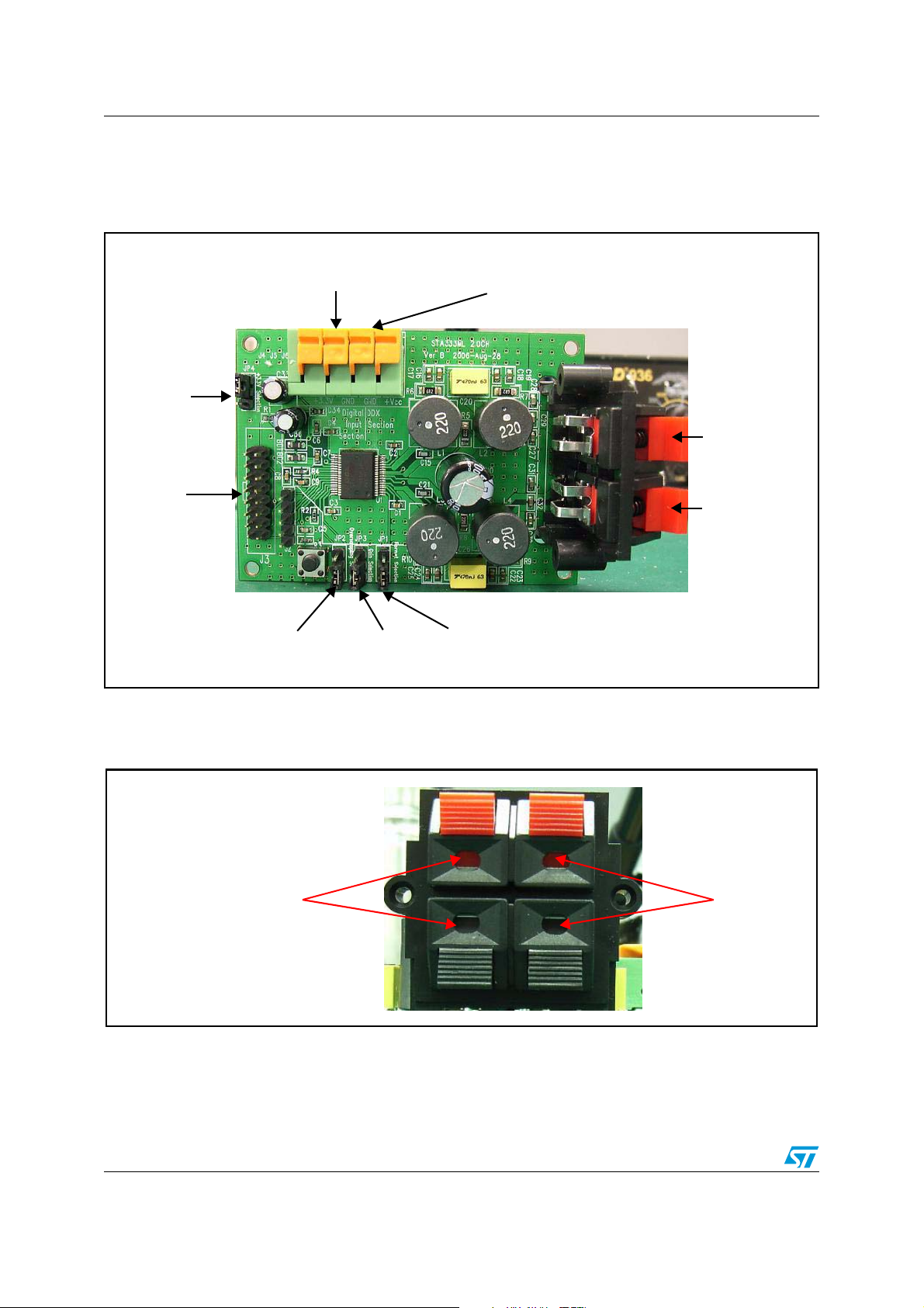
1.3 Connection method
Top view of demo board.
Figure 1. Block diagram
External 3.3 V
(not required if +3.3 V
selection is set to internal)
+3.3 V
selection
Vcc (5-18 V)
L_CH output
Connect to
interface board
Oversampling
selection
Gain
selection
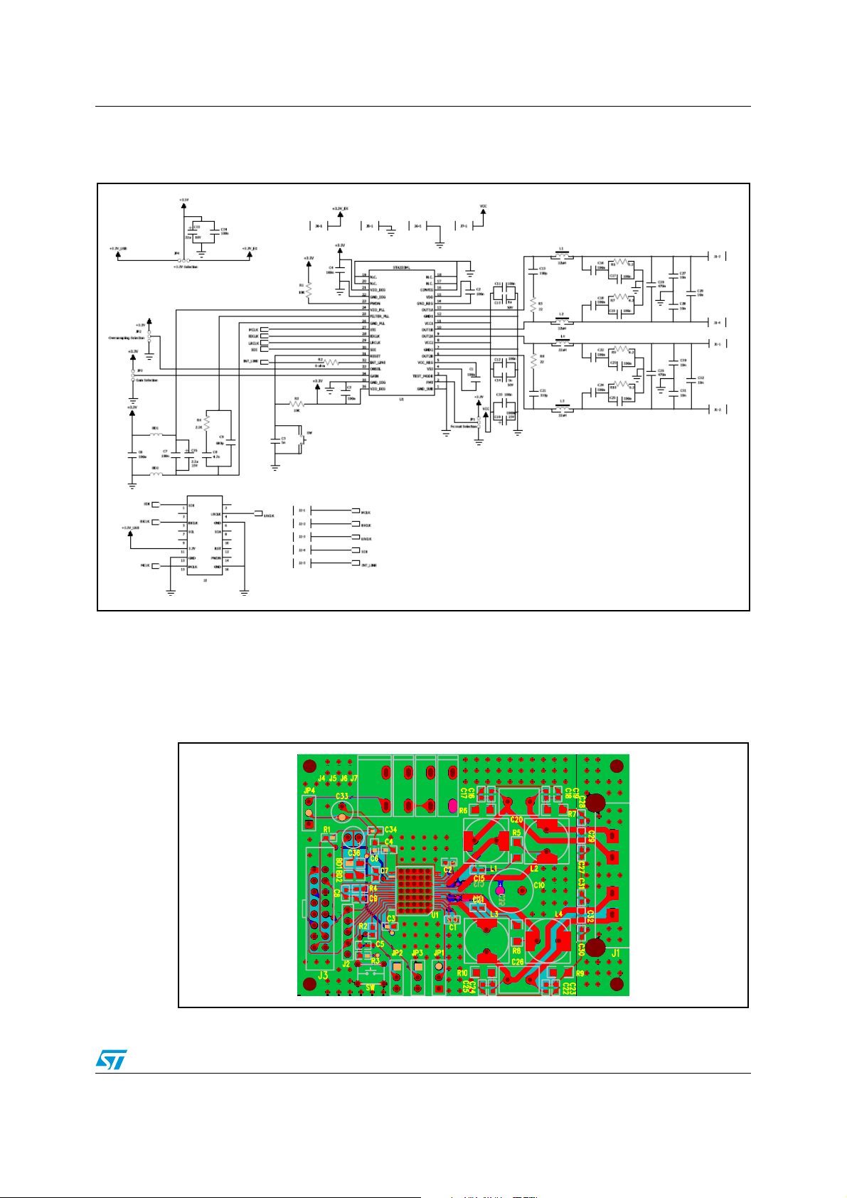
1.3.1 Speaker jack connection
Figure 2. Block diagram
R_CH output
Format
selection
L_CH outputR_CH output
4/42
Page 5
AN2479 Test condition and connection of demo board
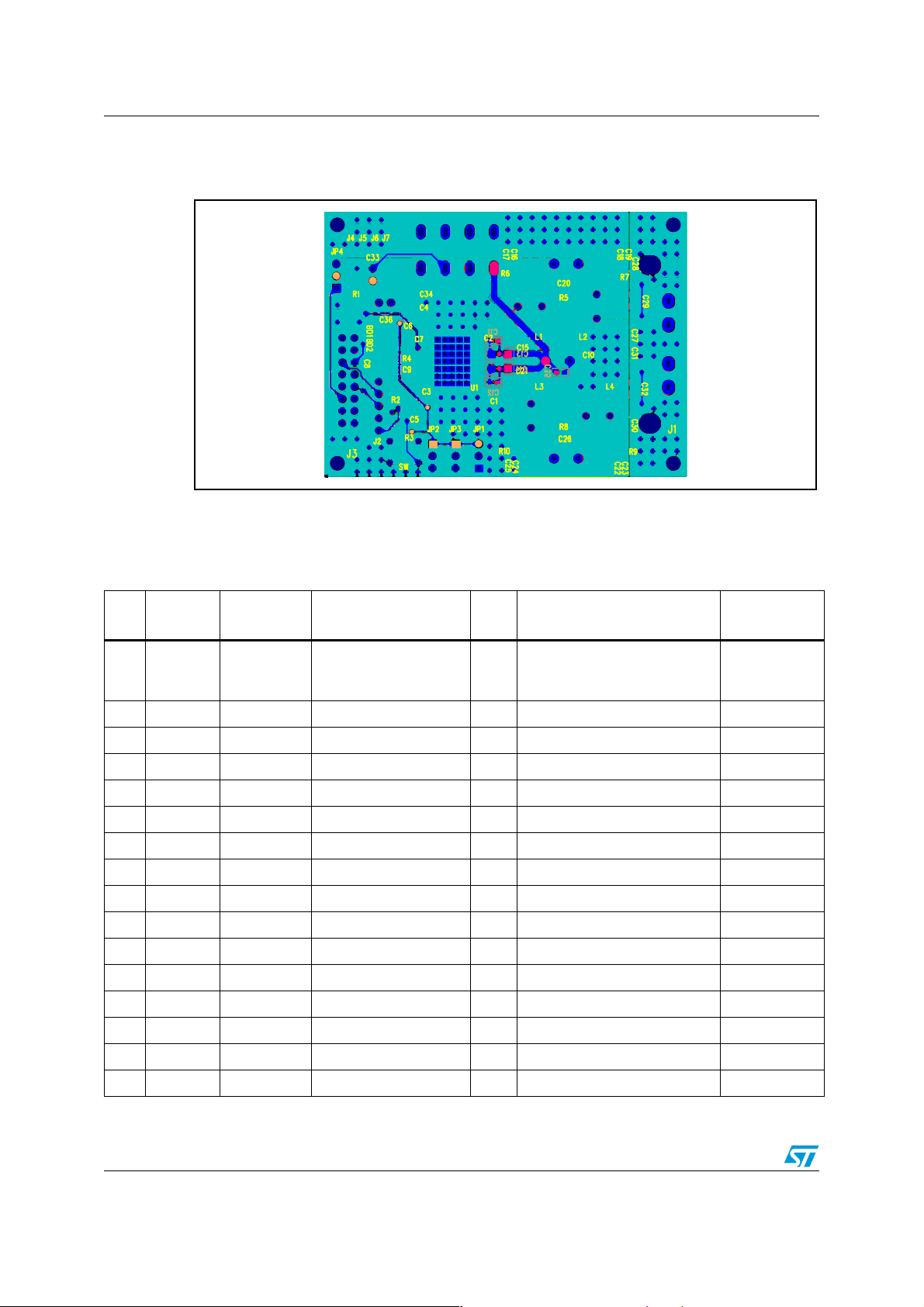
1.3.2 Schematic
Figure 3. Schematic diagram
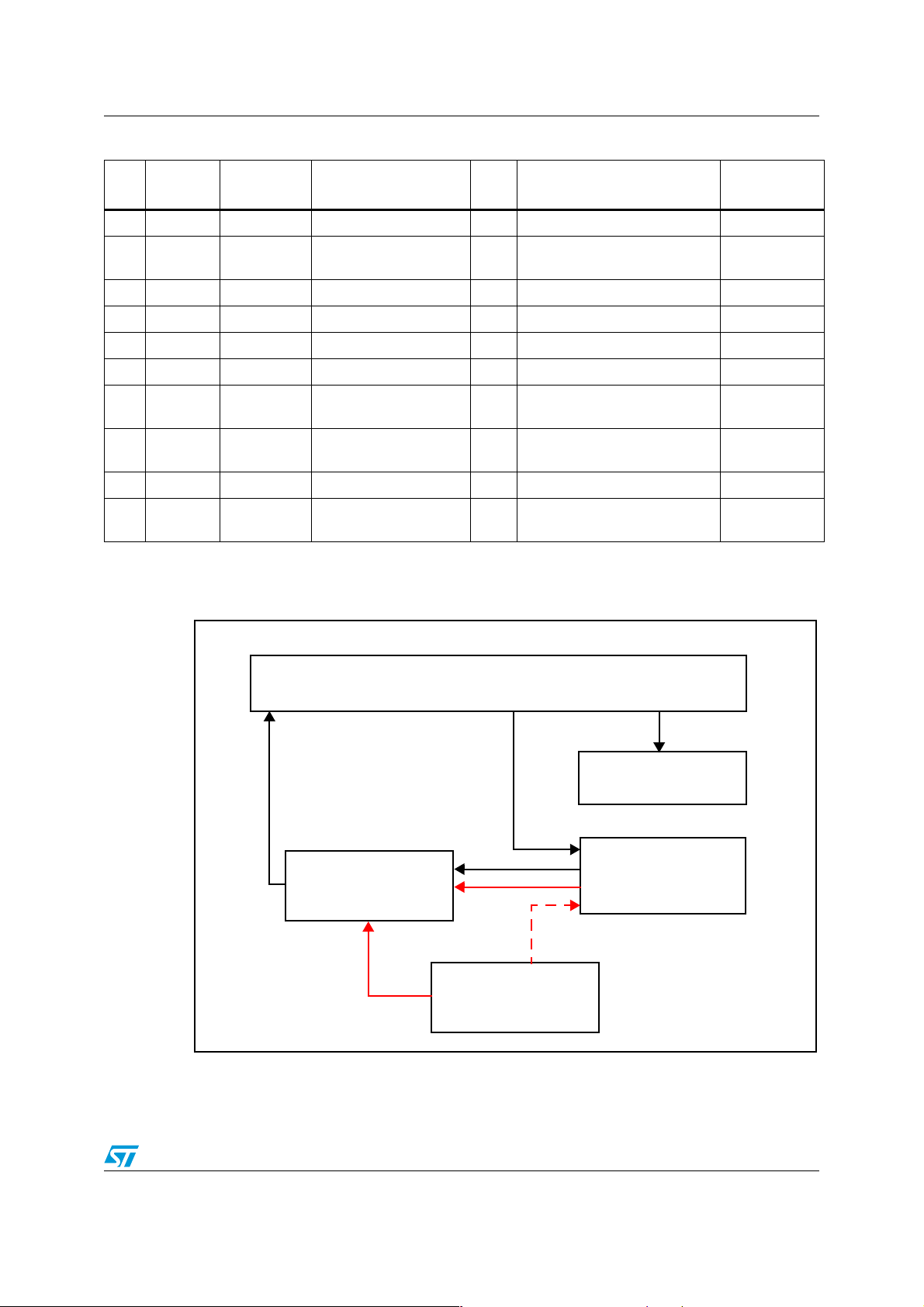
1.4 PCB Layout
1.4.1 Top view of PCB layout
Figure 4. Top layout
5/42
Page 6
Test condition and connection of demo board AN2479
1.4.2 Bottom view of PCB layout
Figure 5. Bottom layout
1.5 BOM list
Table 1. BOM
Item
no.
1 CCAP CCAP0603 100 n, 50 V, +/- 10 % 18
2 CCAP CCAP0603 1 n, 50 V, +/- 10 % 1 C5 Murata
3 CCAP CCAP0603 4.7 n, 50 V, +/- 10 % 1 C8 Murata
4 CCAP CCAP0603 680 p, 50 V, +/- 5 % 1 C9 Murata
5 CCAP CCAP0603 330 p, 50 V, +/- 10 % 2 C15, C21 Murata
6 CCAP CCAP0603 10 n, 50 V, +/- 10 % 6 C27, C28, C29, C30, C31, C32 Murata
7 CCAP CCAP1206 1 µ, 50 V 2 C13, C14 Murata
8 ECAP D = 10 mm 1000 µ, 25 V 1 C10 Rubycon
9ECAP D = 7mm22µ, 16 V 1 C33 Rubycon
10 ECAP D = 5 mm 2.2 µ, 25 V 1 C36 Rubycon
11 Chip bead L0805 600 ohm @ 100 MHz 2 BD1, BD2 Murata
12 CRES R0603 10 k +/- 5 % 2 R1, R3 Murata
13 CRES R0603 0 ohm +/- 5 % 1 R2 Murata
14 CRES R0603 2.2 k +/- 5 % 1 R4 Murata
15 CRES R1206 22 ohm +/- 5 % 2 R5, R8 Murata
Type Package Description Qty Reference code Manufacturer
C1, C2, C3, C4, C6, C7, C11,
C12, C16, C17, C18, C19, C22,
C23, C24, C25, C34, C35
Murata
16 CRES R1206 6.2 ohm +/- 5 % 4 R6, R7, R9, R10 Murata
6/42
Page 7
AN2479 Test condition and connection of demo board
Table 1. BOM
Item
no.
17 Test point Through hole 1 x 5 2.54 mm pitch 1 J2 Any source
18 Connector Through hole
19 Jumper Through hole 1 x 3 2.54 mm pitch 4 JP1, JP2, JP3, JP4 Any source
20 IC Through hole STA333ML 1 U1 ST
21 CAP Through hole 470 n 2 C20, C26
22 Connector Through hole WP4-15 1 J1 Song Cheng
23 Connector Through hole FFKDS/H1-5.08 3 J5, J6, J7
24 Connector Through hole FFKDSA1/H1-7.62 1 J4
25 COIL Through hole 22 µH 4 L1, L2, L3, L4 Kwang Sung
26
Type Package Description Qty Reference code Manufacturer
Ta c t
switch
2 x 8 2.54 pitch male
connector
Through hole 6 x 6 Tact switch 1 SW
1 J3 Any source
Phoenix
contact
Phoenix
contact
1.5.1 Test connection
Figure 6. Block diagram of test equipment
Output
to AP
STA333ML
demo board
From 5 V to 18 V
Audio precision equipment
S/PDIF
signal
2
I
S signal
Digital oscilloscope
TDS3034B Tektronix
(DC3V3)
(DC7V)
7V for LPT B’D
DC power supply
Monitor
AP interface
7/42
Page 8
Test curve report AN2479
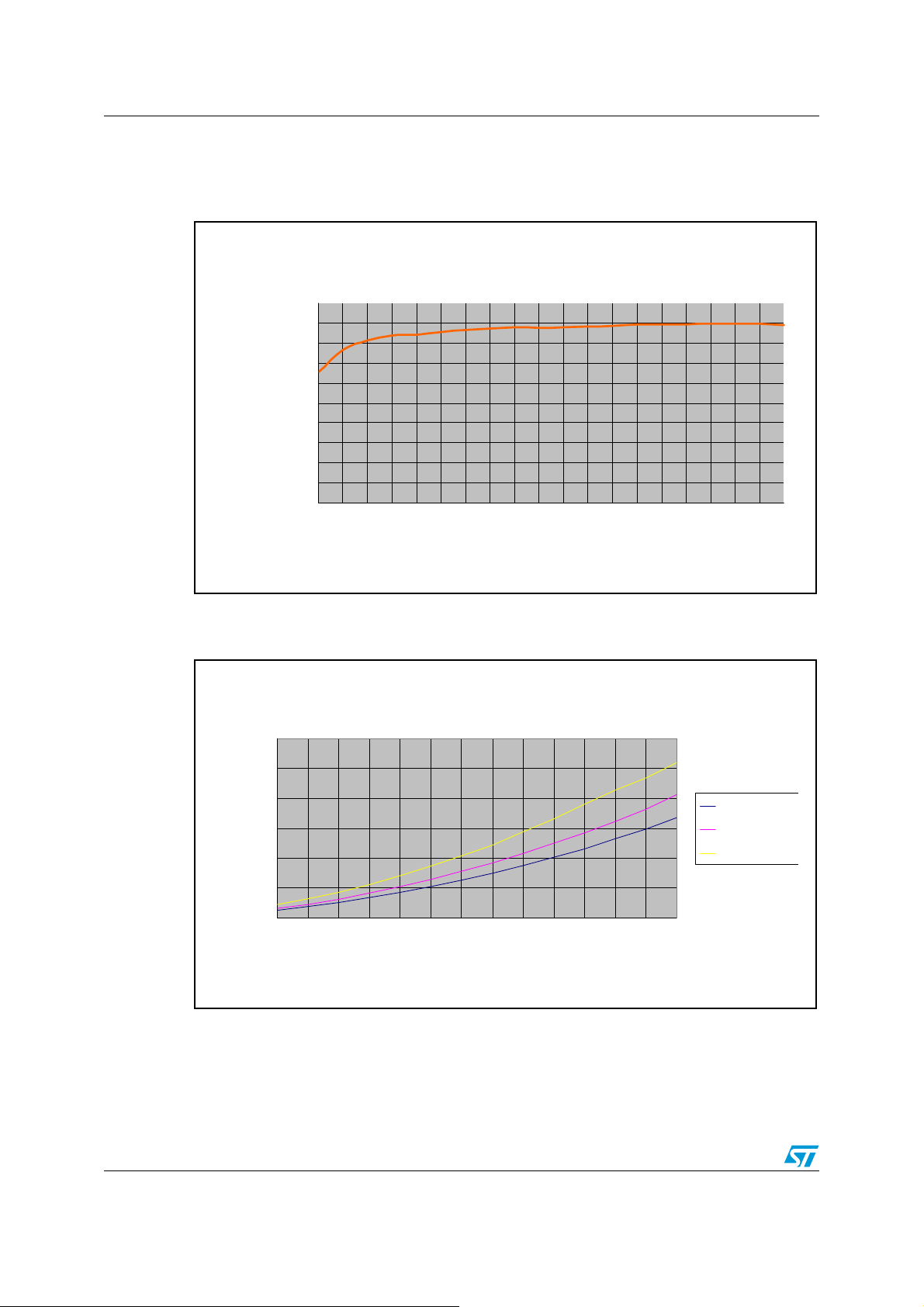
2 Test curve report
Figure 7. Efficiency versus output power
Efficiency
100.00
90.00
80.00
70.00
60.00
η(%)
50.00
40.00
30.00
20.00
10.00
0.00
1 2 3 4 5 6 7 8 9 1011121314151617181920
Condition: R LOAD =8 ohm; VCC=18 V
Figure 8. Output power versus Vcc
Output Power@1%THD vs. Vcc
30
25
20
15
10
5
Output Power (W)
0
5 6 7 8 9 10 11 12 13 14 15 16 17 18
Vcc (V)
Output Power (W)
Rl=8 Ohm
Rl=6 Ohm
Rl=4 Ohm
8/42
Page 9
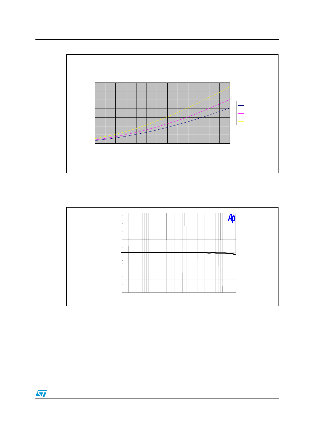
AN2479 Test curve report
A
k
k
Figure 9. Output power@10% THD vs. supply voltage
Output Power@10%THD vs. Vcc
35
30
25
20
15
10
5
Output Power (W)
0
5 6 7 8 9 101112131415161718
Vcc (V)
Rl=8 Ohm
Rl=6 Ohm
Rl=4 Ohm
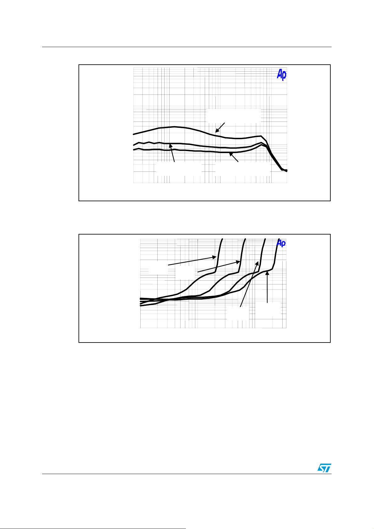
2.1 Frequency Response
Figure 10. 18 V 4 ohm 0 dB: Pout = 1 W@ 1 KHz filter: L = 10 uH, C = 1 uF
+3
+2
+1
d
B
+0
r
-1
-2
-3
20
50 100 200 500 1k 2k 5k 10
20
Hz
9/42
Page 10
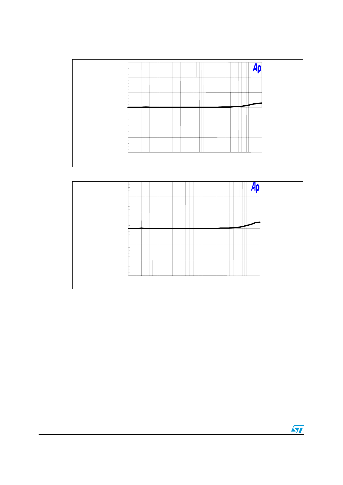
Test curve report AN2479
r
A
k
k5k10k
z
+3
A
k
Figure 11. 18 V 6 Ohm 0 dB: Pout = 1 W @ 1 KHz filter: L = 15 uH, C = 680 nF
+3
+2
+1
d
B
+0
-1
-2
-3
20 20
50 100 200 500 1k2
H
Figure 12. 18 V 8 Ohm 0 dB: Pout = 1 W @ 1 KHz filter: L = 22 uH, C = 470 nF
+2
+1
d
B
+0
r
-1
-2
-3
20
50 100 200 500 1k 2k 5k 10k
20
10/42
Page 11
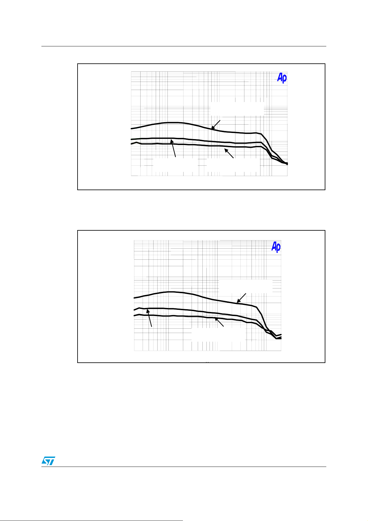
AN2479 Test curve report
020k
k2k5k10k
k
Figure 13. 6 Ohm Pout = 1 W
10
5
2
1
0.5
%
0.2
0.1
0.05
0.02
0.01
2
50 100 200 500 1
Vcc=5 V
Vcc=18 V Vcc=12 V
2.2 THD versus frequency
Figure 14. 4 Ohm Pout = 1 W
10
5
2
1
0.5
%
0.2
0.1
0.05
0.02
0.01
20 20
50 100 200 500 1k 2k 5k 10k
Vcc=5 V
Vcc=18 V
11/42
Page 12
Test curve report AN2479
0
5
20.5125%
m30
m
51020
W
Figure 15. 8 Ohm Pout = 1 W
10
5
2
1
0.5
Vcc=5 V
%
0.2
0.1
0.05
0.02
Vcc=12 V
0.01
20 20k50 100 200 500 1k 2k 5k 10k
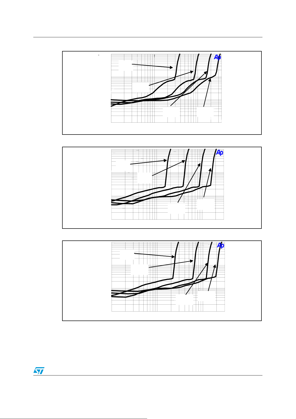
2.2.1 THD versus output power
Figure 16. 4 Ohm (1/2)
1
5V
0.
0.1
0.0
0.02
0.01
100
200
8V
500m12
Vcc=18 V
12V
16V
12/42
Page 13
AN2479 Test curve report
0
2
5
20.51 2 5
%
m30
m
m12
51020
W
0
2
5
20.51 2 5
%
m
m
2
51020
W
0
0
2
5
20.51 2 5
%
m30
m
m12
51020
W
Figure 17. 4 Ohm (2/2)
1
6V
10V
0.
0.1
0.0
0.0
0.01
100
14V
500
18V
200
Figure 18. 6 Ohm (1/2)
1
5V
0.
0.1
0.0
0.0
0.01
100m200
Figure 19. 6 Ohm (2/2)
1
0.
0.1
0.0
0.0
0.01
100
6V
200
500
10V
8V
500
12V
1
14V
16V
18V
3
13/42
Page 14

Test curve report AN2479
0
2
5
20.51 2 5
%
m30
m
m12
51020
W
0
2
5
20.51 2 5 %
m30
m
m12
51020
W
A
Figure 20. 8 Ohm (1/2)
1
5V
0.
0.1
0.0
0.0
0.01
100
Figure 21. 8 Ohm (2/2)
1
0.
0.1
0.0
0.0
0.01
100
200
6V
200
8V
500
10V
500
12V
14V
16V
18V
2.3 FFT
Figure 22. 0 dBFS@ 1 KHz 5 V 4 ohm
+10
+0
-10
-20
-30
-40
-50
d
-60
B
-70
r
-80
-90
-10 0
-11 0
-12 0
-13 0
-14 0
-15 0
20 20k50 100 200 500 1k 2k 5k 10k
14/42
Page 15

AN2479 Test curve report
A
10
A
A
Figure 23. -60 dBFS@ 1 KHz 5 V 4 ohm
+10
+0
-10
-20
-30
-40
-50
d
-60
B
-70
r
-80
-90
-100
-110
-120
-130
-140
-150
20 20k50 100 200 500 1k 2k 5k 10k
Figure 24. 0 dBFS@ 1 KHz 5 V 6 ohm
+
+0
-10
-20
-30
-40
-50
d
-60
B
-70
r
-80
-90
-100
-110
-120
-130
-140
-150
20 20k50 100 200 500 1k 2k 5k 10k
Figure 25. -60 dBFS@ 1 KHz 5 V 6 ohm
+10
+0
-10
-20
-30
-40
-50
d
-60
B
-70
r
-80
-90
-100
-110
-120
-130
-140
-150
20 20k50 100 200 500 1k 2k 5k 10k
15/42
Page 16

Test curve report AN2479
A
A
Figure 26. 0 dBFS@ 1 KHz 5 V 8 ohm
+10
+0
-10
-20
-30
-40
-50
d
-60
B
-70
r
-80
-90
-100
-110
-120
-130
-140
-150
20 20k50 100 200 500 1k 2k 5k 10k
Figure 27. -60 dBFS@ 1 KHz 5 V 8 ohm
+10
+0
-10
-20
-30
-40
-50
d
-60
B
-70
r
-80
-90
-100
-110
-120
-130
-140
-150
20 20k50 100 200 500 1k 2k 5k 10k
16/42
Page 17

AN2479 Test curve report
A
10
A
Figure 28. 0 dBFS@ 1 KHz 12 V 4 ohm
+10
+0
-10
-20
-30
-40
-50
d
-60
B
-70
r
-80
-90
-100
-110
-120
-130
-140
-15 0
20
Hz
20k50 100 200 500 1k 2k 5k 10k
Figure 29. -60 dBFS@ 1 KHz 12 V 4 ohm
+
+0
-10
-20
-30
-40
-50
-60
d
B
-70
r
-80
-90
-100
-110
-120
-130
-140
-150
20
20k50 100 200 500 1k 2k 5k 10k
17/42
Page 18

Test curve report AN2479
A
A
Figure 30. 0 dBFS@ 1 KHz 12 V 6 ohm
+10
+0
-10
-20
-30
-40
-50
d
-60
B
-70
r
-80
-90
-10 0
-11 0
-12 0
-13 0
-14 0
-15 0
20 50 1 00 200 500 1k 2k 5k 10k
Hz
20k
Figure 31. -60 dBFS@ 1 KHz 12 V 6 ohm
+10
+0
-10
-20
-30
-40
-50
-60
d
B
-70
r
-80
-90
-100
-110
-120
-130
-140
-15 0
20
Hz
20k50 100 200 500 1k 2k 5k 10k
18/42
Page 19

AN2479 Test curve report
A
10
A
Figure 32. 0 dBFS@ 1 KHz 12 V 8 ohm
+10
+0
-10
-20
-30
-40
-50
-60
d
B
-70
r
-80
-90
-100
-110
-120
-130
-140
-150
20 20k50 100 200 500 1k 2k 5k 10k
Hz
Figure 33. -60 dBFS@ 1 KHz 12 V 8 ohm
+
+0
-10
-20
-30
-40
-50
d
-60
B
-70
r
-80
-90
-100
-110
-120
-130
-140
-150
20
Hz
20k50 100 200 500 1k 2k 5k 10k
19/42
Page 20

Test curve report AN2479
A
10
A
Figure 34. 0 dBFS@ 1 KHz 18 V 4 ohm
+10
+0
-10
-20
-30
-40
-50
-60
d
B
-70
r
-80
-90
-100
-
110
-120
-130
-140
-150
20
Hz
20k50 100 200 500 1k 2k 5k 10k
Figure 35. -60 dBFS@ 1 KHz 18 V 4 ohm
+
+0
-10
-20
-30
-40
-50
d
-60
B
-70
r
-80
-90
-100
-110
-120
-130
-140
-150
20
Hz
20k50 100 200 500 1k 2k 5k 10k
20/42
Page 21

AN2479 Test curve report
A
A
Figure 36. 0 dBFS@ 1 KHz 18 V 6 ohm
+10
+0
-10
-20
-30
-40
-50
d
-60
B
-70
r
-80
-90
-100
-110
-120
-130
-140
-150
20
Hz
20k50 100 200 500 1k 2k 5k 10k
Figure 37. -60 dBFS@ 1 KHz 18 V 6 ohm
+10
+0
-10
-20
-30
-40
-50
d
-60
B
-70
r
-80
-90
-100
-110
-120
-130
-140
-150
20
Hz
20k50 100 200 500 1k 2k 5k 10k
21/42
Page 22

Test curve report AN2479
A
A
Figure 38. 0 dBFS@ 1 KHz 18 V 8 ohm
+10
+0
-10
-20
-30
-40
-50
d
-60
B
-70
r
-80
-90
-100
-110
-120
-130
-140
-150
20
Hz
20k50 100 200 500 1k 2k 5k 10k
Figure 39. -60 dBFS@ 1 KHz 18 V 8 ohm
+10
+0
-10
-20
-30
-40
-50
d
-60
B
-70
r
-80
-90
-100
-110
-120
-130
-140
-150
20
Hz
20k50 100 200 500 1k 2k 5k 10k
22/42
Page 23

AN2479 Test curve report
r
A
k
k5k10k
r
A
k
k
k
2.4 Cross talk
Figure 40. 5 V 4 ohm 1 W @ 1 KHz
+0
-10
-20
-30
-40
d
B
-50
-60
-70
-80
-90
-100
20 20
50 100 200 500 1k2
Figure 41. 12 V 4 ohm 1 W @ 1 KHz
Hz
d
B
-100
+0
-10
-20
-30
-40
-50
-60
-70
-80
-90
20
50 100 200 500 1k2
Hz
5k 10
20
23/42
Page 24

Test curve report AN2479
A
k
r
A
k
k5k
Figure 42. 18 V 4 ohm 1 W @ 1 KHz
+0
-10
-20
-30
-40
d
B
-50
r
-60
-70
-80
-90
-100
20
50 100 200 500 1k 2k 5k 10k
Hz
20
Figure 43. 5 V 6 ohm 1 W @ 1 KHz
+0
-10
-20
-30
-40
d
B
-50
-60
-70
-80
-90
-100
20
50 100 200 500 1k 2
Hz
10k
20
24/42
Page 25

AN2479 Test curve report
r
A
k
k5k
r
A
k
k5k
Figure 44. 12 V 6 ohm 1 W @ 1 KHz
+0
-10
-20
-30
-40
d
B
-50
-60
-70
-80
-90
-100
20
50 100 200 500 1k 2
Hz
10k
20
Figure 45. 18 V 6 ohm 1 W @ 1 KHz
+0
-10
-20
-30
-40
d
B
-50
-60
-70
-80
-90
-100
20
50 100 200 500 1k 2
Hz
10k
20
25/42
Page 26

Test curve report AN2479
r
A
k
k5k
r
A
k
k5k
Figure 46. 5 V 8 ohm 1 W @ 1 KHz
+0
-10
-20
-30
-40
d
B
-50
-60
-70
-80
-90
-100
20
50 100 200 500 1k 2
Hz
10k
20
Figure 47. 12 V 8 ohm 1 W @ 1 KHz
+0
-10
-20
-30
-40
d
B
-50
-60
-70
-80
-90
-100
20
50 100 200 500 1k 2
Hz
10k
20
26/42
Page 27

AN2479 Test curve report
r
A
k
k5k
Figure 48. 18 V 8 ohm 1 W @ 1 KHz
+0
-10
-20
-30
-40
d
B
-50
-60
-70
-80
-90
-100
20
50 100 200 500 1k 2
Hz
10k
20
27/42
Page 28

Design guideline for PCB schematic and layout AN2479
3 Design guideline for PCB schematic and layout
3.1 Schematic
3.1.1 Main driver for components selection
● Absolute maximum rate: 20 V.
● Bypass capacitor 100 nF in parallel to 1 µF for each power Vcc branch. Preferable
dielectric is X7R.
● Vdd and ground for PLL filter separate of the power supply.
● Coil saturation current compatible with the peak current of the application.
3.2 Decoupling capacitors
There are two different ways to use the decoupling capacitors:
● shared among the channels: the best practise layout route must be used for the board,
● one decoupling system per channel: it is mandatory that the decoupling capacitor must
be as close as possible to the IC pins.
3.2.1 Output filter
Figure 49. Output filter
INxA
INxB
● The key function of a snubber network is to absorb energy from the reactance in the
power circuit. The purpose of the snubber RC network is in order to avoid the high
pulse energy (such as spikes) in the power circuit which can be dangerous to the
system. When using the snubber network, the energy is be transferred to and from the
snubber network, ensuring the system can work safely.
L11
C90
330p
R36
20
L13 22u
22u
C89
100n
C95
100n
C101
100n
C105
100n
R34
6.2
R37
6.2
C98
470n
Damping networkMain filterSnubber
C91
1000p
C103
1000p
C99
1000p
J7
1
2
CON2
28/42
Page 29

AN2479 Design guideline for PCB schematic and layout
● The purpose of the main filter is to remove frequency higher than audible range of
20 KHz. The main filter uses the Butterworth formula to define the cut off frequency,
which must be higher than 20 KHz, otherwise the frequency response is affected.
● The purpose of the damping network is to avoid high frequency oscillation on the output
circuit. After using the damping network the THD can be improved, and can also avoid
the inductive copper on the PCB route when the system is working in high frequency
with PWM or PCM.
Snubber filter
The snubber circuit must be optimized for the application. Starting values are 330 pF in
series to 22 ohm. The power can be defined by the following formula which considers the
power supply, frequency and capacitor value:
P=C*f*(2*V)^2
This power is dissipated in series resistance.
Figure 50. Snubber filter
INxA
C126
330p
R44
22
INxB
Damping network
The C-R-C is a damping network. It is mainly intended for high inductive loads.
Figure 51. Damping filter
C du mp - S
C du mp - P
C du mp - P
C du mp - S
R dump
Rdump
Main filter
The main filter is an L and C based Butterworth filter. The cut-off frequency must be chosen
between the upper limit of the audio band (20 KHz) and the carrier frequency (384 KHz).
29/42
Page 30

Design guideline for PCB schematic and layout AN2479
d
Figure 52. Main filter
C
load
-----------------------------------------------------------------=
22 Π f
L
load
---------------------------------------------------=
2 Π 2× f
F
cutoff
---------------------------------------------------------------------- -=
2 Π× 2C
Recommended values
Rload
Lload
Cload
C dump-S
C dump-P
R dump
8 ohm 4 ohm
22 µH10µH
470 nF 1 µH
100 nF 220 nF
220 nF 220 nF
6.2 2.7
1
cutoff
1
R
load
load
×××
××
×××
R
load
cutoff
L
load
Lload
INxA
C load
Rlo a
INxB
Lload
Recommended power up and power down sequence
Figure 53. Main filter
Vcc
5 V
0V
Vlogic
0V
Reset
0V
Play
30/42
Page 31

AN2479 Design guideline for PCB schematic and layout
3.3 Layout
1. Solder snubber network as close as possible to the IC related pin.
Figure 54. Snubber network
Snubber network
2. Use electrolytic capacitor first to separate the Vcc branches.
Figure 55. Separate the Vcc branches
Separate from the E-cap
3. Minimize the path between Vcc pins and ground pin in order to avoid inductive paths.
Figure 56. Minimized paths between Vcc and GND
GND
Vcc
4. To dissipate the thermal with a ground plane.
31/42
Page 32

Design guideline for PCB schematic and layout AN2479
Figure 57. Dissipate thermal
GND
Big ground plane
5. Solder PLL filter as close as possible to the FILT pin.
Figure 58. PLL filter
6. For differential application create symmetrical paths for the output stage.
PLL filter
32/42
Page 33

AN2479 Design guideline for PCB schematic and layout
Figure 59. Dissipate thermal
Symmetrical
output paths
7. Separate the coil and the neighboring coil are vertical to avoid crosstalk.
33/42
Page 34

Design guideline for PCB schematic and layout AN2479
Figure 60. Avoiding crosstalk
Ver t ical
Ver t ical
8. It is better to use a polyester filter capacitor.
Figure 61. Filter capacitor
Separate the coils to avoid
crosstalk
Filter capacitors should be metal or polyester
9. Consider ground layout. To avoid interference between ground power and small signal
ground, it is necessary to divide the grounding as shown in Figure 62.
34/42
Page 35

AN2479 Design guideline for PCB schematic and layout
Figure 62. Ground layout
Channel ground plane
Power ground plane
10. Thermal layout with large ground (1 of 2 for top and bottom layers).
Figure 63. Thermal layout (1 of 2)
Thermal layout on
the top layer
Thermal layout on
the bottom layer
11. Thermal layout with big ground (2 of 2 for thermal and soldering holes).
The thermal resistance junction at the bottom of the STA333ML to the ambient
obtainable with a ground copper area of 4 x 4 cm and with 35 via holes (see Figure 64).
Figure 64. Thermal layout (2 of 2)
35 via holes ϕ:1.0 mm
12. VCC routing.
The best route for the Vcc supply is one which avoids interference between different
signals (for example, part A is idle whilst part B is working at full load).
35/42
Page 36

Design guideline for PCB schematic and layout AN2479
Figure 65. Vcc routing
Best method to isolate the two channels
amplifiers are isolated from each other
Good Vcc routing
13. Vcc filter for high frequency.
The PWM system works with a fast switch (frequency of 340 KHz approximately) which
means the copper wire works as a coil. In order to avoid this, a ceramic capacitor
should be used to balance resistance. It is a mandatory requirement that ceramic
capacitors are placed as close as possible to the related pins. The distance between
the capacitor and their respective pins should be less then 5 mm in order to minimize
inductive coil effect generated by the copper wire.
36/42
two amplifiers are daisy chained
Bad Vcc routing
Page 37

AN2479 Design guideline for PCB schematic and layout
Figure 66. Vcc filter
Vcc capacitor filter as close to the related pins as
possible. The ceramic capacitors on the bottom
of the PCB close to the IC due to SMD mounting
limitations.
14. Decoupling capacitors.
Solder decoupling capacitors as close as possible to their respective IC pin. This
reduces the inductive coil effect.
Figure 67. Decoupling capacitors
Good amplifier bypassing
capacitors are properly placed
Bad amplifier bypassing, capacitors are
out of order and ground connection is indirect
15. Snubber filters for high frequency spike protection on the PWM.
37/42
Page 38

Design guideline for PCB schematic and layout AN2479
Figure 68. Snubber filter placement
Place snubber circuit as close
as possible to the appropriate
IC pins, and the - and + for
each channel.
Figure 69. Examples of snubber filter placement
Good common mode snubber placement
Good differential snubber placement
Caution: A spike can occur if there > 3 mm distance between the snubber network and the pins. This
can cause damage to the IC. Therefore the distance must be kept below 3 mm.
16. Output routing
38/42
Page 39

AN2479 Design guideline for PCB schematic and layout
Figure 70. Output routing
Good output routing
traces grow wider as space allows
Good output routing
area between outputs is small
Bad output routing
area between outputs is large
17. Thermal layout
Note: The thermal pad must be connected to ground in order to properly set the IC references. It is
necessary to allow the heat to flow freely to all sides of the board including top and bottom.
For optimum heat dissipation it is recommended that the PCB has some solder via holes.
39/42
Page 40

Design guideline for PCB schematic and layout AN2479
Figure 71. Output routing
Good thermal layout (top)
heat can flow freely to the sides
Good thermal layout (bottom)
plenty of copper area
Bad thermal layout (top)
heat flow cut off by the snubbers
Bad output routing (bottom)
little copper area on 3 sides
40/42
Page 41

AN2479 Revision history
4 Revision history
Table 2. Document revision history
Date Revision Changes
06-Dec-2006 1 Initial release.
41/42
Page 42

AN2479
Please Read Carefully:
Information in this document is provided solely in connection with ST products. STMicroelectronics NV and its subsidiaries (“ST”) reserve the
right to make changes, corrections, modifications or improvements, to this document, and the products and services described herein at any
time, without notice.
All ST products are sold pursuant to ST’s terms and conditions of sale.
Purchasers are solely responsible for the choice, selection and use of the ST products and services described herein, and ST assumes no
liability whatsoever relating to the choice, selection or use of the ST products and services described herein.
No license, express or implied, by estoppel or otherwise, to any intellectual property rights is granted under this document. If any part of this
document refers to any third party products or services it shall not be deemed a license grant by ST for the use of such third party products
or services, or any intellectual property contained therein or considered as a warranty covering the use in any manner whatsoever of such
third party products or services or any intellectual property contained therein.
UNLESS OTHERWISE SET FORTH IN ST’S TERMS AND CONDITIONS OF SALE ST DISCLAIMS ANY EXPRESS OR IMPLIED
WARRANTY WITH RESPECT TO THE USE AND/OR SALE OF ST PRODUCTS INCLUDING WITHOUT LIMITATION IMPLIED
WARRANTIES OF MERCHANTABILITY, FITNESS FOR A PARTICULAR PURPOSE (AND THEIR EQUIVALENTS UNDER THE LAWS
OF ANY JURISDICTION), OR INFRINGEMENT OF ANY PATENT, COPYRIGHT OR OTHER INTELLECTUAL PROPERTY RIGHT.
UNLESS EXPRESSLY APPROVED IN WRITING BY AN AUTHORIZED ST REPRESENTATIVE, ST PRODUCTS ARE NOT
RECOMMENDED, AUTHORIZED OR WARRANTED FOR USE IN MILITARY, AIR CRAFT, SPACE, LIFE SAVING, OR LIFE SUSTAINING
APPLICATIONS, NOR IN PRODUCTS OR SYSTEMS WHERE FAILURE OR MALFUNCTION MAY RESULT IN PERSONAL INJURY,
DEATH, OR SEVERE PROPERTY OR ENVIRONMENTAL DAMAGE. ST PRODUCTS WHICH ARE NOT SPECIFIED AS "AUTOMOTIVE
GRADE" MAY ONLY BE USED IN AUTOMOTIVE APPLICATIONS AT USER’S OWN RISK.
Resale of ST products with provisions different from the statements and/or technical features set forth in this document shall immediately void
any warranty granted by ST for the ST product or service described herein and shall not create or extend in any manner whatsoever, any
liability of ST.
ST and the ST logo are trademarks or registered trademarks of ST in various countries.
Information in this document supersedes and replaces all information previously supplied.
The ST logo is a registered trademark of STMicroelectronics. All other names are the property of their respective owners.
© 2006 STMicroelectronics - All rights reserved
STMicroelectronics group of companies
Australia - Belgium - Brazil - Canada - China - Czech Republic - Finland - France - Germany - Hong Kong - India - Israel - Italy - Japan -
Malaysia - Malta - Morocco - Singapore - Spain - Sweden - Switzerland - United Kingdom - United States of America
www.st.com
42/42
 Loading...