

Page 1

AN2474
Application note
TS4995 1.2W fully differential audio power amplifier with selectable
standby and 6db fixed gain - Evaluation board user guidelines
Introduction
This application note describes the DEMO TS4995, an evaluation board specifically
designed for the TS4995 differential audio amplifier. In this document, you will find:
● a brief description of the TS4995 differential audio amplifier ,
● a description of the evaluation board,
● a detailed list of evaluation board components,
● the layout of the evaluation board.
About the TS4995
The TS4995 is fully differential structure po wer audio amplifier which is capab le of deliv ering
1.2W of continuous RMS output power into an 8Ω load at 5V. Due to its differential inputs, it
exhibits outstanding noise immunity.
An external standby mode control reduces the supply curre nt to less than 10nA. A STBY
MODE pin allows the standby to be acti ve High or Low. An internal thermal shutdown
protection is also provided, making the device capable of su staining short-circuits.
The TS4995 features an internal fixed gain at 6dB which reduces the number of external
components on the application board, and the flip-chip package with 9 bumps allows
maximum space saving.
Its key features are:
● Differential inputs
● 90dB PSRR @ 217Hz with grounded inputs
● Operating range from V
● 1.2W rail to rail output power @ V
● 6dB integrated fixed gain
● Ultra-low consumption in standby mode (10nA)
● Selectable standby mode (active low or active high)
● Ultra-fast startup time: 10ms typ. at V
● Available in 9-bump flip-chip (300mm bump diameter)
● Ultra-low pop & click
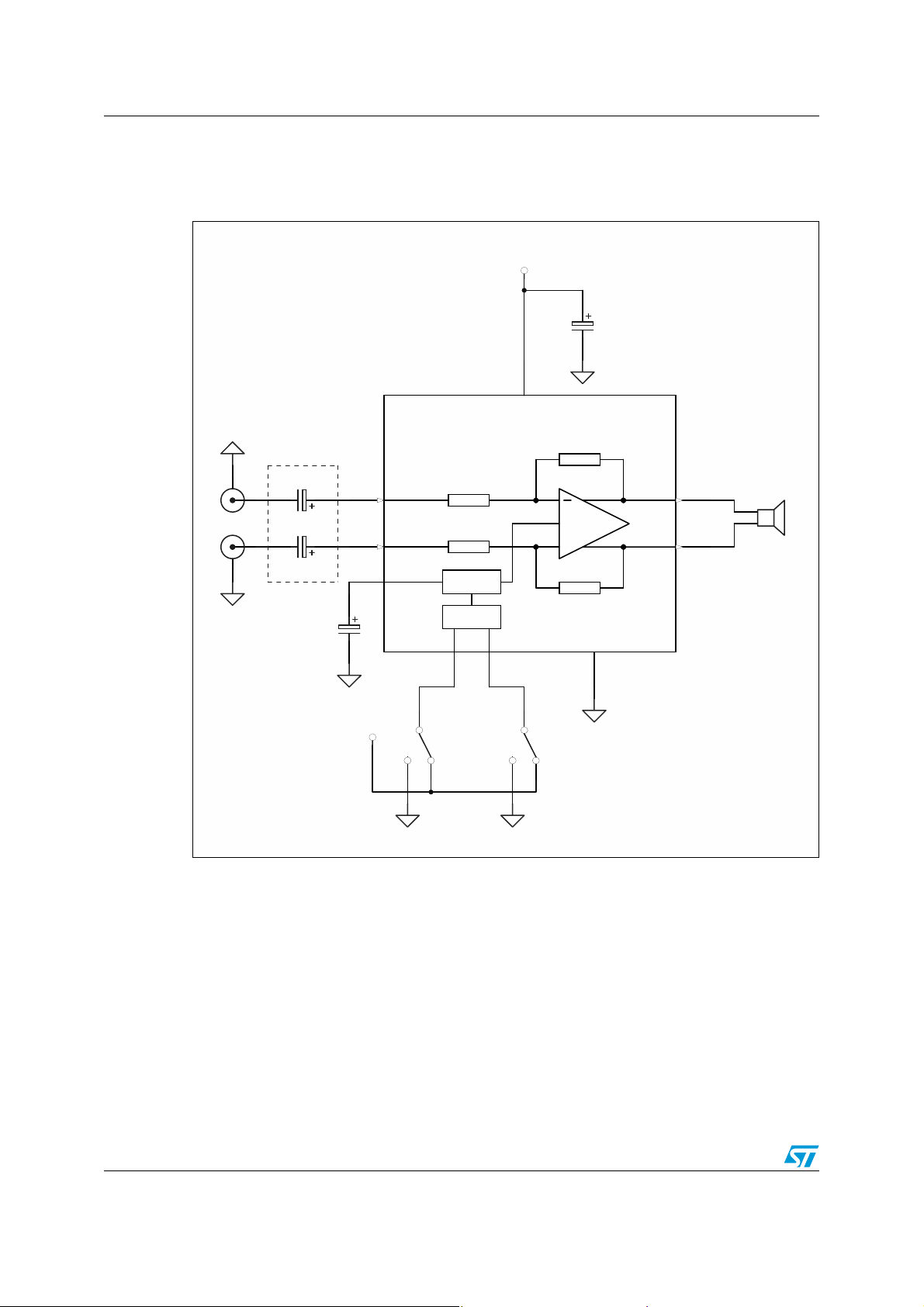
Figure 1 on page 2 shows a typical application for the TS4995 amplifier.
For more detailed information about the TS4995, refer to the datasheet.
= 2.5V to 5.5V
CC
CC
=5V, THD+N=1%, F=1kHz, with 8Ω load
=3.3V
CC
January 2007 Rev 1 1/7
www.st.com
Page 2
Typical application AN2474
1 Typical application
Figure 1. Typical application for the TS4995 audio amplifier
VCC
Cs1
1uF
VinP1
P2
Vin+
Optional
Cin1
330nF
Cin2
330nF
Cbypass1
1uF
3
1
8
VCC
TS4995
Vin-
Vin+
BYPASS
STDBY
2
3
2
Vcc
TS4995 FlipChip
+
Vo-
Vo+
7
5
8 Ohms
BIAS
STBY
STDBY MO DE
4
9
2
1
STD BY / Ope ration
1
3
GND
6
STDBY MODE
2/7
Page 3
AN2474 Description of the evaluation board
2 Description of the evaluation board
The DEMO TS4995 is an evaluation board designed to help you evaluate the TS4995 low
power differential audio amplifier.
This section explains how to evaluate the amplifier in a ty pical application configuration.
Using the board, you can:
● set the amplifier in standby/operat ion mode,
● select standby mode (active low or active high),
● modify the input configuration from capacitor coupled to common mode feedback.
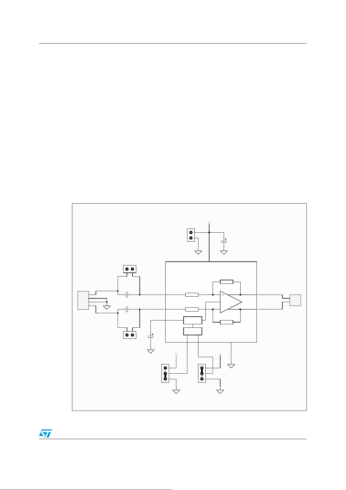
The Cn4 connector is used to select between standby or operation mode; and the Cn5
connector is used for standby to select between active low or active high. For example, in
Figure 2, the jumper that connects pin 2 and pin 3 of the Cn4 connector puts the device in
standby mode, while the jumper t hat connects pin1 and pin 2 of the Cn5 connector
determines that the standby is active high.
When the amplifier is used in common mode feedback input configuration, the input
capacitors are shorted by placing jumpers on connectors Cn2 and Cn3.
Figure 2. Evaluation board schematic diagram
JP1
VCC
Cn1
12
Cs
1uF
STBY MODE
8
Cn5
1
2
3
4
Vcc
Vo-
13
Vo+
+
GND
11
9
JP2
1
2
Cn2
Cin1
4
3
2
1
1 2
330nF
Cin2
1 2
330nF
Cn3
U1
TS4995
5
Vin-
3
Vin+
2
BYPASS
12
Cb
1uF
Cn4
1
2
3
BIAS
STBY
STBY
6
VCC VCC
3/7
Page 4

Description of the evaluation board AN2474
Table 1. Evaluation board bill of materials
Designation Quantity Description
U1 1
DIP14 socket with plugged flipchip to DIP adapter with the
TS4995 audio amplifier
C1, C2 2 330nF/63V, ceramic capacitors
Cb, Cs 2 1μF/50V, electrolytic capa citor
--- 2 Jumper, 2.54mm pitch (placed on Cn4 and Cn5 connectors)
Cn1, Cn2, Cn3 1 2 pins header, 2.54mm pitch
Cn4, Cn5 2 3 pins header, 2.54mm pitch
JP1 1 4 pins header, 2.54mm pitch
JP2 1 2 pins header, 2.54mm pitch
Figure 3. TS4995 flip-chip adapter
4/7
Page 5

AN2474 Evaluation board connectors
3 Evaluation board connectors
Connector(s) Description
Cn1 Power connector (V
Cn2
Cn3
Connector used to short-circuit input capacitor C
the amplifier is used with common mode feedback in put.
Connector used to short-circuit input capacitor C
the amplifier is used with common mode feedback in put.
Cn4 Standby control connector (GND, Standby, V
Cn5
Standby mode control connector (V
standby mode active high or low .
JP1 Input signal connector (V
, GND). Power supply voltage from 2.5V to 5.5V.
CC
1 by placing jumper on it when
in
2 by placing jumper on it when
in
).
CC
, Standby, GND). Allows you to select
CC
, V
, 2 x GND).
in-
in+
JP2 Output signal connector (Vo-, Vo+).
Caution: When yo u apply the po wer supply th rough Cn1, DO N O T inv ert the polarity because it would
destroy the amplifier at U1.
5/7
Page 6

Evaluation board layout AN2474
4 Evaluation board layout
The following schematics show the layers and the top view of the evaluation board.
Figure 4. PCB top layer Figure 5. PCB bottom layer
Figure 6. Top view of evaluation board
6/7
Page 7

AN2474
Please Read Carefully:
Information in this document is provided solely in connection with ST products. STMicroelectronics NV and its subsidiaries (“ST”) reserve the
right to make changes, corrections, modifications or improvements, to this document, and the products and services described herein at any
time, without notice.
All ST products are sold pursuant to ST’s terms and conditions of sale.
Purchasers are solely res ponsibl e fo r the c hoic e, se lecti on an d use o f the S T prod ucts and s ervi ces d escr ibed he rein , and ST as sumes no
liability whatsoever relati ng to the choice, selection or use of the ST products and services described herein.
No license, express or implied, by estoppel or otherwise, to any intellectual property rights is granted under this document. If any part of this
document refers to any third pa rty p ro duc ts or se rv ices it sh all n ot be deem ed a lice ns e gr ant by ST fo r t he use of su ch thi r d party products
or services, or any intellectua l property c ontained the rein or consi dered as a warr anty coverin g the use in any manner whats oever of suc h
third party products or servi ces or any intellectual property contained therein.
UNLESS OTHERWISE SET FORTH IN ST’S TERMS AND CONDITIONS OF SALE ST DISCLAIMS ANY EXPRESS OR IMPLIED
WARRANTY WITH RESPECT TO THE USE AND/OR SALE OF ST PRODUCTS INCLUDING WITHOUT LIMITATION IMPLIED
WARRANTIES OF MERCHANTABILITY, FITNESS FOR A PARTICUL AR PURPOS E (AND THEIR EQUIVALE NTS UNDER THE LAWS
OF ANY JURISDICTION), OR INFRINGEMENT OF ANY PATENT, COPYRIGHT OR OTHER INTELLECTUAL PROPERTY RIGHT.
UNLESS EXPRESSLY APPROVED IN WRITING BY AN AUTHORIZED ST REPRESENTATIVE, ST PRODUCTS ARE NOT
RECOMMENDED, AUTHORIZED OR WARRANTED FOR USE IN MILITARY, AIR CRAFT, SPACE, LIFE SAVING, OR LIFE SUSTAINING
APPLICATIONS, NOR IN PRODUCTS OR SYSTEMS WHERE FAILURE OR MALFUNCTION MAY RESULT IN PERSONAL INJ URY,
DEATH, OR SEVERE PROPERTY OR ENVIRONMENTAL DAMAGE. ST PRODUCTS WHICH ARE NOT SPECIFIED AS "AUTOMOTIVE
GRADE" MAY ONLY BE USED IN AUTOMOTIVE APPLICATIONS AT USER’S OWN RISK.
Resale of ST products with provisions different from the statements and/or technical features set forth in this document shall immediately void
any warranty granted by ST fo r the ST pro duct or serv ice describe d herein and shall not cr eate or exten d in any manne r whatsoever , any
liability of ST.
ST and the ST logo are trademarks or registered trademarks of ST in various countries.
Information in this document su persedes and replaces all information previously supplied.
The ST logo is a registered trademark of STMicroelectronics. All other names are the property of their respective owners.
© 2007 STMicroelectronics - All rights reserved
STMicroelectronics group of compan ie s
Australia - Belgium - Brazil - Canada - China - Czech Republic - Finland - France - Germany - Hong Kong - India - Israel - Italy - Japan -
Malaysia - Malta - Morocco - Singapore - Spain - Sweden - Switzerland - United Kingdom - United States of America
www.st.com
7/7
 Loading...