

Page 1
AN2471
Application note
STMAV335 evaluation board &
PCB layout recommendation
Introduction
STMAV335 has three sets of 3 to 1 switches that are well suited for switching analog video
signals on the back panel of television sets or monitors. Below is a diagram of an
STMAV335 typical application configuration:
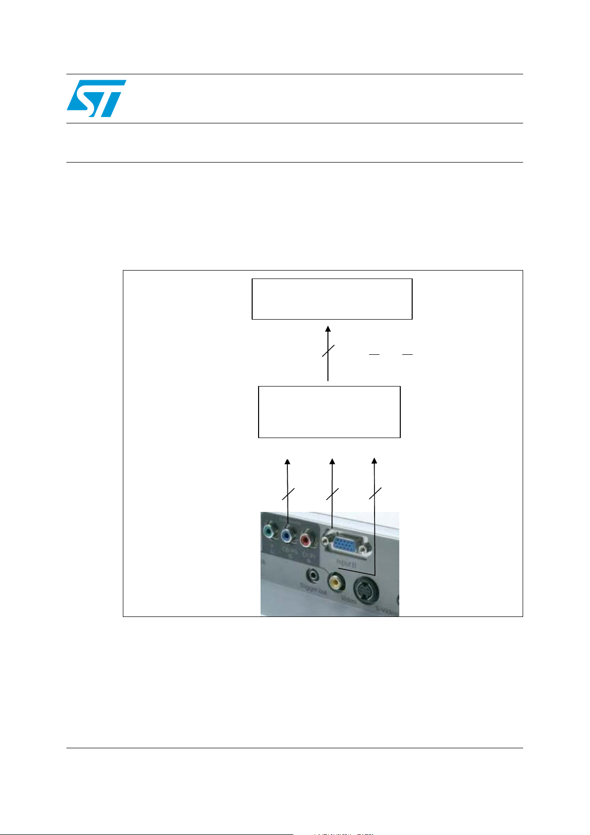
Typical display unit back panel video input
VIDEO RECEIVER
YPbPr OR R G B OR C V BS & S-V ID E O
STM A V335
YPbPr
As illustrated above, STMAV335 is used to switch one of the three video input sets to the
video receiver. Depending on the SEL inputs, YPbPr, RGB, or CVBS&S-VIDEO signals will
be directed to the video receiver. Hence less IO is required at the video receiver to handle
the many different video signal inputs on the display unit back panel.
Ultimately, integrating STMAV335 to the system will result in a straightforward system
design and overall cost reduction.
RGB
-
March 2007 Rev 1 1/12
www.st.com
Page 2

Contents AN2471
Contents
1 Evaluation board . . . . . . . . . . . . . . . . . . . . . . . . . . . . . . . . . . . . . . . . . . . . 3
1.1 Power supply . . . . . . . . . . . . . . . . . . . . . . . . . . . . . . . . . . . . . . . . . . . . . . . 3
2 Video input & output ports . . . . . . . . . . . . . . . . . . . . . . . . . . . . . . . . . . . . 4
2.1 Video input conditioning . . . . . . . . . . . . . . . . . . . . . . . . . . . . . . . . . . . . . . . 4
3 PCB layout recommendation . . . . . . . . . . . . . . . . . . . . . . . . . . . . . . . . . . 7
4 Revision history . . . . . . . . . . . . . . . . . . . . . . . . . . . . . . . . . . . . . . . . . . . 11
2/12
Page 3
AN2471 Evaluation board
1 Evaluation board
The STMAV335 evaluation board provides the customer with straightforward evaluation on
the performance and the typical use of the switch in the real system.
The boards include an STMAV335 switch, video input and output connectors, jumper for
setting the control lines status, and a power supply portion.
1.1 Power supply
The board can be powered either directly from a DC power supply or from a DC adaptor. If it
is powered from a DC power supply, 5VDC is connected to the power socket labeled
VCC5V and the ground is connected to the power socket labeled GND. The board can also
be powered from a DC adaptor having output voltage of 7 V to 15 V. The DC adaptor voltage
will be regulated to 5 V by the on-board regulator. The DC adaptor can be center positive or
negative and it should be connected to the DC JACK.
To prevent digital noise from coupling to the analog lines, the power distribution is separated
from digital and analog sections. Though STMAV335 has also two digital lines, which are
SEL1 and SEL2, it should still be powered from the analog supply. The reason is because its
main function is to switch analog signals and those two digital lines are mostly static during
operation. Hence the analog lines will not be disturbed by the digital part and as such, there
is no need to have a separate analog and digital supply for STMAV335.
The analog and digital sections on the board are isolated by ferrite beads.
Table 1. Power connector
Designator Notes
VCC5V Connect to 5 V of external power supply.
GND Connect to ground of external power supply.
Connect to DC adaptor output if the board is to be
DC JACK
Note: External power can be applied to either VCC5V/GND or DC JACK, but not to both.
powered from DC adaptor.
Input Voltage: 7 to 15 V
3/12
Page 4
Video input & output ports AN2471
2 Video input & output ports
STMAV335 can switch three sets of video input to a single set of video output. On the
evaluation board, the three sets of video input are:
1. RGB (VGA port)
2. YPbPr (3 RCA connector)
3. CVBS (RCA connector) & S-VIDEO ( S-connector)
In the real system, the outputs of STMAV335 are directly connected to the video receiver.
However for the STMAV335 evaluation board, each output line branches to three signal
lines. The reason for this is because each set of different video signal has a different type of
connector. During evaluation, each output line should be branched and be connected to a
different video connector on the display unit back panel by a cable.
To avoid any PCB trace stub, the 1 to 3 branching of each output line cannot be shorted on
the board. The branching of the output line is done by a zero ohm resistor. Depending on
which particular set of video signal is active, the zero ohm resistors should be soldered such
that the output of STMAV335 is connected to the right video output connector.
Table 2. Evaluation board video input & output
Input Output SEL 0Ω Jumper output
RGB (VGA_IN) RGB (VGA_OUT)
Y (Y_IN)
Pb (Pb_IN)
Pr (Pr_IN)
CVBS (CVBS_IN)
S-VIDEO
(S VIDEO_IN)
Y (Y_OUT)
Pb (Pb_OUT)
Pr (Pr_OUT)
CVBS (CVBS_OUT)
S-VIDEO
(S VIDEO_OUT)
SEL1 = ‘1’
SEL2 = ‘0’
SEL1 = ‘0’
SEL2 = ‘1’
SEL1 = ‘0’
SEL2 = ‘0’
Note: SEL1→ JP9, SEL2 → JP10, OPEN = '1' & CLOSE = '0'
2.1 Video input conditioning
The blanking level might vary between different video transmitters. This STMAV335
evaluation board can handle video signals with blanking level of 0V to 2.5 V.
If video signal blanking levels are outside the above range, some input conditioning should
be done to modify the blanking level to the range specified.
J11 = ‘R’
J12 = ‘G’
J13 = ‘B’
J11 = ‘Y’
J12 = ‘Pb’
J13 = ‘Pr’
J11 = ‘CVBS’
J12 = ‘Y(S)’
J13 = ‘C’
4/12
Page 5

AN2471 Video input & output ports
Figure 1. Board schematic
SHLD
5
Y_OUT
RCA
Pb_OUT
RCA
Pr_OUT
RCA
CVBS_OUT
RCA
AGND
CVBS_OUT
S VIDEO_OUT
Y GND1C GND2Y3C
AGND
Y(S)_OUT
4
C_OUT
RED_OUT1GREEN_OUT2BLUE_OUT3ID_24GND5RED_RTN6GREEN_RTN7BLUE_RTN8NC9SYNC_RTN10ID011ID112H_SYNC13V_SYNC14ID3
VGA_OUT
R_OUT
G_OUT
B_OUT
ID2
ID0
2
1
VGA_CON
15
ID1
H_SYNC
V_SYNC
ID3
AGND
Y_OUT
Pb_OUT
AGND
AGND
Pr_OUT
R_OUT
AGND
AGND
JP9
10K
R1
VCC5V_A
VCC5V_A
VCC5V
VCC5V
VCC5V_A
SEL1
100pF
C3
100nF
C2
10uF
C1
GND
JP10
10K
R2
VCC5V_A
SEL2
16
AGND
AGND
VCC
SEL11Y12Y23R4Pb15Pb26G7Pr/B
U1
SEL1
AGND
B
Pr
C
SEL2
CVBS/Y/R_OUT
Y(S)/Pb/G_OUT
12
11
9
13
14
15
B
Pr210Pr1
Y/R
Pb/G
GND
SEL2
8
R
G
Y
Pb
CVBS
Y(S)
C/Pr/B_OUT
Y_OUT
OUT12OUT23OUT3
JP11
1
CVBS/Y/R_OUT
STMAV335
G_OUT
CVBS_OUT
4
IN
Pb_OUT
OUT12OUT23OUT3
1 TO 3 JUMPER
JP12
1
Y(S)/Pb/G_OUT
L1
B_OUT
Y(S)_OUT
4
IN
Pr_OUT
C_OUT
4
OUT12OUT23OUT3
IN
1 TO 3 JUMPER
JP13
1 TO 3 JUMPER
1
C/Pr/B_OUT
AGND
L2
VCC5V VCC5V_A
Number RevisionSize
A
Title
VCC1GND2GND
DC JACK
4
+1-
U4
C4
3
VIN
VOUT
U5
2
VCC5V
Date: 4/17/2006 Sheet of
File: C:\Documents and Settings\..\STMAV335.SCHDOCDrawn By:
DC PLUG
3
~3~
BRIDGE RECT
2
10uF
GND
1
LD1117V50
VGA_IN
RGB
1
2
RED_IN
ID2
5
3
4
ID_2
GND
BLUE_IN
GREEN_IN
ID0
ID1
H_SYNC
V_SYNC
ID3
9
6
7
8
RED_RTN
BLUE_RTN
GREEN_RTN
14
10
12
15
NC
ID011ID1
ID3
H_SYNC13V_SYNC
SYNC_RTN
Y
2
Y_IN
VGA_CON
Pb
1
AGND
RCA
Pb_IN
Pr
AGND
RCA
Pr_IN
CVBS
AGND
RCA
AGND
CVBS_IN
RCA
Y(S)
C
3
4
1
2
C
Y
C GND
Y GND
SHLD
S VIDEO_IN
5
5/12
Page 6

Video input & output ports AN2471
Table 3. Bill of material
No Component Designator Package Manufacturer
1 STMAV335 U1 TSSOP16 STMicroelectronics
2 S-Video CON S VIDEO_IN, S VIDEO_OUT
3 VGA FEMALE CON VGA_IN, VGA_OUT
4 RCA CON
5 LD1117V50 U5 TO-220 STMicroelectronics
6 DF04M RECTIFIER U4 DFM GENERAL SEMI
7 DC JACK DC JACK
8 POWER SOCKET VCC5V, GND
8 POWER SOCKET VCC5V, GND
9 FERRITE BEAD L1, L2 1206
10 100 nF Cap C2,C3 0603
11 10 µF Electrolytic Cap C1, C4 Cap7.62 mm
12 Jumper JP9, JP10 HDR 2X1
13 10 kΩ Resistor R1, R2 0603
Y_IN, Pb_IN, Pr_IN,CVBS_IN, Y_OUT,
Pb_OUT, Pr_OUT, CVBS_OUT
14 0 Ω Resistor JP11, JP12, JP13 0603
6/12
Page 7

AN2471 PCB layout recommendation
3 PCB layout recommendation
For the purpose of maintaining 75 Ω track for all the analog lines, a 4-layer structure is
recommended. All the analog tracks are routed on the top and bottom layers of the board.
The middle two layers are used for both analog and digital ground.
The middle two layers are identical and separated into two sections, analog and digital
grounds. They are separated by a slot area and are only connected at the top layer through
ferrite bead. This ensures the digital noise will not get coupled to the analog portion.
All the analog tracks are referenced to the analog ground and all the digital tracks are
referenced to the digital ground. In this evaluation board SEL1&SEL2, that in the actual
system would come from the digital portion of the system, are included in the analog
portion. Since these two select digital lines will be mostly static during operation, it will not
cause any disruption to the analog portion.
STMAV335 supply is connected to VCC5V analog and GND analog. To further guarantee
the stability of STMAV335 supply, a 100 nF capacitor is used to decouple the VCC pin and
should be placed as close as possible to the pin. The stability of the analog supply lines is of
significant importance since the bias level of STMAV335 is referenced to it. Any instability on
the analog supply will affect the switch characteristics.
Each set of video signals, RGB, YPbPr, and YC (S-VIDEO) are routed with the same track
length. This will guarantee minimum channel-to-channel delay that will lead to minimum
display distortion.
Figure 2. Recommended board stack-up for 75 Ω impedance
7/12
Page 8

PCB layout recommendation AN2471
Figure 3. PCB top layer
8/12
Page 9

AN2471 PCB layout recommendation
Figure 4. PCB middle layer1&2
9/12
Page 10

PCB layout recommendation AN2471
Figure 5. PCB bottom layer
10/12
Page 11

AN2471 Revision history
4 Revision history
Table 4. Document revision history
Date Revision Changes
13-Mar-2007 1 Initial release
11/12
Page 12

AN2471
Please Read Carefully:
Information in this document is provided solely in connection with ST products. STMicroelectronics NV and its subsidiaries (“ST”) reserve the
right to make changes, corrections, modifications or improvements, to this document, and the products and services described herein at any
time, without notice.
All ST products are sold pursuant to ST’s terms and conditions of sale.
Purchasers are solely responsible for the choice, selection and use of the ST products and services described herein, and ST assumes no
liability whatsoever relating to the choice, selection or use of the ST products and services described herein.
No license, express or implied, by estoppel or otherwise, to any intellectual property rights is granted under this document. If any part of this
document refers to any third party products or services it shall not be deemed a license grant by ST for the use of such third party products
or services, or any intellectual property contained therein or considered as a warranty covering the use in any manner whatsoever of such
third party products or services or any intellectual property contained therein.
UNLESS OTHERWISE SET FORTH IN ST’S TERMS AND CONDITIONS OF SALE ST DISCLAIMS ANY EXPRESS OR IMPLIED
WARRANTY WITH RESPECT TO THE USE AND/OR SALE OF ST PRODUCTS INCLUDING WITHOUT LIMITATION IMPLIED
WARRANTIES OF MERCHANTABILITY, FITNESS FOR A PARTICULAR PURPOSE (AND THEIR EQUIVALENTS UNDER THE LAWS
OF ANY JURISDICTION), OR INFRINGEMENT OF ANY PATENT, COPYRIGHT OR OTHER INTELLECTUAL PROPERTY RIGHT.
UNLESS EXPRESSLY APPROVED IN WRITING BY AN AUTHORIZED ST REPRESENTATIVE, ST PRODUCTS ARE NOT
RECOMMENDED, AUTHORIZED OR WARRANTED FOR USE IN MILITARY, AIR CRAFT, SPACE, LIFE SAVING, OR LIFE SUSTAINING
APPLICATIONS, NOR IN PRODUCTS OR SYSTEMS WHERE FAILURE OR MALFUNCTION MAY RESULT IN PERSONAL INJURY,
DEATH, OR SEVERE PROPERTY OR ENVIRONMENTAL DAMAGE. ST PRODUCTS WHICH ARE NOT SPECIFIED AS "AUTOMOTIVE
GRADE" MAY ONLY BE USED IN AUTOMOTIVE APPLICATIONS AT USER’S OWN RISK.
Resale of ST products with provisions different from the statements and/or technical features set forth in this document shall immediately void
any warranty granted by ST for the ST product or service described herein and shall not create or extend in any manner whatsoever, any
liability of ST.
ST and the ST logo are trademarks or registered trademarks of ST in various countries.
Information in this document supersedes and replaces all information previously supplied.
The ST logo is a registered trademark of STMicroelectronics. All other names are the property of their respective owners.
© 2007 STMicroelectronics - All rights reserved
STMicroelectronics group of companies
Australia - Belgium - Brazil - Canada - China - Czech Republic - Finland - France - Germany - Hong Kong - India - Israel - Italy - Japan -
Malaysia - Malta - Morocco - Singapore - Spain - Sweden - Switzerland - United Kingdom - United States of America
www.st.com
12/12
 Loading...