

Page 1

Introduction
AN2466
Application note
STMPE801 - Hardware Interface guide
STMPE801 is an eight-bit port expander that can be interfaced to the main digital ASIC or
processor via the two-line bidirectional I
platforms usually come with a limited number of I/Os. The port expander I Cs ca n be used t o
increase the number of I/Os or control sig nals in such applications.
STMPE801 can be used in advanced digital platforms such as:
● Portable media players
● Game consoles
● Mobile phones
● Smart phones etc.
This application note explains the setup and hardware interfacing of the device to the main
processor.
2
C bus. The digital engines in mobile multimedia
March 2007 Rev 1 1/13
www.st.com
Page 2

Contents AN2466
Contents
1 STMPE801 Device features . . . . . . . . . . . . . . . . . . . . . . . . . . . . . . . . . . . 3
2 Pin description of STMPE801 . . . . . . . . . . . . . . . . . . . . . . . . . . . . . . . . . . 4
2.1 Power Supply - VCC and VIO . . . . . . . . . . . . . . . . . . . . . . . . . . . . . . . . . . 5
2
2.2 I
2.3 Reset pin (RESET_N) . . . . . . . . . . . . . . . . . . . . . . . . . . . . . . . . . . . . . . . . 7
2.4 Interrupt pin (INT) . . . . . . . . . . . . . . . . . . . . . . . . . . . . . . . . . . . . . . . . . . . . 8
2.5 GPIO Pins . . . . . . . . . . . . . . . . . . . . . . . . . . . . . . . . . . . . . . . . . . . . . . . . . 8
C Interface . . . . . . . . . . . . . . . . . . . . . . . . . . . . . . . . . . . . . . . . . . . . . . . . 5
2.2.1 I2C General call . . . . . . . . . . . . . . . . . . . . . . . . . . . . . . . . . . . . . . . . . . . . 7
2.5.1 Configuring GPIO registers . . . . . . . . . . . . . . . . . . . . . . . . . . . . . . . . . . . 9
2.5.2 GPIO Level shifting feature . . . . . . . . . . . . . . . . . . . . . . . . . . . . . . . . . . 10
2.5.3 GPIO-Hot Key feature . . . . . . . . . . . . . . . . . . . . . . . . . . . . . . . . . . . . . . 10
2.6 Minimum pulse width . . . . . . . . . . . . . . . . . . . . . . . . . . . . . . . . . . . . . . . . 11
2.7 Power saving mode of operation . . . . . . . . . . . . . . . . . . . . . . . . . . . . . . . 11
2.8 Power-Up sequence . . . . . . . . . . . . . . . . . . . . . . . . . . . . . . . . . . . . . . . . . 12
3 Conclusion . . . . . . . . . . . . . . . . . . . . . . . . . . . . . . . . . . . . . . . . . . . . . . . . 12
4 Revision history . . . . . . . . . . . . . . . . . . . . . . . . . . . . . . . . . . . . . . . . . . . 12
2/13
Page 3
AN2466 STMPE801 Device features
y
p
p
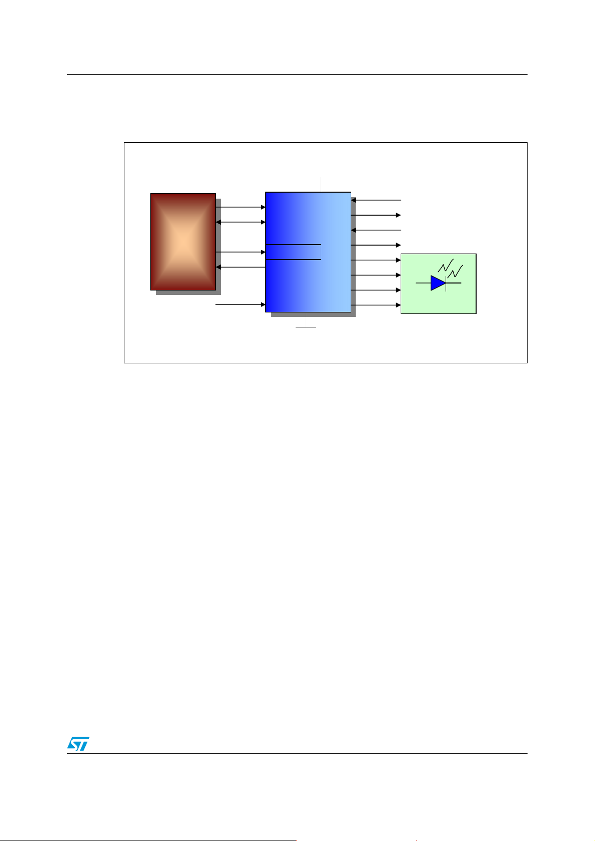
1 STMPE801 Device features
Figure 1. Concept of GPIO Port Expander
VCC VIO
Processor
CLOCK
DATA
ADDRESS
INT
RST_N
STMPE801
GPIO 0
GPIO 1
GPIO 2
GPIO 3
GPIO 4
GPIO 5
GPIO 6
GPIO 7
Hotke
Chi
Enable
erature Sensor
Tem
Control Signal/Ext.Interrupt
LED BANK
GND
– Low CPU utilization (Interrupts available and so no Polling!)
– Configurable Hotkey Detection on each GPIO
– Flexibility in configuration of each of the eight GPIOs
– Simpler communication with CPU (just two I
2
C lines)
– Low power consumption with ultra low standby current (< 1 µA)
– IO and core voltages from 1.65 V up to 3.6 V
– Interrupt output (open drain) pin
– No external clock input required
– Small package QFN16 - 16 pins 1.8 mm x 2.6 mm, making it optimal for use in
portable application like mobile phones with critical space constraints.
The STMPE801 offers great flex ibility as each I/O can be independently configured as input
or output. The eight GPIOs can be connected externally to different modules like LEDs ,
temperature sensors, chip selects for other devices, or as interrupt inputs from other
devices.
This device has been designed with very low quiescent current in standby mode and
includes a Hot Key detection for each I/ O to optimize the power consumption of the IC.
3/13
Page 4
Pin description of STMPE801 AN2466
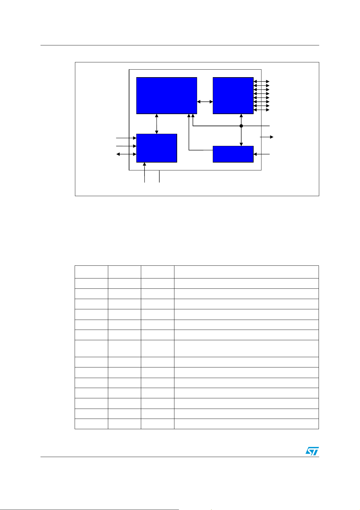
Figure 2. Block diagram of STMPE801
GPIO Controller
ADDRESS
CLOCK
DATA
2
P
I
P
C
Interface
GND
VCC
2 Pin description of STMPE801
The table below gives a list of all the pins on STMPE801.
Table 1. STMPE801 Pin description
GPIO
0-7
POR
GPIO 0-7
VIO
INT
RESET_N
Pin Name Type Description
1 INT O Interrupt output (open drain)
2 Reset_N I External reset input, active LOW
2
3CLOCKAI
4 ADDRESS I Digital Input for I
5DATAAI
6 VCC - Supply voltage for I
7VIO-
C Serial clock line
2
C slave address (either High or Low)
2
C Serial data line
2
C block
Supply voltage for GPIO controller (Note: VIO must alwa ys
be ≥ VCC)
8 GND - GND
9 GPIO_0 IO GPIO
10 GPIO_1 IO GPIO
11 GPIO_2 IO GPIO
12 GPIO_3 IO GPIO
13 GPIO_4 IO GPIO
14 GPIO_5 IO GPIO
4/13
Page 5

AN2466 Pin description of STMPE801
Table 1. STMPE801 Pin description (continued)
Pin Name Type Description
15 GPIO_6 IO GPIO
16 GPIO_7 IO GPIO
2.1 Power Supply - VCC and VIO
The STMPE801 device operates on two different power supplies, VCC and VIO. Both VCC
and VIO can function in the range of 1.65 V to 3.6 V. This enables a variety of device s to
interface directly to the device without a level translator block.
Proper decoupling capacitors should be used to filt er out the Power supply noise. There are
some critical points to be noted to ensure proper functioning of the device as listed below:
– VCC pin supplies the I
– All other pins are connected to the VIO supply.
– At any time, to conserve power, the VCC can be turned off if there is no I
but at no point, should the VIO be turned off while the VCC is ON.
– The VIO should always be ≥VCC
2
C lines and ADDRESS pin.
2
C activity
2.2 I2C Interface
The port expander STMPE801 can be controlled with just the two I2C lines. All internal
registers can be accessed through this I
below:
2
–I
C Slave device
– Operates on the VCC supply (1.65 V to 3.6 V)
– Compliant to Philip I
– Supports standard (up to 100kbps) and fast (up to 400kbps) modes.
– 7-bit addressing mode supported.
– General call
– Up to two STMPE801 devices can be connected on the same I
The slave address is selected by the state of the ADDRESS pin. The address is read every
time the I
changed on the fly without any need for latching the address into the device at reset.
2
C transaction occurs. This implies the slave address of the device can be
2
C interface. The I2C interface f eatur es are as giv en
2
C specification version 2.1
2
C bus
5/13
Page 6

Pin description of STMPE801 AN2466
Figure 3. STMPE801 Slave address selection
STMPE801
2
C Read/ is done byte by byte. The R/ bit is added as the LSB to the 7-bit
The I
slave address to make up one byte to be sent through the I
Table 2. Valid I
Write
2
C Slave address
W
2
C interface from the master.
ADDRESS
Figure 4. I
pin
0 41h (1000001b) 82h
1 44h (1000100b) 88h
2
C Read/write transaction
7-bit Slave Address
8-bit format to be used
(including R/ bit in LSB)
W
Once the slave address is co nfigured and respondin g correctly, the internal registers can be
accessed through I
2
C Interface.
The SCLK and SDATA are open drain pins and should be provided with a pull- up resistor to
VCC. The VCC can be selected ba sed on t he oper a ting voltage of the I
as either 1.8 V or 3.3 V without any need for an intermediate level translator stage.
6/13
2
C host, for e xam ple
Page 7

AN2466 Pin description of STMPE801
Figure 5. I2C pin structure
INPUT BUFFER
INTERNAL
BLOCKS
PAD
Figure 6. I
2
C line with external pull-up resistors
2.2.1 I2C General call
STMPE801 supports I2C general call based on the following table. When a general call
address of 0x00 with R/ = 0 is sent, the device responds with an acknowledgement and
performs the instruction given by the second byte. The device does not give ACK for any
second byte other than the valid second bytes listed in Table 3.
W
Open
Drain
Buffer
ESD DIODE
Table 3. I2C General call
Second byte Definition
0x06 Slave device should reset and latch in the slave address
0x04 Slave device should latch in the slave address but without reset.
0x0 Not allowed as second byte.
2.3 Reset pin (RESET_N)
The Reset pin is an active low input. It should be tied HIGH to VIO supply in order to start
normal operation of the device. Apart from the RESET_N pin, the device can also be reset
through the "Soft_Reset" bit in the SYSCON register. Writing a '1' to Bit 7 resets the device
and after reset, the bit is cleared to '0' by the Hardware.
7/13
Page 8
Pin description of STMPE801 AN2466
PAD
VIO
N-BUFFER
P-BUFFER
INTERNAL
BLOCKS
ESD DIODE
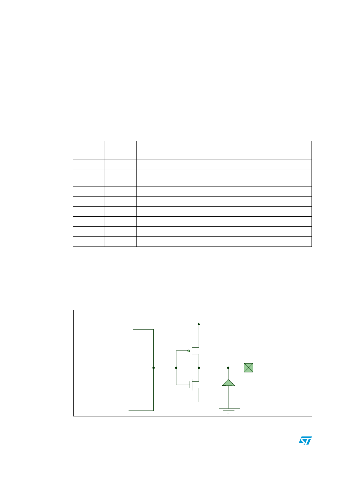
2.4 Interrupt pin (INT)
The interrupt pin is an open drain output pin with a structure similar t o the SCL,SDA pins.
The INT output should be provided with a suitable pull-up resistor to VIO supply. The
interrupt output polarity can be configured as active low or active high by setting Bit 0 of the
SYSCON register. The interrupt output should be enabled by writing a '1' to Bit 2 in the
SYSCON. Even if individual GPIO interrupts are enabled, no interrupt will be generated if
the global INT_Enable bit is not set in the SYSCON. The Interrupt is cleared by reading the
ISGPIOR register (0x09). At reset, the interrupt output is disabled and the polarity is active
LOW.
Table 4. SYSCON register
Bit
7 0 SoftReset Writing ‘1’ to this bit causes a soft reset of the device
60I
50
40
30
2 0 INT_Enable ‘1’ to enable, ‘0’ to disable INT output
10
0 0 INTPolarity ‘1’ for active HI, ‘0’ for active LOW
2.5 GPIO Pins
All 8 GPIO lines are configured as inputs at power-on/reset and are independent of each
other and can be individually programmed as input or output. Unused GPIOs should be
configured as outputs to minimize power consumption.
Figure 7. GPIO pin struct ur e
Reset
value
Name Description
2
C_SHDN
Writing ‘1’ to this bit shuts down the I
valid I2C clock.
2
C block on the next
8/13
Page 9

AN2466 Pin description of STMPE801
2.5.1 Configuring GPIO registers
The GPIO pin direction can be selected as input o r out pu t by writing into the GPDR register
(0x12).
Table 5. GPIO Direction register
GPDR
Bit76543210
IO_7 IO_6 IO_5 IO_4 IO_3 IO_2 IO_1 IO_0
Reset
value
Bits Name Description
7:0 GPIO[x]
00000000
‘0’: The corresponding GPIO pin is set to Input.
‘1’: The corresponding GPIO pin is set to Output.
The GPIO output state can be set high or low by writing into the corresponding bit in the
GPSR register (0x11).
Table 6. GPIO State register
GPSR
Bit76543210
IO_7 IO_6 IO_5 IO_4 IO_3 IO_2 IO_1 IO_0
Reset
value
Bits Name Description
7:0 GPIO[x]
00000000
‘0’: The corresponding GPIO output is set LOW
‘1’: The corresponding GPIO output is set HIGH
If the GPIO is configured as an input, the pin state is monitored by reading the
corresponding bit in the GPMR register (0x 10 ).
Table 7. GPIO Monitor register
GPMR
Bit76543210
IO_7 IO_6 IO_5 IO_4 IO_3 IO_2 IO_1 IO_0
Reset
value
Bits Name Description
7:0 GPIO[x]
00000000
Reading ‘0’: The corresponding GPIO input state is LOW
Reading ‘1’: The corresponding GPIO input state is HIGH
Each GPIO can be individually programmed to generate an interrupt on change of state.
9/13
Page 10
Pin description of STMPE801 AN2466
K
2.5.2 GPIO Level shifting feature
In STMPE801, all GPIO pins are connected to the VIO supply. At reset, all GPIO pins are
LOW and if configured as output, the GPIO pin s reach HIGH state only if a '1' is written to
the corresponding bit in the GPSR register. The HIGH state corresponds to the VIO supply
level. This provides a useful level shifting fe ature without using an explicit level translator
device.
For example, low-voltage processors (Example: 1.8V base-band processors) can directly
control interfacing modules of much higher operating voltages (example 3.6 V drivers)
simply by setting the VIO supply of STMPE801 to the required v oltage and setti ng the GPIO
High/Low by writing into the GPIO registers through the I
Figure 8. GPIO Level shifting feature
2
C interface.
1.8V
Host
2.5.3 GPIO-Hot Key feature
A GPIO is known as 'Hot Key' when it is configured to trigger an interruption to the host
whenever the GPIO input changes state from LOW to HIGH or vice versa. This can also be
used to Wake-up the host processor from Sleep mode.
The GPIO is normally pulled high or pulled low externally with resistors. Any subsequent
change in this logic state triggers an interrupt.
– Programming sequence for Hot Key:
1. The required GPIO pin should be configured as input through the GPDR register.
2. The Global Interrupt (Bit 2) should be enabled by writing '1' and the interrupt polarity
should be set (Bit 0) to active low or active high in the SYSCON register.
3. The ISGPIOR register should be read before enabling the GPIO inter rupts in order to
clear any existing interrupt.
4. The individual GPIO interrupts can be enabled by writing '1' into the corresponding bit
in the IEGPIOR register.
5. Now, t he port expander is read y to detect t he change in logic stat e on an y of the GPIOs
and generate an interrupt to the host processor.
6. Each GPIO state change is reported by the corresponding bit in the ISGPIOR register
and the source of interrupt can be identified by reading the ISGPIOR register. This
permits eight different interrupt sources to be connected to the host through the port
expander . I t should be noted that th e change of GPIO state is recorded in t he ISGPIOR
even if the GPIO interrupt is not enabled in the IEGPIOR.
VCC = 1.8V
SCL
SDATA
STMPE801
VIO = 3.6V
GPIO
3.6V
Driver
10/13
Page 11

AN2466 Pin description of STMPE801
Figure 9. Hotkey detection using external pull-up/pull-down resistors on GPIO
2.6 Minimum pulse width
Typically a minimum pulse width of 2 microseconds is required on the GPIO for Hotkey
detection. Any pulse width less than t he stated v alue may not be registered in the ISGPIOR.
2.7 Power saving mode of operation
STMPE801 operates entirely on the I2C clock. When there is no activity on the I2C bus, the
current consumption of the device is extremely low. However, when there is activity on the
2
I
C bus, current consumption increases, e v en if the I2C traffic is not directed to the assign ed
address.
The host system may choose to shut-down the I
the registers is required. This feature allows the current consumption to drop to the
minimum. The host can turn OFF the I
SYSCON register. The I
2
C block shuts down on the next valid clock edge of the I2C clock
signal. In this state, the device cannot be accessed by I
completely.
Note: The ACK from STMPE801 for a I
the SCL goes high. After this duration the device I
released. The I
To turn ON the I
2
C host should sample the ACK within this interval.
2
C block, the system host must reset the STMPE801. This can be
accomplished by an active low signal on the RESET_N pin.
Table 8. Typical current rating (VCC = VIO = 3 V)
Operating modes Typical VIO current consumption at Ta = 25 °C
Normal operation mode with all outputs switching
and continuous activity on I
2
I
C Shutdown mode <10 nA
2
C block by writing '1' into the I2C_SHDN bit in the
2
C SHDN command is kept low only f or aroun d 250 µs after
2
C bus
2
C block in the STMPE801, if no access to
2
C, as the I2C block has shut down
2
C block shuts down and the SDA line is
~ 10 µA
11/13
Page 12

Conclusion AN2466
2.8 Power-Up sequence
1. The GND pin of the device should be grounded first. First ground the GND pin.
2. The Reset_N pin should be connected to VIO through a w eak pull-up r esistor. Connect
the Reset_N pin to VIO through a weak pull-up resistor.
3. The I2C lines, SCL and SDATA should be connected to the host. Connect the I
SCL and SDATA to the host. Both lines should have pull-up resistors to VCC.
4. The ADDRESS pin should be connected to GND or VCC as per slave address chosen.
Connect the ADRESS pin to GND or VCC according to the slave address chosen. This
can also be accomplished by using external weak pull-up and pull-down resistors on
those two pins or by driving directly from the host.
5. Both VCC and VIO should be supplied through suitable decoupling capacitors.
6. The INT pin should be pulled high to VIO through a weak pull-up resistor. Pull the INT
pin high to VIO through a weak pull-up resistor.
7. With these minimal connections, the device functions in normal mode providing I
access to the internal registers. All GPIOs are in default input mode.
● Tips for hardware trouble shooting:
If the device does not function at the end of the power-up sequence provided above, the
following tips can be used for troubleshooting.
1. All pins are provided with an internal reverse biased ESD protection diode to GND. The
connectivity of the pins vs. GND can be verified.
2
2. I
C clock frequency can be reduced or incr eased to observe the corresponding change
in the current consumption of the device. If there is no change, the device connections
should be verified again.
2
C lines,
2
C
3 Conclusion
The STMPE801 is a very versatile device that can be used to reduce the load on the CPU
and expand the number o f IOs available for the processor. The small size and simple
configuration makes it a very attractive proposition for high-end, portable applications like
smart phones. This application note provided the setup information to interface this device
to a digital engine. The GPIOs in STMPE801 can also be used to perform special functions
like key-pad matrix scanning by using suitable software keypad controller routines on the
host processor. (Refer also application note AN2421: Using the STMPE801 as a keypad
controller)
4 Revision history
Table 9. Revision history
Date Revision Changes
23-Mar-2007 1 Initial release
12/13
Page 13

AN2466
Please Read Carefully:
Information in this document is provided solely in connection with ST products. STMicroelectronics NV and its subsidiaries (“ST”) reserve the
right to make changes, corrections, modifications or improvements, to this document, and the products and services described herein at any
time, without notice.
All ST products are sold pursuant to ST’s terms and conditions of sale.
Purchasers are solely res ponsibl e fo r the c hoic e, se lecti on an d use o f the S T prod ucts and s ervi ces d escr ibed he rein , and ST as sumes no
liability whatsoever relati ng to the choice, selection or use of the ST products and services described herein.
No license, express or implied, by estoppel or otherwise, to any intellectual property rights is granted under this document. If any part of this
document refers to any third pa rty p ro duc ts or se rv ices it sh all n ot be deem ed a lice ns e gr ant by ST fo r t he use of su ch thi r d party products
or services, or any intellectua l property c ontained the rein or consi dered as a warr anty coverin g the use in any manner whats oever of suc h
third party products or servi ces or any intellectual property contai ned therein.
UNLESS OTHERWISE SET FORTH IN ST’S TERMS AND CONDITIONS OF SALE ST DISCLAIMS ANY EXPRESS OR IMPLIED
WARRANTY WITH RESPECT TO THE USE AND/OR SALE OF ST PRODUCTS INCLUDING WITHOUT LIMITATION IMPLIED
WARRANTIES OF MERCHANTABILITY, FITNESS FOR A PARTICUL AR PURPOS E (AND THEIR EQUIVALE NTS UNDER THE LAWS
OF ANY JURISDICTION), OR INFRINGEMENT OF ANY PATENT, COPYRIGHT OR OTHER INTELLECTUAL PROPERTY RIGHT.
UNLESS EXPRESSLY APPROVED IN WRITING BY AN AUTHORIZED ST REPRESENTATIVE, ST PRODUCTS ARE NOT
RECOMMENDED, AUTHORIZED OR WARRANTED FOR USE IN MILITARY, AIR CRAFT, SPACE, LIFE SAVING, OR LIFE SUSTAINING
APPLICATIONS, NOR IN PRODUCTS OR SYSTEMS WHERE FAILURE OR MALFUNCTION MAY RESULT IN PERSONAL INJ URY,
DEATH, OR SEVERE PROPERTY OR ENVIRONMENTAL DAMAGE. ST PRODUCTS WHICH ARE NOT SPECIFIED AS "AUTOMOTIVE
GRADE" MAY ONLY BE USED IN AUTOMOTIVE APPLICATIONS AT USER’S OWN RISK.
Resale of ST products with provisions different from the statements and/or technical features set forth in this document shall immediately void
any warranty granted by ST fo r the ST pro duct or serv ice describe d herein and shall not cr eate or exten d in any manne r whatsoever , any
liability of ST.
ST and the ST logo are trademarks or registered trademarks of ST in various countries.
Information in this document su persedes and replaces all information previously supplied.
The ST logo is a registered trademark of STMicroelectronics. All other names are the property of their respective owners.
© 2007 STMicroelectronics - All rights reserved
STMicroelectronics group of compan ie s
Australia - Belgium - Brazil - Canada - China - Czech Republic - Finland - France - Germany - Hong Kong - India - Israel - Italy - Japan -
Malaysia - Malta - Morocco - Singapore - Spain - Sweden - Switzerland - United Kingdom - United States of America
www.st.com
13/13
 Loading...