

Page 1

AN2455
Application note
STWPLLSim phase noise and settlin g time sim ulator for STW8110x
Application and scope
The STWPLLSim tool helps the end user to design the optimal loop filter for the STW81101x
synthesizers. It provides a very accurate estimation of the overall phase noise and settling
time performances, allowing the user to interactively compare measurements with simulated
performance.
July 2007 Rev 2 1/14
www.st.com
Page 2
Installation AN2455
1 Installation
The STWPLLSim software is written in Java and designed to run on Windows 2000/XP. To
perform time domain simulations, STWPLLSim requires the MATLAB Component Runtime
(MCR) Libraries (Copyright 1984-2005, The MathWorks, Inc. See
http://www.mathworks.com/access/helpdesk/help/toolbox/compiler/index.html?/access/help
desk/help/toolbox/compiler/f12-999353.html
Run
SETUP.bat
to install STWPLLSim.
).
2 Main form
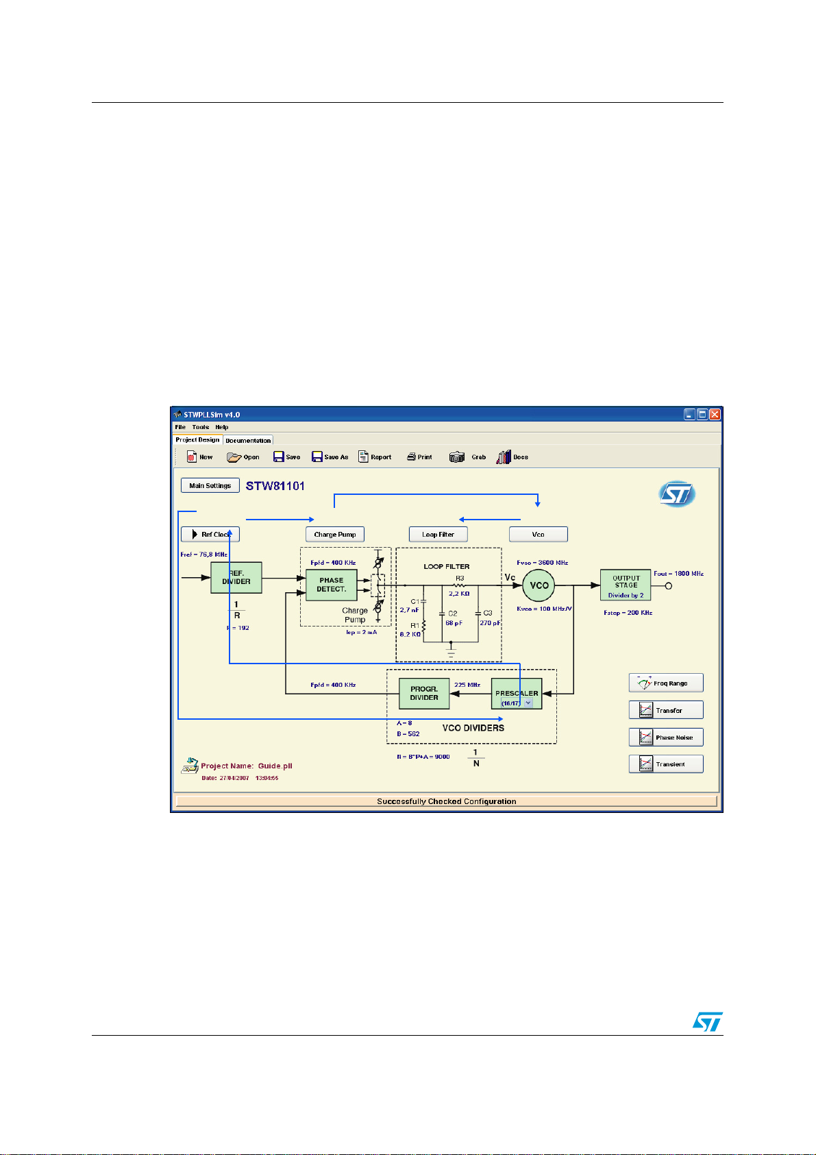
Figure 1. STWPLLSim: main form and project flow
1
3
4
6
2.1 Creating and managing projects
New and Open buttons allow the user to create a new project or to open an existing one.
The project can be save d by pressing the Save / Save As buttons.
5
2
2/14
Page 3

AN2455 Main form
2.2 Project flow
These are the steps to follow in using STWPLLSim, as shown in
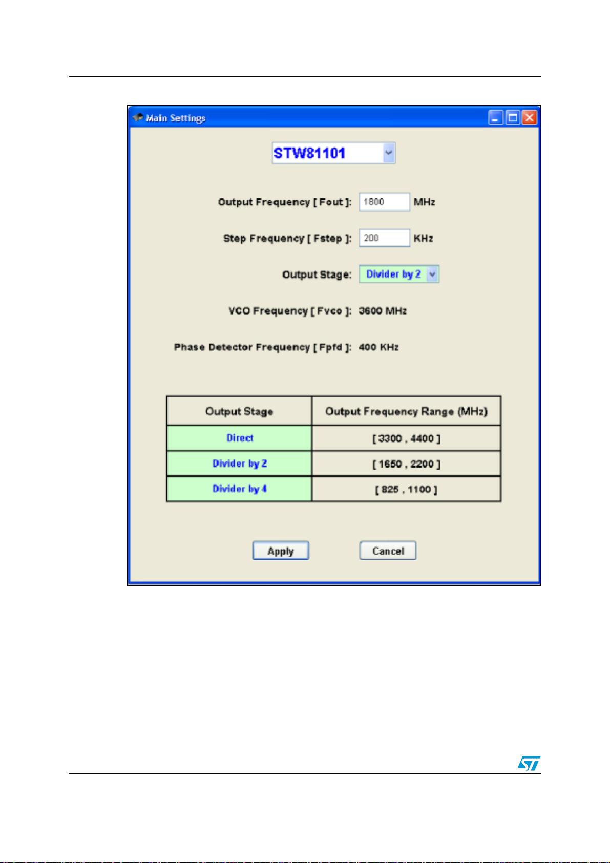
1. Main settings (see the screenshot in
a) Device choice (STW81101, STW81102, STW81103)
b) Output frequency [MHz]
c) Frequency step [kHz]
d) Output stage (direct output, divider by 2, divider by 4)
e) VCO and phase detector frequencies are calculated from the inserted data.
f) A table helps to choose the correct output stage depending on the desired output
frequency and the selected device.
Figure 2
):
Figure 1
:
3/14
Page 4
Main form AN2455
Figure 2. Main settings
1a
1b
1c
1d
1e
1f
4/14
Page 5
AN2455 Main form
2. Prescaler: select the prescaler (either 16/17 or 19/20).
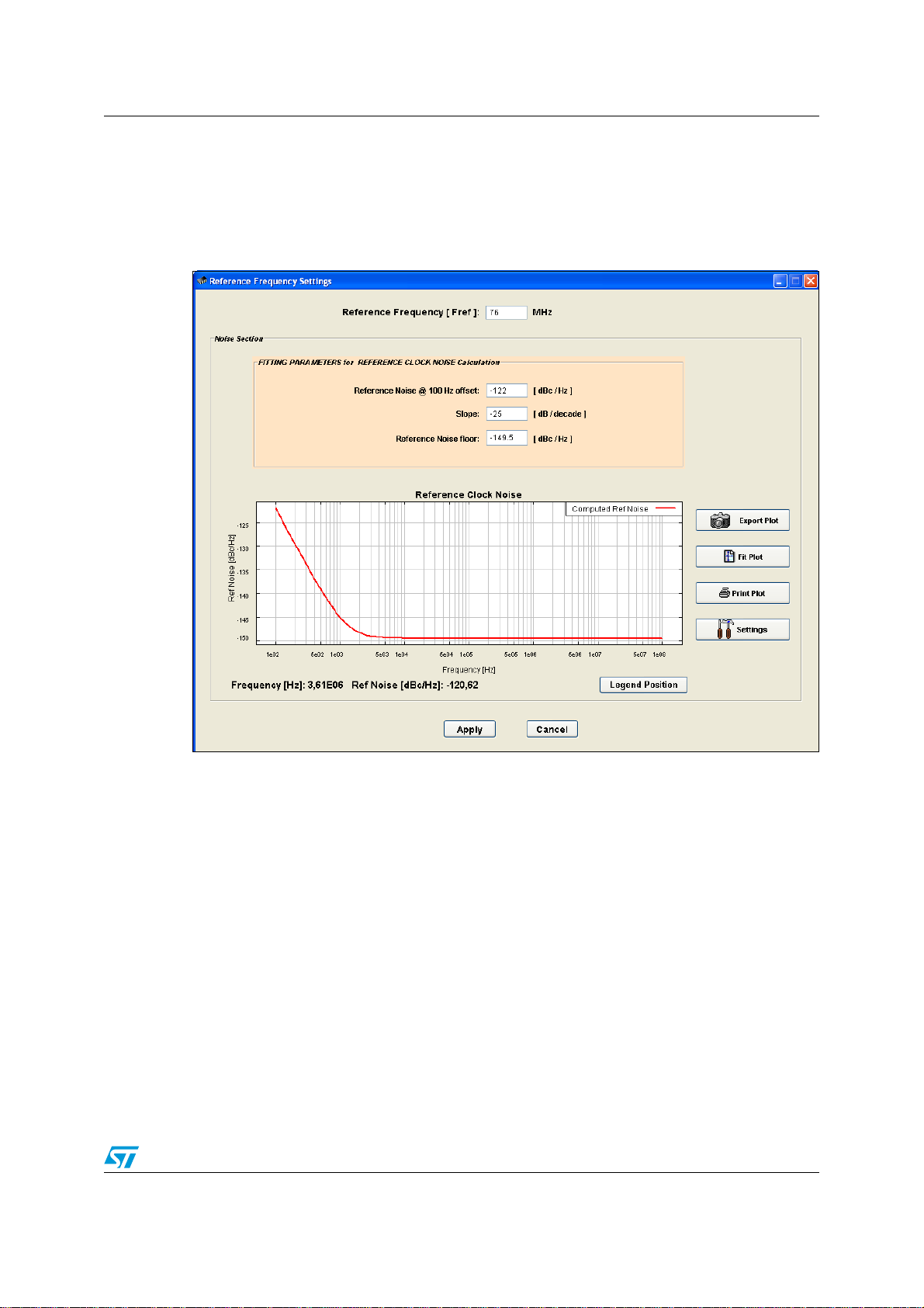
3. Reference clock (see the screenshot in
Figure 3
):
a) Reference frequency
b) Fitting parameters for phase noise performance
Figure 3. Reference clock settings
3a
3b
5/14
Page 6
Main form AN2455
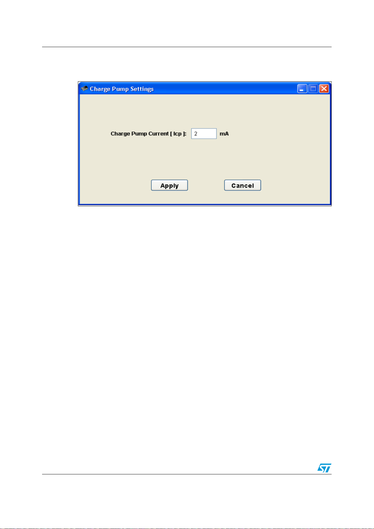
4. Charge pump current [mA] (see the screenshot in
Figure 4
):
Figure 4. Charge pump current settings
4
5. VCO (see the screenshot in
Figure 5
):
a) The VCO frequency set in the main settings form is shown.
b) A typical VCO gain is set depending on the VCO frequency. This value can be
changed by the user.
c) A default or a user measure file can be loaded for the noise calculation.
6/14
Page 7

AN2455 Main form
Figure 5. VCO settings
5a
5b
5c
7/14
Page 8

Main form AN2455
6. Loop filter (see the screenshot in
a) Loop filter network:
- 2nd order
- 3rd order
b) PLL specifications:
- Suggested loop BW
- Suggested (and default) phase margin = 48° (best trade-off between phase noise
and settling time performance)
c) Suggested or user defined values for resistances and capacitances can be used.
Valid unit prefixes are "K" for resistances and "n" and "p" for capacitances.
Figure 6. Loop filter settings forms (2nd and 3rd order)
≤ F
comp
Figure 6
/10
):
6a
6b
6c
8/14
Page 9

AN2455 Waveform viewers
3 Waveform viewers
Waveform viewers are available for transfer functions, phase noise and transient response.
3.1 Transfer functions
The magnitude and phase of the following transfer functions can be plotted:
1. Loop filter
2. PLL open loop
3. PLL closed loop
Figure 7. Transfer function waveform viewer
1
2
3
9/14
Page 10
Waveform viewers AN2455
After selecting the waveforms to plot, press the Plot Selected Curves button. You can
modify the frequency range from the main form by clicking the Freq Range button.
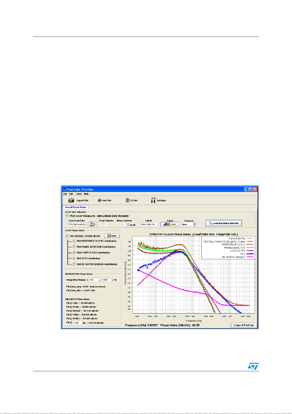
3.2 Phase noise
The following functions are available in the phase noise waveform viewer:
1. Plot the overall phase noise and the following contributions:
– reference clock
– phase detector
– loop filter
–VCO
– RF output divider
2. Save the overall phase noise to a text file.
3. Load user measure/simulated data from a text file.
4. Calculate the integrated phase noise by inserting the integration range limits and
pressing Enter. “K” and “M” are valid unit prefixes for the frequency.
5. Calculate phase noise values for five fixed frequencies and for one user frequency.
You can modify the frequency range from the main form by clicking the Freq Range button.
Figure 8. Phase noise waveform viewer
3
1
2
4
5
10/14
Page 11

AN2455 Waveform viewers
3.3 Transient response
The step time response is plotted and the following parameters can be set:
1. Time unit (μs or ms)
2. Time window: if the specified time window value is lower than the settling time, a
warning message is shown.
3. Points
4. Settling time (frequency error, in ppm, with respect to the F
5. Zoom on settling region (default: on)
final value)
out
The VCO calibration time is calculated according to the F
in the settling time value.
Figure 9. Transient response waveform viewer
1
2
4
3
5
value and taken into account
comp
11/14
Page 12
Report generation and documentation AN2455
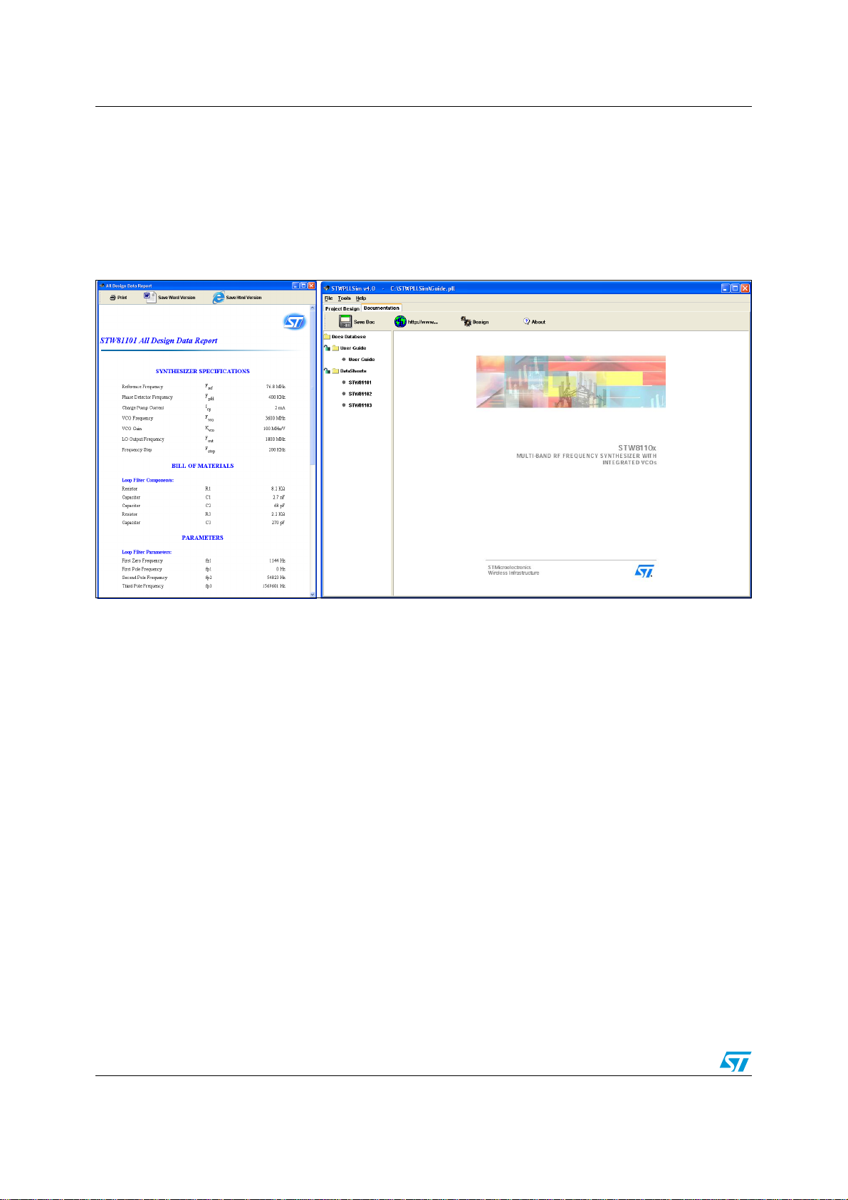
4 Report generation and documentation
A report containing the synthesizer specification, the bill of materials and the design
parameters can be generated by the tool.
The documentation form contains datasheets and application notes.
Figure 10. Design data report and documentation form
12/14
Page 13

AN2455 Revision history
5 Revision history
Table 1. Document revision history
Date Revision Changes
19-Jul-2007 1 Initial release.
20-Jul-2007 2 Corrected the numbering in
Figure 2: Main settings
.
13/14
Page 14

AN2455
Please Read Carefully:
Information in this document is provided sole ly in connecti on with ST produ cts. STMicro electroni cs NV and its subsi diaries (“ST ”) reserve the
right to make changes , cor recti ons , modif ic ations or improv ement s, t o th is documen t, and the prod ucts an d servic es des crib ed he rein a t any
time, without notice.
All ST products are sold pursuant to ST’s terms and conditions of sale.
Purchasers are solely responsible for the choice, selection and use of the ST products and services described herein, and ST assumes no
liability whatsoever rel ating to the choice, selection or use of the ST products and services described herein.
No license, express or implied, by estoppel or otherwise, to any int ellectual property rights is granted under this document. If any part of this
document refers to any third party products or services it shall not be deemed a license grant by ST for the use of such third party products
or services, or any intellectual property contained therein or considered as a warranty covering the use in any manner whatsoever of such
third party products or services or any intellectual property contained therein.
UNLESS OTHERWISE SET FORTH IN ST’S TERMS AND CONDITIONS OF SALE ST DISCLAIMS ANY EXPRESS OR IMPLIED
WARRANTY WITH RESPECT TO THE USE AND/OR SALE OF ST PRODUCTS INCLUDING WITHOUT LIMITATION IMPLIED
WARRANTIES OF MERCHANTABILITY, FITNESS FOR A PARTICULAR PURPOSE (AND THEIR EQUIVALENTS UNDER THE LAWS
OF ANY JURISDICTION), OR INFRINGEMENT OF ANY PATENT, COPYRIGHT OR OTHER INTELLECTUAL PROPERTY RIGHT.
UNLESS EXPRESSLY APPROVED IN WRITING BY AN AUTHORIZED ST REPRESENTATIVE, ST PRODUCTS ARE NOT
RECOMMENDED, AUTHORIZED OR WARRANTED FOR USE IN MILITARY, AIR CRAFT, SPACE, LIFE SAVING, OR LIFE SUSTAINING
APPLICATIONS, NOR IN PRODUCTS OR SYSTEMS WHERE FAILURE OR MALFUNCTION MAY RESULT IN PERSONAL INJURY,
DEATH, OR SEVERE PROPERTY OR ENVIRONMENTAL DAMAGE. ST PRODUCTS WHICH ARE NOT SPECIFIED AS "AUTOMOTIVE
GRADE" MAY ONLY BE USED IN AUTOMOTIVE APPLICATIONS AT USER’S OWN RISK.
Resale of ST products with prov isions differen t from the state ments and/or tec hnical featur es set forth in th is document shall immediatel y void
any warranty granted by ST for the ST product or service described herein and shall not create or extend in any manner whatsoever, any
liability of ST.
ST and the ST logo are trademark s or registered trademarks of ST in various countries.
Information in this document su persedes and replaces all information previously supplied.
The ST logo is a registered trade mark of STMicroelectronics. All other names are the property of their respective owners.
© 2007 STMicroelectronics - All rights reserv ed
STMicroelectronics group of companies
Australia - Belgium - Brazil - Canada - China - Czech Republic - Finland - France - Germany - Hong Kong - India - Israel - Italy - Japan -
Malaysia - Malta - Morocco - Singapore - Spain - Sweden - Switzerland - United Kingdom - United States of America
www.st.com
14/14
 Loading...