

Page 1
AN2454
Application note
Universal input voltage power supply for ESBT based
breaker and metering applications
Introduction
This document describes how to design a 3-phase power supply with the UC3845B PWM
driver and the new STC04IE170 ESBT as main switch. It is associated with the release of
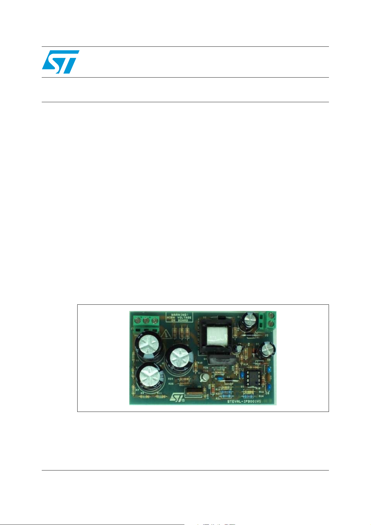
the STEVAL-IPB001V1 demo board (see figure below). The design is a complete solution
for the 2 W single output SMPS, which is widely used as a power supply in breaker
applications. However, the design method can also be applied to an SMPS suitable for 3phase power metering applications, as it can easily be upgraded for higher output power.
In this report particular attention has been paid to the ESBT base driving circuit, where
some useful methods have been investigated to better optimize power dissipation (see
Section 6: Base driving circuit design).
The influence of the parasitic capacitances of the transformer on the ESBT is also explained
in detail (see Section 3: Parasitic capacitances and related issues). In addition, an active
start-up circuit has been implemented on the demo board to optimize the converter
efficiency, is also described (see Section 7: Active start-up circuit). A dedicated active
component (the Darlington Q3) has been developed to support the very high voltage
required (see Figure 1).
Finally, the most important waveforms and thermal results are given in Section 8:
Experimental results: waveforms and Section 9: Experimental results: efficiency and special
considerations. They demonstrate the benefits of using this solution with the start-up circuit.
Refer to AN1889 for the overall design of an auxiliary power supply using an ESBT.
STEVAL-IPB001V1 demo board
December 2006 Rev 1 1/24
www.st.com
Page 2

Contents AN2454
Contents
1 Design specifications and schematic diagram . . . . . . . . . . . . . . . . . . . 4
2 Flyback stage . . . . . . . . . . . . . . . . . . . . . . . . . . . . . . . . . . . . . . . . . . . . . . . 6
3 Parasitic capacitances and related issues . . . . . . . . . . . . . . . . . . . . . . . 8
4 Fine tuning of the application . . . . . . . . . . . . . . . . . . . . . . . . . . . . . . . . . 9
5 Transformer design characteristics . . . . . . . . . . . . . . . . . . . . . . . . . . . . 11
6 Base driving circuit design . . . . . . . . . . . . . . . . . . . . . . . . . . . . . . . . . . 11
7 Active start-up circuit . . . . . . . . . . . . . . . . . . . . . . . . . . . . . . . . . . . . . . . 13
8 Experimental results: waveforms . . . . . . . . . . . . . . . . . . . . . . . . . . . . . 16
9 Experimental results: efficiency and special considerations . . . . . . 19
10 Revision history . . . . . . . . . . . . . . . . . . . . . . . . . . . . . . . . . . . . . . . . . . . 23
2/24
Page 3

AN2454 List of figures
List of figures
Figure 1. Schematic diagram of the SMPS . . . . . . . . . . . . . . . . . . . . . . . . . . . . . . . . . . . . . . . . . . . . . 5
Figure 2. Small signal equivalent circuit. . . . . . . . . . . . . . . . . . . . . . . . . . . . . . . . . . . . . . . . . . . . . . . . 8
Figure 3. Current sense circuit (a) and waveform of sense resistor ( b) . . . . . . . . . . . . . . . . . . . . . . . 9
Figure 4. The normal operation waveforms of output pulse and current spike . . . . . . . . . . . . . . . . . 10
Figure 5. ESBT driving circuit . . . . . . . . . . . . . . . . . . . . . . . . . . . . . . . . . . . . . . . . . . . . . . . . . . . . . . 11
Figure 6. h
Figure 7. Start-up circuit. . . . . . . . . . . . . . . . . . . . . . . . . . . . . . . . . . . . . . . . . . . . . . . . . . . . . . . . . . . 14
Figure 8. Minimum input voltage: storage highlighted . . . . . . . . . . . . . . . . . . . . . . . . . . . . . . . . . . . . 16
Figure 9. Minimum input voltage: switch-on highlighted . . . . . . . . . . . . . . . . . . . . . . . . . . . . . . . . . . 16
Figure 10. Minimum input voltage 1 . . . . . . . . . . . . . . . . . . . . . . . . . . . . . . . . . . . . . . . . . . . . . . . . . . . 16
Figure 11. Minimum input voltage 2 . . . . . . . . . . . . . . . . . . . . . . . . . . . . . . . . . . . . . . . . . . . . . . . . . . . 16
Figure 12. Minimum input voltage: switch-off highlighted . . . . . . . . . . . . . . . . . . . . . . . . . . . . . . . . . . 17
Figure 13. 560V input voltage 1 . . . . . . . . . . . . . . . . . . . . . . . . . . . . . . . . . . . . . . . . . . . . . . . . . . . . . . 17
Figure 14. 560V input voltage 2 . . . . . . . . . . . . . . . . . . . . . . . . . . . . . . . . . . . . . . . . . . . . . . . . . . . . . . 17
Figure 15. 560V input voltage: switch-on highlighted . . . . . . . . . . . . . . . . . . . . . . . . . . . . . . . . . . . . . 18
Figure 16. 560V input voltage: switch-off highlighted . . . . . . . . . . . . . . . . . . . . . . . . . . . . . . . . . . . . . 18
Figure 17. 1050V input voltage 1 . . . . . . . . . . . . . . . . . . . . . . . . . . . . . . . . . . . . . . . . . . . . . . . . . . . . . 18
Figure 18. 1050V input voltage 2 . . . . . . . . . . . . . . . . . . . . . . . . . . . . . . . . . . . . . . . . . . . . . . . . . . . . . 18
Figure 19. 1050V input voltage: switch-off highlighted . . . . . . . . . . . . . . . . . . . . . . . . . . . . . . . . . . . . 18
Figure 20. 1050V input voltage: switch-on highlighted . . . . . . . . . . . . . . . . . . . . . . . . . . . . . . . . . . . . 18
Figure 21. 110 Vac envelope . . . . . . . . . . . . . . . . . . . . . . . . . . . . . . . . . . . . . . . . . . . . . . . . . . . . . . . . 19
Figure 22. 220 Vac envelope . . . . . . . . . . . . . . . . . . . . . . . . . . . . . . . . . . . . . . . . . . . . . . . . . . . . . . . . 19
Figure 23. 420 Vac envelope . . . . . . . . . . . . . . . . . . . . . . . . . . . . . . . . . . . . . . . . . . . . . . . . . . . . . . . . 20
Figure 24. 480 Vac envelope . . . . . . . . . . . . . . . . . . . . . . . . . . . . . . . . . . . . . . . . . . . . . . . . . . . . . . . . 20
Figure 25. 600 Vac envelope . . . . . . . . . . . . . . . . . . . . . . . . . . . . . . . . . . . . . . . . . . . . . . . . . . . . . . . . 20
Figure 26. 760 Vac envelope . . . . . . . . . . . . . . . . . . . . . . . . . . . . . . . . . . . . . . . . . . . . . . . . . . . . . . . . 20
Figure 27. Top view of the STEVAL-IPB001V1 demo board . . . . . . . . . . . . . . . . . . . . . . . . . . . . . . . 22
Figure 28. Bottom view of the STEVAL-IPB001V1 demo board . . . . . . . . . . . . . . . . . . . . . . . . . . . . . 23
curve from datasheet STC04IE170HP, section 2.1, figure 3 . . . . . . . . . . . . . . . . . . . . 12
FE
3/24
Page 4

Design specifications and schematic diagram AN2454
1 Design specifications and schematic diagram
Ta bl e 1 lists the converter specifications and main parameters of the STEVAL-IPB001V1
demo board.
Table 1. Converter specifications and main parameters of the STEVAL-IPB001V1
demo board
Symbol Description Values
V
inmin
V
inmax
V
P
out max
P
out min
out
Rectified minimum input voltage 150
Rectified maximum input voltage 1200
Output voltage 24V/83mA
Maximum output power 2W
Minimum output power 0.2W
η Converter efficiency 60%
F Switching frequency ≅ 50kHz
V
V
fl
spike
Max over voltage limited by clamping circuit 150V
Reflected flyback voltage 150V
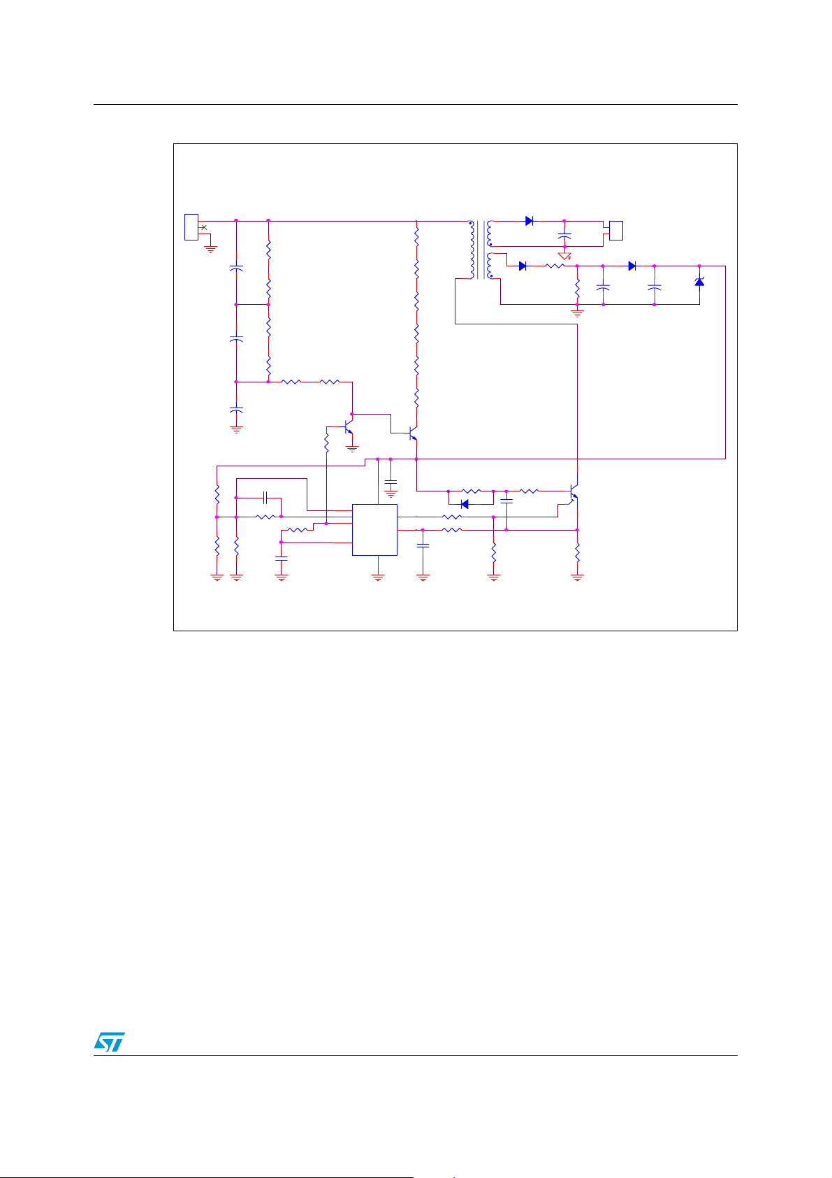
A schematic diagram of the SMPS is given in Figure 1 The most relevant components are:
● HV ESBT main switch and simple driving circuit (see Section 6: Base driving circuit
design).
● Active start-up circuit with HV bipolar Darlington (see Section 7: Active start-up circuit) .
● A specially constructed transformer, with very low parasitic capacitance.
4/24
Page 5
AN2454 Design specifications and schematic diagram
Figure 1. Schematic diagram of the SMPS
J1
CON3
7
8
2
1
R22
10k
D1
STTH110
D2
STTH110
R26 10
C7
10nF
+
R3 1
4
2
4
R17 22
R19 1k
C9
820pF
T1
5
R15 3.3k
D4
STTH110
1
2
3
R14
18k
R20
100k
C2
+
33uF450V
C5
+
33uF 450V
C6
+
33uF 450V
C8 100p
R16 150k
R21
3.9K
R1
1M 1/8W
R4
1M 1/8W
R7
1M 1/8W
R9
1M 1/8W
R18 2.2k
R11
1M 1/8W
C10
12nF
R12
1M 1/8W
2
R13
680k
31
Q2
PN2222A
U1
2
VFB
1
COMP
8
VREF
4
RT/CT
UC3845B
7
VCC
SENSE
GND
5
OUT
1
100nF
C11
6
3
R2
10k 1/4W
R5
10k 1/4W
R8
10k 1/4W
R10
10k 1/4W
R24
10k 1/4W
R25
10k 1/4W
23
Q3
STP03D200
C1
220uF 35V
R6
10k
13
Q4
STC04IE170HP
R23
6.8
CON2
2
1
J2
C4
+
47uF 25V
D3
1N4148
+
C3
330uF 25V
D5
20V
5/24
Page 6

Flyback stage AN2454
2 Flyback stage
In this section, only the main steps of the flyback stage are given. For more detailed
guidelines on Discontinuous Conduction Mode (DCM) flyback converter design, refer to
AN1889.
First, the transformer turn ratio, N
, must be calculated. NP and NS are the respective
P/NS
number of primary and secondary windings. Calculation of the turn ratio is correlated to the
maximum voltage rating of the transistor which is used as the primary switch. The voltage of
the power switch collector, V
, for flyback operation is given by:
T
Equation 1
N
P
-------
N
+()• Vfl==
V
oVFdiode,
+()V
V
oVF diode,
S
where
minarg+++=
spike
the flyback voltage
where V
VTV
is the over voltage limited by the clamp network. It must be chosen so that the
spike
N
-------
N
dcmax
P
S
total voltage across the power switch does not exceed the maximum breakdown voltage of
the power switch device (see Equation 1).
Once the V
voltage is fixed, the designer must choose the flyback voltage taking
spike
account of various voltage capabilities available from standard transistors. The higher the
flyback voltage the higher the exploitable maximum duty cycle i.e. a higher duty cycle at
fixed output power leads to a lower I
current. This improves overall efficiency of the
RMS
primary side, leading to easier design of wide input range voltage converters.
ESBTs, which have breakdown voltage capabilities as high as 2200V, offer designers a
valuable tool to simplify projects from an early stage.
For the STEVAL-IPB001V1 demo board using the STC04IE170HP switch, the following
parameters must be set:
● Margin = 200V.
● V
From Equation 1, the flyback vlotage (V
spike
= 150V.
) gives a result of 150 V. The transformer turn ratio
fl
may then be calculated using Equation 2.
Equation 2
– V
BV V
N
P
--------------------------------------------------------------------------------- -
-------
N
S
6/24
dcmax
V
oVFdiode,
– minarg–
spike
+
1700 1200– 150– 200–
---------------------------------------------------------------- 6===
24 1+
Page 7

AN2454 Flyback stage
Once the turn ratio is calculated, the system must be stabilized to ensure that the converter
operates in discontinuous mode. Equation 3 guarantees that the energy on the primary coil
will be completely transferred to the secondary coil before the next cycle occurs.
Equation 3
N
P
V
dcminTonmax
-------
N
V
S
+()T
oVF diode,
==
resetVflTreset
A safety margin of 20% is recommended to guarantee the complete demagnetization of the
primary side (see Equation 4).
Equation 4
T
– 0.8T
onmaxTreset
=
S
where T
transformer inductance, and T
Combining Equation 3 and Equation 4 , T
is the maximum power-on time, T
onmax
the switching time.
S
the time needed to demagnetize the
reset
, may be calculated using Equation 5:
onmax
Equation 5
Vfl0.8T
T
onmax
------------------------------ -=
V
S
+
dcminVfl
Once output power has been set to 2 W and the desired efficiency to 60%, the operating
switching frequency must be chosen. To do this, a value of 50 kHz should be selected. It is
then necessary to calculate the primary inductance (L
6, input power (P
) may be calculated to give an approximate value which does not account
IN
) of the transformer. Using Equation
P
for losses due to the power switch, the input bridge and the rectified network.
Equation 6
Using Equation 7, L
1
-- -
2
P
1.66P
IN
may be calculated as follows:
P
OUT
------------------------
2
LPI
•
T
1
-- -
V
P
2
------------------------- -===
S
onmax
LPT
2
S
Equation 7
V
dcmin
------------------------------------------ -
L
P
3.33TSP
2
T
onmax
2
11m H≈=
OUT
Peak current, (I
) on the primary side may be calculated using Equation 8.
P
Equation 8
V
dcminTonmax
-------------------------------------
I
P
L
P
110mA≈=
It is also important to determine the maximum primary current, I
and maximum secondary current, I
rms(secondary)
, (see Equation 10) to obtain correct
dimensions for the wire size of the primary windings.
rms(primary)
, (see Equation 9)
7/24
Page 8
Parasitic capacitances and related issues AN2454
)
)
Equation 9
I
T
P
onmax
I
rms primary()
-------
------------------ - 40m A≈=
T
3
S
Equation 10
I
T
S
reset
I
rms ondarysec()
-------
--------------- 240mA≈=
T
3
S
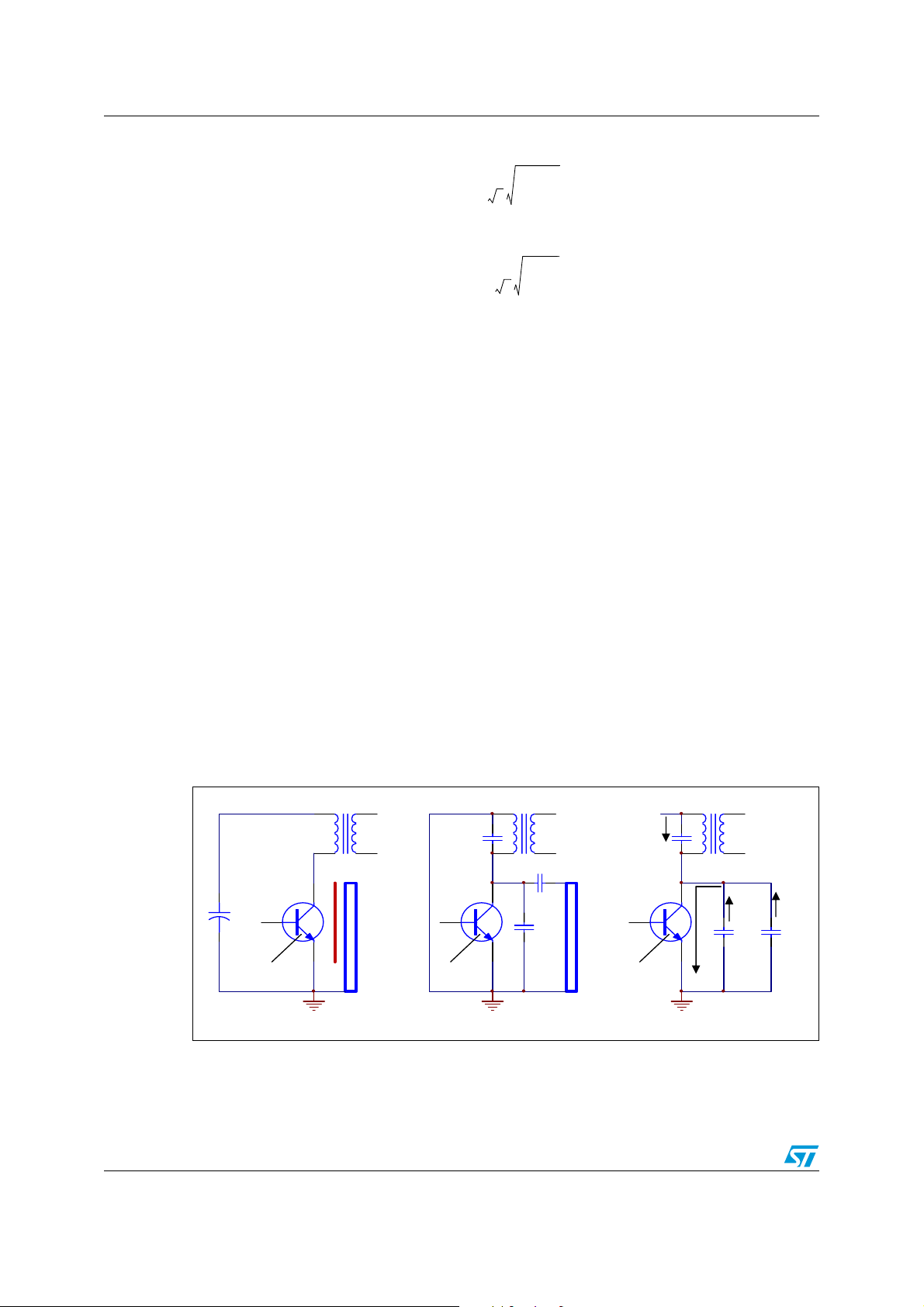
3 Parasitic capacitances and related issues
In a flyback converter stage it is important to take into account the parasitic capacitances
since their influence may affect the correct operation of the converter itself. Figure 1 shows
the main schematic diagram of a flyback converter and Figure 2 shows the small signal
equivalent model.
The parasitic capacitances between the ESBT collector and ground are mainly due to three
components (see Figure 2):
● C
● C
● C
Usually transistors are mounted on a heat-sink by interposing an insulation layer. The heatsink has to be grounded either for safety reasons, or to minimize the RFI so that C
are in the same range as C
C
power dissipation. Large parasitic capacitances may produce noise problems (origin
ringing). Parasitic capacitance are worse at higher input voltages, like those observed in 3phase power supply.
, the primary inter-winding capacitance;
1
, the intrinsic capacitance of the ESBT between its collector and source;
2
, the parasitic capacitance between the collector of the ESBT and the heat-sink.
3
results
and C2. The resulting total parasitic capacitance (C) is equal to
+ C2 + C3. C may be large enough to produce additional and non-negligible switch-on
1
1
3
Figure 2. Small signal equivalent circuit
T
I nsula ion Pad
Heatsink
ESBT
+
Cbus
ESBT
a
The flyback converter of the demo is operated in DCM, thus, before the end of the off-time
the secondary of the transformer has discharged all energy stored in the primary inductance
during the previous cycle.
8/24
C1
C3
C2
T
Ic1
T
C1
Heatsink
ESBT
Ic
b
Ic2 Ic3
C2
C3
Page 9

AN2454 Fine tuning of the application
Considering that the power supply is low, the transistor works without a heat sink, and
consequently C
during switch-on and does not affect system stability. C
effects can be ignored. C2 is related only to additional power dissipation
3
has the most important affect on
1
flyback converter design. It in turn affects:
● Parasitic transformer inter-winding capacitance.
● Layout parasitic capacitance.
Care is needed when designing the layout parastic capacitance and building the
transformer.
4 Fine tuning of the application
Once the design is completed, application parameters and performance are fine tuned by
bench verification.
Bench verification of the current demo board has highlighted that the chosen frequency and
the high input voltage correspond with a very short conductance time. This may cause some
instability or malfunctioning, even with optimized transformer parasitic elements. According
to Equation 11, the maximum conductance time (T
1200 V is:
onmax\@Vdcmax
) at an input voltage of
Equation 11
LPI
P
T
@@
onmaxvbVdcmax
The flyback power supply tends to oscillate at maximum input voltage. The R
------------------ -
V
dcmax
1µs≈=
resistor is in
s
series with the ESBT as shown in Figure 3 and has a current sensing function. The current
waveform often has a large spike at its leading edge (see Figure 4). This is caused by the
charge of the parasitic capacitance C
. Usually, a simple RC filter is used to suppress this
1
transient spike. The RC time constant should approximately equal the current spike
duration, which is usually a few hundred nanoseconds. Values used in the demo board are:
● R
● C
Figure 3. Current sense circuit (a) and waveform of sense resistor ( b)
= 1 kΩ.
cs
= 820 pF.
s
UC384 5
VC C
FB
COMP
VR EF
RT/CT
ESBT
6
OUT
Vcs Vrs
3
ISENSE
Cs
(a) (b )
Rcs
Rs
Spike
Vrs
9/24
Page 10

Fine tuning of the application AN2454
Output Puls e
Ve
Vcs Vcs
S
p
ike
(a ) (b )
Figure 4. The normal operation waveforms of output pulse and current spike
Before RC filter After RC filter
Note that if the filter capacitance is too high, the minimum duty cycle may not be attainable
and consequently there may be oscillations and instabilities. However, there may also be
some instability if the filter capacitance is too small. The reason for this is as follows: energy
transferred from the primary to the secondary side is small if the output pulse is prematurely
terminated during the switching cycle. If this happens for several pulses, the feedback loop
increases the error signal and produces a higher energy that is transferred to the secondary
side. As a result, a higher output pulse is generated and again prematurely ended. Another
disadvantage of a filter capacitance which is too small, is that the power supply may fail at
full load and minimum input voltage. Both problems may be reduced by decreasing the
parasitic capacitance between the collector and ground. This has the effect of smoothing the
current spike during switch-on. In applications where switch-on occurs at very high voltages,
such as single switch power supplies operating at very high input voltage, the high amount
of energy stored in the parasitic capacitances leads to high peak currents and oscillations.
In the 2W SMPS, the current on the switch is very low, and even a very small peak on the
leading edge during switch-on may cause the problems described above. To eliminate this
problem, the parasitic capacitance must be reduced as much as possible by optimizing the
layout and the transformer. When this is accomplished, the above effects can be minimized
futher by additional fine tuning of the switching frequency.
Frequency reduction leads to a higher conduction time since the peak current has to be
higher to develop the same output power. Of course, if frequency reduction is not followed
by an increase in primary inductance, the system goes into deep discontinuous operating
mode.
To stabilize the process following an increase of the primary inductance, there must be a
trade off between the positive effect of a longer conduction time and the negative effect of a
new reduction in the peak current.
In this demo board a switching frequency of 25-30 kHz and an inductance of 13 mH has
been set.
10/24
Page 11

AN2454 Transformer design characteristics
R15 3.3k
R23
6.8
R17 22
C7
10nF
U1
UC3845B
VFB
2
COMP
1
VREF
8
RT/CT
4
SENSE
3
OUT
6
VCC
7
GND
5
C11
100nF
Q4
STC04IE170HP
4
13
2
D4
STTH110
R26 10
5 Transformer design characteristics
The transformer used in this demo board has the part number SRW20EF-E13H003. Its
design is not described in this application note . It is supplied by TDK and shows very low
parasitic capacitance and leakage inductance.
6 Base driving circuit design
In applications such as the SMPS, where the load varies, the current of the ESBT's collector
also fluctuates. To minimize losses on the power switch, a current should be provided on the
base which is proportional to the collector current. It is important to avoid oversaturation of
the device at low load and aim to optimize performance at full load. To achieve this a driving
circuit may be used, with a current transformer, to supply the base with a current
proportional to that of the collector. For additional information about ESBT base driving
methods, refer to AN2131.
Figure 5 shows a simple driving circuit used for the current application. As well as being
simple, it is cost effective and it minimizes power losses.
The first step in designing the base driving circuit is to set the base resistance (R
Bearing in mind that the primary peak current (I
) of the present application is 110 mA (see
P
15
Equation 8 in Section 2), it is possible to calculate the base current required for the
application using the dc current gain (h
) curve in Figure 6. For further information on hFE
FE
curves, refer to datasheet STC04IE170.
Figure 5. ESBT driving circuit
).
11/24
Page 12

Base driving circuit design AN2454
Figure 6. hFE curve from datasheet STC04IE170HP, section 2.1, figure 3
At this current value (110 mA) the gain of the ESBT is about 25 (see Figure 6), so
theoretically the current needed to drive the base should be 4.4 mA (110/25). This is true for
very long conduction times. However, for the present application, a dynamic saturation
phenomenon may occur due to a combination of relatively high switching frequencies (about
30 kHz) and small conduction times (1 µs at full load and maximum input voltage).
The dynamic saturation effect, which is observable in all "bipolar devices" during switch-on
operations, is related to the delay of the voltage drop between collector and emitter in
reaching the static value (V
). In general, the higher the working frequency, the worse
CESAT
the dynamic saturation effect is. A method which is commonly used to moderate this effect,
is to inject the base quickly and heavily with minority carriers, thereby providing a very high
current peak at switch-on. The resulting high base current conflicts with the need not to
oversaturate the device because it impacts badly on switch-off losses. In fact, benefits
obtained at switch-on may actually be a weakness at switch-off.
To summarize, a base current higher than the theoretical value of 4.4 mA has to be provided
to enhance conduction performances by reducing the voltage drop just after switch-on.
However, if the base current is increased arbitrarily, switch-off may be too slow and overly
dissipative. A good trade off may be achieved if the dimensions of the base capacitor are
small enough to provide a very high but short current peak to the base.
Note that during storage time the collector current flows through the base and gets stored in
the base capacitor so that a quasi total recovery of energy is achieved.
Using Equation 12, the time duration of the base current spike ( t
) may be calculated to
PEAK
give an approximate value:
Equation 12
To achieve a T
t
peak
of 300 ns, and since the value of R26 is set to 10 Ω, then capacitor 7 (C7)
peak
=
3R26C
7
may be calculated using Equation 13 to give a value of 10 nF:
Equation 13
C
Knowing that V
12/24
is approximately 15V, R15 may be calculated to give a value of 3.4 kΩ:
CC
t
peak
------------ -
7
3R
10nF==
26
Page 13

AN2454 Active start-up circuit
Equation 14
15V
----------------- -
R
15
4.4mA
3.4kΩ==
The closest commercial value available for R
7 Active start-up circuit
A non-dissipative, active start-up circuit has been implemented to optimize converter
efficiency. The alternative option to use a pure resistive start-up circuit was rejected
because total converter efficiency would have been extremely low due to the low output
power (2 W).
To select the components of the start-up circuit, the following steps should be followed:
1. Find the minimum start-up current (I
to datasheet UC3845B, I
2. Set the maximum start-up resistance (R
driver consumption (see above) and using Equation 15 below.
3. Set the start-up capacitor according to the start-up and UVLO threshold of the
UC3845B and total consumption during start-up time (i.e. the time between the points
when start-up threshold and output and auxiliary steady state voltage are reached).
4. Verify the relevant start-up time and test the wake-up time.
5. Fine tune the necessary components. For example, if wake-up time is too long the
start-up resistors need to be reduced. If start-up time is too long C
Figure 1 may need to be increased.
UC3845B-start-up
is 3.3 kΩ.
15
UC3845B-start-up
) required by the IC driver. Referring
has a value of 0.5 mA.
start-upmax
), paying particular attention to the
(capacitor 3) in
3
Using Equation 15 the maximum start-up resistance (R
start - upmax
) may be calculated:
Equation 15
V
dcmin
R
start upmax–
The additional power dissipation (P
-------------------------------------------- -
I
UC 3845 st a rt– up–
) due to the start-up circuit at maximum input
Rstart
300k Ω==
voltage may then be calculated using Equation 16.
Equation 16
2
1200
However, when V
dc
= V
P
Rstart
= 1200 V, a value of 4.8 W is unacceptable since the maximum
dcmax
-------------------------
300 103•
4.8W==
output power is 2 W.
This problem cannot be solved even if the I
much lower start-up current. Referring to datasheet L
driver is replaced by the L
C
6565
, I
L6565-start-up
which uses a
6565
has a value of 70
µA. Substituting into Equation 17, Equation 18, a value of 0.66 W for the additional power
dissipation is still too high since it represents about 33% of total output power.
13/24
Page 14

Active start-up circuit AN2454
Equation 17
V
dcmin
R
start upmax–
----------------------------------------
I
L6565 st a r t– up–
2.15M Ω==
Equation 18
2
1200
P
Rstart
-------------------------- -
2.15 106•
0.66W==
Clearly, an active start-up circuit is essential to increase converter efficiency. Moreover, it
allows the use of the simplist, low cost PWH driver.
Figure 7 shows the start up circuit used in the present demo board. The start-up resistance
comprises a series of 6 resistors, while C
is in parallel with C3 and C11 (see Figure 1).
start-up
The balance resistances shown in Figure 7, are used to ensure the same voltage drop
across each input capacitor and to supply the current to the base of the Q3 Darlington
before V
reaches the device threshold. During this time V
CC
input of UC3845B is low
REF
and Q2 is off.
When V
reaches the start-up threshold (typically 8.4 V), V
CC
is high (5 V) and Q2 is
REF
turned on. Q3 is turned off which disconnects the start-up current path. The additional
power dissipation under such normal working conditions is due to the balance resistances.
They may be set at very high values.
Figure 7. Start-up circuit
J1
1
2
3
CON3
C2
+
33uF450V
C5
+
33uF 450V
C6
+
33uF 450V
R1
1M 1/8W
R4
1M 1/8W
R7
1M 1/8W
R9
1M 1/8W
1M 1/8W
Balance
Resistance
R11
R12
1M 1/8W
2
31
Q2
PN2222A
R25
R
start-up
10k 1/4W
23
Q3
1
STP03D200
As an active start-up circuit is being used, the start-up current may be over set by fixing the
start-up resistance correctly. However, first the start-up capacitor must be calculated.
14/24
R13
680k
U1
2
VFB
1
COMP
8
VREF
4
RT/CT
UC3845B
7
OUT
VCC
SENSE
GND
5
C11
C
start-up
100nF
6
3
Page 15

AN2454 Active start-up circuit
The start-up capacitor feeds the PWM driver of the UC3845B device until the auxiliary
supply voltage rises. Using the UC3845B datasheet and assuming a start-up time of 10 ms
(which should be validated on the bench), the minimum start-up time (C
start-upmin
) may be
calculated as follows:
Equation 19
C
start upmin–
I
∆Q
UC3845quiescent
--------
------------------------------------------------------------------------ -
∆V
V
start up–
Tstart up–
V
–
UVLO
17m A 10ms•
------------------------------------- -
8.4 7.6–
212.5µF====
If a wake-up time (T
wake-up
) of 1 s is set, as a worst case scenario, T
wake-up
may be
calcluated using Equation 20:
Equation 20
The total start-up current
Equation 21:
T
(I
totstart-up
C
start upmin–
wake up–
---------------------------------------------------------- -=
) needed before start-up may then be calculated using
I
totstart up–
V
start up–
Equation 21
I
totstart up–
Hence, start-up resistance (R
C
start upmin–
---------------------------------------------------------- -
) may be calculated using Equation 22:
start
T
wake up–
V
start up–
220µF9V•
-------------------------------
1s
1.98m A===
Equation 22
R
start
V
dcmin
----------------------------
I
totstart up–
150V
------------- -
2mA
75K Ω===
The balance resistance values also need to be set. These resistances are needed to
provide current to the base of the Darlington.
Given that:
I
totstart up–
----------------------------------
h
FEDarlington
2mA
------------ -
500
4µA==
and assuming the worst Darlington gain is 500, total balance resistance (R
totbalance
) may be
calculated using Equation 23:
Equation 23
150V
R
totbalance
------------- -
4µA
37.5M Ω==
As the maximum voltage applied to the resistors is 1250 V and as approximately no more
than 250 V should be applied to each individual resistor, then taking a small margin of error
into account, six resistors of 5.6 mΩ each can be selected.
Therefore total additional losses (P
Rbalance
) may be calculated using Equation 24:
Equation 24
2
1250V
P
Rbalance
-------------------- -
33.6M Ω
0.046W==
15/24
Page 16

Experimental results: waveforms AN2454
Total additional losses can be seen to have no negative impact on total efficiency.
8 Experimental results: waveforms
Figure 10 to Figure 20 below show the main waveforms under steady state conditions at full
load. Of particular importance is the behavior of the base current, where an initial high peak
pulse is needed to minimize the effect of the dynamic saturation voltage.
Figure 8. Minimum input voltage: storage
Figure 10. Minimum input voltage 1 Figure 11. Minimum input voltage 2
highlighted
Figure 9. Minimum input voltage: switch-on
highlighted
16/24
Page 17

AN2454 Experimental results: waveforms
Figure 12. Minimum input voltage: switch-off
Figure 13. 560V input voltage 1 Figure 14. 560V input voltage 2
highlighted
17/24
Page 18

Experimental results: waveforms AN2454
Figure 15. 560V input voltage: switch-on
Figure 17. 1050V input voltage 1 Figure 18. 1050V input voltage 2
highlighted
Figure 16. 560V input voltage: switch-off
highlighted
Figure 19. 1050V input voltage: switch-off
18/24
highlighted
Figure 20. 1050V input voltage: switch-on
highlighted
Page 19

AN2454 Experimental results: efficiency and special considerations
9 Experimental results: efficiency and special
considerations
Ta bl e 2 summarizes the experimental results for case temperature (Tc), total losses (P
), and efficiency.
tot
All information refers to maximum load. Relatively high efficiency was achieved (60%) even at the highest
input voltage of 760 V. Also, the case temperature is quite low (47°C) even with low power dissipation
(0.44 W).
Table 2. Experimental results
VinAC (V) Tc (°C) Ptot (W) Efficiency
110 (V) 33 0.16 80%
400 (V) 37 0.24 73%
760 (V) 47 0.44 60%
To achieve the thermal performances shown in Ta b le 2 , a special feature of the bipolar Darlington has
been used: when the input voltage continues to rise, the switching losses increase at fixed frequency
operation. Consequently, the storage time of the ESBT is quite long (about 1.5µs), resulting in a minimum
conduction time higher than 1.5µs. Thus, the system is forced to work in burst mode when input voltage
increases.
In Figure 21 and Figure 22, the peak value of I
Figure 21. 110 Vac envelope Figure 22. 220 Vac envelope
is constant and no burst mode is present.
C
19/24
Page 20

Experimental results: efficiency and special considerations AN2454
A constant value for IC holds true for input voltages up to 420Vac. Burst mode starts to appear at 420Vac
(Figure 23), becoming more and more obvious at higher input voltages (Figure 24 and Figure 25).
Burst mode is a "natural" phenomenon which arises due to the storage time. It allows the total power
dissipation of the device to remain low regardless of the very high voltages being sustained.
Thus, without adding any additional functions and by using the simplest PWM driver available on the
market, the switching frequency may be decreased by reducing the number of switching cycles.
Finally, when burst mode frequency is very high the switching frequency becomes 15 kHz. Consequently,
the switching frequency has been halved due to the storage time which acts as a delay on the switch-off
of the ESBT (see Figure 26).
Figure 23. 420 Vac envelope Figure 24. 480 Vac envelope
Figure 25. 600 Vac envelope Figure 26. 760 Vac envelope
20/24
Page 21

AN2454 Bill of material
Appendix A Bill of material
Table 3. Bill of material
Reference Quantity Value/part number Description
C1 1 ESF227M035AH2AA
C2, C5, C6 3 ESZ336M450AM2AA
C3 1 ESF337M025AH2AA
C4 1 ESW476M025AC3AA
C7 1 10 nF low voltage Polyester capacitor, 50 V
C8 1 100 pF low voltage Polyester capacitor, 50 V
C9 1 820 pF low voltage Polyester capacitor, 50 V
C10 1 12 nF low voltage Polyester capacitor, 50 V
C11 1 R82DC3100AA50M
CON2 1 Bipolar connector
CON3 1 Tripolar connector
R1, R4, R7,
R9, R11, R12
R2, R5, R8,
R10, R24,
R25
R3 1 1 Ω Resistor, carbon film, 250 V, 0.25 W, 5 %
R6, R22 2 10 KΩ Resistor, carbon film, 250 V, 0.25 W, 5 %
6 5.6 MΩ Resistor, carbon film, 200 V, 0.125 W, 5 %
610 kΩ Resistor, carbon film, 250 V, 0.25 W, 5 %
Electrolytic capacitor, 220 µF/35 V,
ARCOTRONICS
Electrolytic capacitor, 33 µF/450 V,
ARCOTRONICS
Electrolytic capacitor, 330 µF/25 V,
ARCOTRONICS
Electrolytic capacitor, 47 µF/25 V,
ARCOTRONICS
Polyester capacitor, 100 nF/63 V,
ARCOTRONICS
R13 1 680 kΩ Resistor, carbon film, 250 V, 0.25 W, 5 %
R14 1 16 kΩ
R15 1 3.3 kΩ Resistor, carbon film, 250 V, 0.25 W, 5 %
R16 1 150 KΩ Resistor, carbon film, 250 V, 0.25 W, 5 %
R17 1 22 Ω Resistor, carbon film, 250 V, 0.25 W, 5 %
R18 1 2.2 kΩ Resistor, carbon film, 250 V, 0.25 W, 5 %
R19 1 1 kΩ Resistor, carbon film, 250 V, 0.25 W, 5 %
R20 1 100 kΩ
R21 1 3.9 kΩ
R23 1 6.8 Ω Resistor, carbon film, 250 V, 0.25 W, 5 %
Resistor, metal film, 250 V, 0.25 W, 1 % - for
fine tuning
Resistor, metal film, 250 V, 0.25 W, 1 % - for
fine tuning
Resistor, metal film, 250 V, 0.25 W, 1 % - for
fine tuning
21/24
Page 22

Top view of the STEVAL-IPB001V1 demo board AN2454
Table 3. Bill of material (continued)
Reference Quantity Value/part number Description
R26 1 10 Ω Resistor, carbon film, 250 V, 0.25 W, 5 %
D1, D2, D4 3 STTH110
D3 1 1N4148 Diode, 75 V, 0.15 A, DO-35
D5 1 20 V zener Diode, zener, 20 V, 0.5 W
IC1 1 STUC3845B
Q2 1 PN2222A
Q3 1 STP03D200
Q4 1 STC04IE170HP
TR1 1 SRW20EF - E13H003 Transformer, TDK
Diode, high voltage ultra fast, 1000 V - 1 A,
DO41, STMicroelectronics
Current mode PWM controller, Dip-8,
STMicroelectronics
Small signal bipolar transistor, NPN, 40 V,
0.6 A, TO-92, STMicroelectronics
High voltage Darlington, NPN, 2 KV, 3 A,
TO220, STMicroelectronics
Emitter switched Bipolar transistor, 1.7 KV,
4 A, TO-247 4 L, STMicroelectronics
Appendix B Top view of the STEVAL-IPB001V1 demo
board
Figure 27. Top view of the STEVAL-IPB001V1 demo board
22/24
STEVAL-IPB001V1
Page 23

AN2454 Bottom view of the STEVAL-IP001V1 demo board
Appendix C Bottom view of the STEVAL-IP001V1 demo
board
Figure 28. Bottom view of the STEVAL-IPB001V1 demo board
STEVAL-IPB001V1
10 Revision history
Table 4. Revision history
Date Revision Changes
19-Dec-2006 1 First issue
23/24
Page 24

AN2454
Please Read Carefully:
Information in this document is provided solely in connection with ST products. STMicroelectronics NV and its subsidiaries (“ST”) reserve the
right to make changes, corrections, modifications or improvements, to this document, and the products and services described herein at any
time, without notice.
All ST products are sold pursuant to ST’s terms and conditions of sale.
Purchasers are solely responsible for the choice, selection and use of the ST products and services described herein, and ST assumes no
liability whatsoever relating to the choice, selection or use of the ST products and services described herein.
No license, express or implied, by estoppel or otherwise, to any intellectual property rights is granted under this document. If any part of this
document refers to any third party products or services it shall not be deemed a license grant by ST for the use of such third party products
or services, or any intellectual property contained therein or considered as a warranty covering the use in any manner whatsoever of such
third party products or services or any intellectual property contained therein.
UNLESS OTHERWISE SET FORTH IN ST’S TERMS AND CONDITIONS OF SALE ST DISCLAIMS ANY EXPRESS OR IMPLIED
WARRANTY WITH RESPECT TO THE USE AND/OR SALE OF ST PRODUCTS INCLUDING WITHOUT LIMITATION IMPLIED
WARRANTIES OF MERCHANTABILITY, FITNESS FOR A PARTICULAR PURPOSE (AND THEIR EQUIVALENTS UNDER THE LAWS
OF ANY JURISDICTION), OR INFRINGEMENT OF ANY PATENT, COPYRIGHT OR OTHER INTELLECTUAL PROPERTY RIGHT.
UNLESS EXPRESSLY APPROVED IN WRITING BY AN AUTHORIZED ST REPRESENTATIVE, ST PRODUCTS ARE NOT
RECOMMENDED, AUTHORIZED OR WARRANTED FOR USE IN MILITARY, AIR CRAFT, SPACE, LIFE SAVING, OR LIFE SUSTAINING
APPLICATIONS, NOR IN PRODUCTS OR SYSTEMS WHERE FAILURE OR MALFUNCTION MAY RESULT IN PERSONAL INJURY,
DEATH, OR SEVERE PROPERTY OR ENVIRONMENTAL DAMAGE. ST PRODUCTS WHICH ARE NOT SPECIFIED AS "AUTOMOTIVE
GRADE" MAY ONLY BE USED IN AUTOMOTIVE APPLICATIONS AT USER’S OWN RISK.
Resale of ST products with provisions different from the statements and/or technical features set forth in this document shall immediately void
any warranty granted by ST for the ST product or service described herein and shall not create or extend in any manner whatsoever, any
liability of ST.
ST and the ST logo are trademarks or registered trademarks of ST in various countries.
Information in this document supersedes and replaces all information previously supplied.
The ST logo is a registered trademark of STMicroelectronics. All other names are the property of their respective owners.
© 2006 STMicroelectronics - All rights reserved
STMicroelectronics group of companies
Australia - Belgium - Brazil - Canada - China - Czech Republic - Finland - France - Germany - Hong Kong - India - Israel - Italy - Japan -
Malaysia - Malta - Morocco - Singapore - Spain - Sweden - Switzerland - United Kingdom - United States of America
www.st.com
24/24
 Loading...