

Page 1
AN2448
Application note
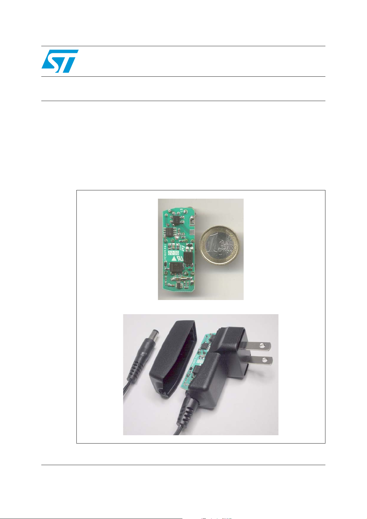
EVALTSM1052: Ultra small battery charger using TSM1052
Introduction
This document describes a low power adapter that can be used in travel battery charger
applications. It uses the new Constant Voltage Constant Current (CVCC) controller
TSM1052, which is housed in one of the smallest packages available (SOT23-6L). Thanks
to its low consumption and low operating voltage, good electrical performance is achieved.
Another important feature of this SMPS is the absence of the Y1 safety capacitor between
primary and secondary grounds.
Figure 1. EVALTSM1052 demo board
July 2007 Rev 1 1/21
www.st.com
Page 2

Contents AN2448
Contents
1 Adapter features . . . . . . . . . . . . . . . . . . . . . . . . . . . . . . . . . . . . . . . . . . . . 4
1.1 Main characteristics . . . . . . . . . . . . . . . . . . . . . . . . . . . . . . . . . . . . . . . . . . 4
1.2 Circuit description . . . . . . . . . . . . . . . . . . . . . . . . . . . . . . . . . . . . . . . . . . . . 6
2 Electrical behavior . . . . . . . . . . . . . . . . . . . . . . . . . . . . . . . . . . . . . . . . . . 7
3 Electrical performance . . . . . . . . . . . . . . . . . . . . . . . . . . . . . . . . . . . . . . 12
3.1 Efficiency . . . . . . . . . . . . . . . . . . . . . . . . . . . . . . . . . . . . . . . . . . . . . . . . . 12
3.2 Output characteristics . . . . . . . . . . . . . . . . . . . . . . . . . . . . . . . . . . . . . . . 13
3.3 Hold-up time . . . . . . . . . . . . . . . . . . . . . . . . . . . . . . . . . . . . . . . . . . . . . . . 14
4 Conducted noise measurements (pre-compliance test) . . . . . . . . . . . 16
5 Thermal measurements . . . . . . . . . . . . . . . . . . . . . . . . . . . . . . . . . . . . . 17
6 BOM . . . . . . . . . . . . . . . . . . . . . . . . . . . . . . . . . . . . . . . . . . . . . . . . . . . . . 19
7 PCB layout . . . . . . . . . . . . . . . . . . . . . . . . . . . . . . . . . . . . . . . . . . . . . . . . 20
8 Revision history . . . . . . . . . . . . . . . . . . . . . . . . . . . . . . . . . . . . . . . . . . . 20
2/21
Page 3

AN2448 List of figures
List of figures
Figure 1. EVALTSM1052 demo board. . . . . . . . . . . . . . . . . . . . . . . . . . . . . . . . . . . . . . . . . . . . . . . . . 1
Figure 2. Electrical diagram . . . . . . . . . . . . . . . . . . . . . . . . . . . . . . . . . . . . . . . . . . . . . . . . . . . . . . . . . 5
Figure 3. V
Figure 4. V
Figure 5. Maximum supply voltages . . . . . . . . . . . . . . . . . . . . . . . . . . . . . . . . . . . . . . . . . . . . . . . . . . 9
Figure 6. Minimum supply voltages . . . . . . . . . . . . . . . . . . . . . . . . . . . . . . . . . . . . . . . . . . . . . . . . . . . 9
Figure 7. V
Figure 8. V
Figure 9. V
Figure 10. V
Figure 11. Efficiency vs. output current . . . . . . . . . . . . . . . . . . . . . . . . . . . . . . . . . . . . . . . . . . . . . . . . 13
Figure 12. Output characteristics at 115 V
Figure 13. Power down at 115 V
Figure 14. Power down at 230 V
Figure 15. CE peak measure at 115 V
Figure 16. CE peak measure at 230 V
Figure 17. V
Figure 18. V
Figure 19. THT components placing (top side) . . . . . . . . . . . . . . . . . . . . . . . . . . . . . . . . . . . . . . . . . . 20
Figure 20. SMT components placing (bottom side) and copper tracks. . . . . . . . . . . . . . . . . . . . . . . . 20
= 115 Vrms - 60 Hz . . . . . . . . . . . . . . . . . . . . . . . . . . . . . . . . . . . . . . . . . . . . . . . . . . . . . 7
in
= 230 Vrms - 50 Hz . . . . . . . . . . . . . . . . . . . . . . . . . . . . . . . . . . . . . . . . . . . . . . . . . . . . . 8
in
= 115 Vac - no-load . . . . . . . . . . . . . . . . . . . . . . . . . . . . . . . . . . . . . . . . . . . . . . . . . . . . 10
in
= 230 Vac - no-load . . . . . . . . . . . . . . . . . . . . . . . . . . . . . . . . . . . . . . . . . . . . . . . . . . . . 10
in
= 115 Vac - short circuit . . . . . . . . . . . . . . . . . . . . . . . . . . . . . . . . . . . . . . . . . . . . . . . . . 11
in
= 230 Vac - short circuit . . . . . . . . . . . . . . . . . . . . . . . . . . . . . . . . . . . . . . . . . . . . . . . . . 11
in
with CDC (cable drop compensation) . . . . . . . . . . . . . . 13
- 60 Hz . . . . . . . . . . . . . . . . . . . . . . . . . . . . . . . . . . . . . . . . . . . . . 14
ac
- 50 Hz . . . . . . . . . . . . . . . . . . . . . . . . . . . . . . . . . . . . . . . . . . . . . 15
ac
= 115 Vac - full load - bottom and top sides. . . . . . . . . . . . . . . . . . . . . . . . . . . . . . . . . . 17
in
= 230 Vac - full load - bottom and top sides. . . . . . . . . . . . . . . . . . . . . . . . . . . . . . . . . . 18
in
ac
and full load . . . . . . . . . . . . . . . . . . . . . . . . . . . . . . . . . . . . . 16
ac
and full load . . . . . . . . . . . . . . . . . . . . . . . . . . . . . . . . . . . . . 16
ac
3/21
Page 4

Adapter features AN2448
1 Adapter features
1.1 Main characteristics
● Input:
–V
– f: 45 ~ 66 Hz
● Output:
–5.1Vdc ± 2%
– 600 mA
– Cable drop compensation (0.33 mV/mA)
● No-load:
– Pin below 0.3 W
● Short circuit: protected with nominal current regulation
● PCB type & size:
–CEM-1
– Single side 35 µm
– 48 x 18 mm
● Safety: according to EN60065
● EMI: according to EN55022 - class B
: 90 ~ 264 Vrms
in
4/21
Page 5
AN2448 Adapter features
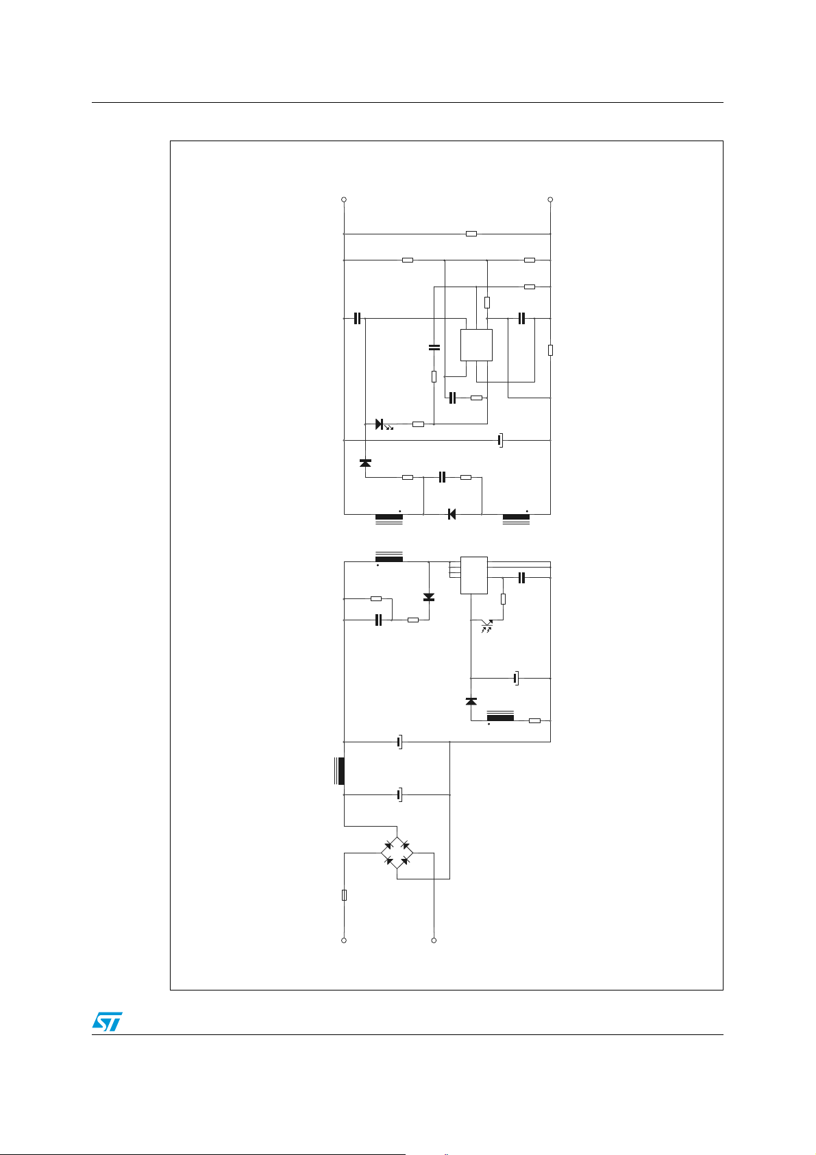
Figure 2. Electrical diagram
Vout
C9
D5
1N4148WS
1uF
IC1B
12
TR1C
EF12.6LP
TR1A
EF12.6LP
21
R1
330K
C4
1.5nF
250V
GND
5.1V - 600mA
R12
2.2K
R9
22K
1%
R7
5
4
6
Vs
C8
R14
SFH617-A3 X007
R6
330 Ohm
R5
100 Ohm
8 6
D2
UF108G
R2
680 Ohm
Vcc
4.7nF
Vctrl1Gnd2Out
IC3
3
22K
R13
220K
C7
22nF
R15
0 Ohm
C11
1.8nF
D4
STPS3L40S
IC2
VIPER12AS-E
8
S
D
7
S
D
6
D
5
D
FB
VDD
4
4
R10
10K
1%
R8
4.7K
C10
10nF
22K 1%
Ictrl
TSM1052
C6
16V
470µF
TR1D
EF12.6LP
1
2
3
R3 1K
3
IC1A
SFH617-A3 X007
C3
33µF
R11
0.33 Ohm
9 7
C5
330nF
50V
D3
1N4148WS
TR1B
EF12.6LP
R4
C2
4.7µF
400V
I1 1mHF1
C1
2.2µF
400V
3
2
10 Ohm 2W
AC1
1
-+
4
D1
S1ZB60
90÷264VAC
AC2
54
2.2 Ohm
5/21
Page 6

Adapter features AN2448
1.2 Circuit description
The circuit used implements a flyback topology, which is ideal for a low power, low cost
isolated converter.
At primary side a VIPer12A-E has been used. This IC includes a current mode PWM
controller and a Power MOSFET in a small SO-8 package. The converter works in both
continuous and discontinuous conduction mode depending on the input voltage (the circuit
has a wide range input) and the output load. The switching frequency is internally fixed at 60
KHz. The design has been developed to reduce overall component count and adapter cost.
The input section includes a resistor for inrush current limiting, a diode bridge, two
electrolytic bulk capacitors and an inductor as front-end ac-dc converter and EMC filter. The
transformer is a layer type, uses a standard EF12.6 ferrite core and is designed to have a
reflected voltage of about 90 V. The peculiarity of this transformer is the winding technique
which allows the elimination of the usual Y1 safety capacitor between the primary and the
secondary. A RCD clamp network is used for leakage inductance demagnetization. The
power supply for the VIPer12A-E is obtained with a self supply winding from the transformer
connected in forward configuration. This circuit provides a voltage that is directly
proportional to the input rectified voltage and independent from the load voltage. In this way
even in short circuit condition (V
operating range (9 V to 38 V) of the VIPer12A-E allows a wide range mains input voltage.
At secondary side, the TSM1052 constant voltage constant current (CVCC) controller is
used. Like the VIPer12A-E, the TSM1052 is also supplied with a forward configuration, in
order to obtain the same benefit. The voltage is taken on one half of the secondary winding
(between pins 8 and 6), rectified with diode D5 and added to the output voltage. Under all
working conditions, the voltage supply for the TSM1052 and the photodiode IC1B is equal to
the output voltage plus forward rectified voltage on half secondary. With this configuration a
correct supply is provided over the whole input range, even with the output short circuited.
= 0), the IC is correctly supplied. The wide VDD
OUT
With this configuration a small ripple at twice line frequency is present at the output. This is
due to the supply of the photodiode IC1B, which is a replica of the voltage on C2. Usually
this is not a problem in battery chargers. There are two ways to eliminate this phenomenon
if necessary:
● C9 can be substituted by an electrolytic capacitor (at least 47 µF)
● The TSM1052 and IC1B can be attached directly to the output voltage. In this case the
current regulation is guaranteed only for output voltages down to 1.7 V
Resistor R7 has been added for cable drop compensation (the higher the output current the
higher the output voltage). R7 has been chosen according to the cable characteristics (it has
about 0.3 Ω of resistance).
6/21
Page 7
AN2448 Electrical behavior
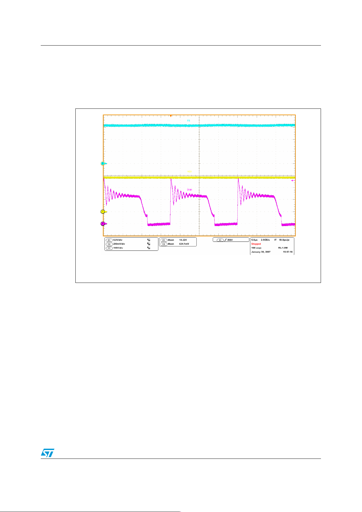
2 Electrical behavior
Figure 3 and Figure 4 show all the VIPer12A-E waveforms during normal operation at full
load. The converter operates in DCM at both 115 Vrms and 230 Vrms:
Figure 3. V
CH1: VIPer12A-E supply voltage (yellow)
CH2: VIPer12A-E feedback pin (red)
CH3: VIPer12A-E drain voltage (green)
= 115 Vrms - 60 Hz
in
7/21
Page 8

Electrical behavior AN2448
Figure 4. Vin = 230 Vrms - 50 Hz
CH1: VIPer12A-E supply voltage (yellow)
CH2: VIPer12A-E feedback pin (light blue)
CH3: VIPer12A-E drain voltage (purple)
Due to the forward supply, the V
is nearly double at 230 V
with respect to 115 Vac.
ac
voltage is directly proportional to the input voltage, so it
DD
The worst case (maximum / minimum) supply voltages for both primary and secondary
sides are shown in Figure 5 and Figure 6.
For the maximum voltages, the converter operates with the maximum load in CV mode (that
is, the maximum output voltage is present, thanks to the cable drop compensation) and with
the maximum input voltage (264 V
). In this condition the VIPer12A-E has a maximum
ac
supply voltage of 35.2 V and the TSM1052 16.16 V. Minimum voltages are taken with short
circuit on the output (CC regulation) and minimum input voltage (90 V
). Given this
ac
condition the VIPer12A-E has a minimum supply voltage of 10.48 V and the TSM1052
2.12 V.
8/21
Page 9

AN2448 Electrical behavior
Figure 5. Maximum supply voltages
CH1: output voltage (yellow)
CH2: VIPer12A-E supply voltage (light blue)
CH3: TSM1052 supply voltage (green)
Figure 6. Minimum supply voltages
CH1: output voltage (yellow)
CH2: VIPer12A-E supply voltage (light blue)
CH3: TSM1052 supply voltage (green)
9/21
Page 10

Electrical behavior AN2448
Let's see what happens at the extreme conditions: no load and short circuit.
During no load conditions, the circuit operates in burst mode allowing an input power of less
than 300 mW over the whole input voltage range.
Figure 7. V
CH1: output voltage (yellow)
CH2: VIPer12A-E drain pin (purple)
CH3: TSM1052 supply voltage (green)
= 115 Vac - no-load
in
Figure 8. V
CH1: output voltage (yellow)
CH2: VIPer12A-E drain pin (purple)
CH3: TSM1052 supply voltage (green)
= 230 Vac - no-load
in
10/21
Page 11

AN2448 Electrical behavior
Figure 9. Vin = 115 Vac - short circuit
CH1: output voltage (yellow)
CH2: VIPer12A-E drain pin (purple)
CH3: TSM1052 supply voltage (green)
Figure 10. V
= 230 Vac - short circuit
in
CH1: output voltage (yellow)
CH2: VIPer12A-E drain pin (purple)
CH3: output current (green)
11/21
Page 12

Electrical performance AN2448
With the circuit used in this evaluation board, when the output current has rapid variation
from maximum to zero and the input voltage is low ( < 105 V
), the VIPer12A-E loses the
ac
supply for about 400-500 ms. The output voltage thereby decreases. After that time the IC
turns on again and the output returns to the nominal value. This behavior is not problematic
in this kind of application and has not been modified, in order to have a smaller and cheaper
solution. If this phenomenon must be avoided, however, it is enough to increase C3 to
100 µF.
3 Electrical performance
3.1 Efficiency
Tab l e 1 and Ta bl e 2 show the board efficiency at the two nominal voltages.
Table 1. Efficiency at 115 Vrms
Io [A] Vo [V] Po [W] Iin [mA] Pin [W] Efficiency
0.1 5.153 0.520 16.9 0.832 62.5%
0.2 5.185 1.036 27.4 1.483 69.9%
0.3 5.217 1.566 38.2 2.235 70.1%
0.4 5.248 2.096 47.6 2.928 71.6%
0.5 5.280 2.638 58.7 3.769 70.0%
0.6 5.310 3.187 68.5 4.530 70.3%
Table 2. Efficiency at 230 Vrms
Io [A] Vo [V] Po [W] Iin [mA] Pin [W] Efficiency
0.1 5.158 0.520 12.8 1.033 50.4%
0.2 5.190 1.037 20.1 1.740 59.6%
0.3 5.222 1.568 25.5 2.364 66.3%
0.4 5.254 2.098 32.6 3.193 65.7%
0.5 5.286 2.641 38.4 3.908 67.6%
0.6 5.319 3.192 43.6 4.572 69.8%
12/21
Page 13

AN2448 Electrical performance
Figure 11. Efficiency vs. output current
Efficiency
75.0%
70.0%
65.0%
60.0%
55.0%
Efficiency
50.0%
45.0%
40.0%
0 0.1 0.2 0.3 0.4 0.5 0.6 0.7
As indicated in Tab l e 3 , the no-load consumption is always below 300 mW, and therefore
complies with the more restrictive standards (European Code Of Conduct).
Table 3. No-load consumption
Val ue 90 V
Pin [W] 0.106 0.131 0.239 0.273
V
[V] 5.12 5.12 5.12 5.12
OUT
ac
3.2 Output characteristics
Figure 12 shows the output characteristics (taken with 115 Vac mains input) on PCB pads
and at the end of the output cable. Values are very close also at 230 V
note that, while in the constant current region, the output voltage can reach zero.
Output current [A]
115V
ac
230V
ac
. It is interesting to
ac
115Vac
230Vac
264V
ac
Figure 12. Output characteristics at 115 V
V-I characteristics
6
5
4
3
2
Outp u t vo ltag e [V ]
1
0
0 200 400 600 800
Output current [mA]
with CDC (cable drop compensation)
ac
PCB output
End of cable
13/21
Page 14

Electrical performance AN2448
The effect of the cable drop compensation is also worthy of note. Tab l e 4 shows the output
voltage at various load amounts measured at the output connector, after the output cable.
115 V
and 230 Vac mains input give very similar results. With the cable drop compensation
ac
the output voltage is nearly constant while, without this feature, at maximum load the output
voltage goes down to 4.96 V (about -3.1%). The effect of this feature is also clearly visible in
the output characteristic (Figure 12), with a flat line while in the constant voltage regulation
region.
Table 4. Output voltage at output connector
Iout [A] 0 0.1 0.2 0.3 0.4 0.5 0.6
Vout [V] with CDC 5.12 5.13 5.13 5.14 5.14 5.15 5.15
Vout [V] without CDC 5.12 5.09 5.07 5.04 5.01 4.98 4.96
3.3 Hold-up time
During power down phase the output voltage undergoes a clean transition without restart
trials or glitches. By observing the waveforms it is possible to measure the hold-up time. In
Figure 13 and Figure 14 this condition is shown for the two nominal voltages of 115 V
230 V
. In the worst case, 115 Vac, a hold-up time of about 17.1 ms is measured.
ac
ac
and
Figure 13. Power down at 115 V
- 60 Hz
ac
CH1: output
voltage (yellow)
CH3: rectified
input voltage
(purple)
14/21
Page 15

AN2448 Electrical performance
Figure 14. Power down at 230 Vac - 50 Hz
CH1: output
voltage (yellow)
CH3: rectified
input voltage
(purple)
15/21
Page 16

Conducted noise measurements (pre-compliance test) AN2448
4 Conducted noise measurements (pre-compliance
test)
Figure 15 and Figure 16 show the conducted noise measurements performed at the two
nominal voltages with peak detection and considering only the worst phase. The
measurements have a good margin with respect to the limits (stated in EN55022 CLASS B
specifications).
Figure 15. CE peak measure at 115 V
Figure 16. CE peak measure at 230 V
and full load
ac
and full load
ac
16/21
Page 17

AN2448 Thermal measurements
5 Thermal measurements
A thermal analysis of the board was performed using an IR camera. The results are shown
in Figure 17 and Figure 18 for 115 V
load condition (Iout = 600 mA).
T
= 25 °C for both figures
AMB
Emissivity = 0.9 for all points
and 230 Vac mains input. Both images refer to full
ac
Figure 17. V
= 115 Vac - full load - bottom and top sides
in
Table 5. Key component temperatures at 115 V
Point Temperature [ºC] Reference
A 69.2 R2 (clamp)
B 72.3 R1 (clamp)
C 63.0 IC2 (VIPer12A-E)
D 66.3 D4 (output diode)
E 68.3 TR1 (windings)
- 600 mA
ac
F 64.0 TR1 (ferrite)
G 66.2 Hot spot on PCB due to bottom side components
17/21
Page 18

Thermal measurements AN2448
Figure 18. Vin = 230 Vac - full load - bottom and top sides
Table 6. Key component temperatures at 230 V
Point Temperature [ºC] Reference
A 70.4 R2 (clamp)
B 72.7 R1 (clamp)
C 67.9 IC2 (VIPer12A-E)
D 66.1 D4 (output diode)
E 70.4 TR1 (windings)
F 66.0 TR1 (ferrite)
G 68.5 Hot spot on PCB due to bottom side components
- 600 mA
ac
18/21
Page 19

AN2448 BOM
6 BOM
Table 7. EVALTSM1052 bill of material
Ref Description Size Manufacturer
C1 Electr.cap. 2.2 µF 400 V 105ºC SEK ø6x11 p2.5 TEAPO/YAGEO
C2 Electr.cap. 4.7 µF 400 V 105ºC SEK ø8x11 p3.5 TEAPO/YAGEO
C3 Electr.cap. 33 µF 50 V 105ºC ø5x11 p2.5
C6 Electr.cap. 470 µF 16 V 105ºC SEK ø8x11 p3.5 TEAPO/YAGEO
C4 Chip capacitor 1.5 nF/250 V X7R 0805
C5 Chip capacitor 330 nF/16 V X7R 0603
C7 Chip capacitor 22 nF/25 V X7R 0603
C8 Chip capacitor 4.7 nF/25 V X7R 0603
C9 Chip capacitor 1 uF/16 V X7R 0603
C10 Chip capacitor 10 nF/50 V X7R 0603
C11 Chip capacitor 1.8 nF/50 V X7R 0603
D1 Single phase bridge S1ZB60 MBS
D2 Diode UF108G D041 PANJIT
D3 D5 DIODE 1N4148WS SOD323
D4 Diode STPS3L40S SMC STMicroelectronics
F1 Fuse res. 10 Ohm ±5% 2 W
I1 Inductor 1 mH CECL-102K COILS ELECTR.
IC1 Opto SFH617-A3 X007 SMT SIEMENS
IC2 I.C. VIPer12AS-E SO8 STMicroelectronics
IC3 I.C. TSM1052CLT SOT23-6L STMicroelectronics
R1 Chip resistor 330 K ±5% 0805
R2 Chip resistor 680 Ohm ±5% 0805
R3 Chip resistor 1 K ±5% 0603
R4 Chip resistor 2.2 Ohm ±5% 0603
R5 Chip resistor 100 Ohm ±5% 0603
R6 Chip resistor 330 Ohm ±5% 0603
R7 R9 Chip resistor 22 K ±1% 0603
R8 Chip resistor 4.7 K ±5% 0603
R10 Chip resistor 10 K ±1% 0603
R11 Chip resistor 0.33 Ohm ±1% 200 ppm 1206
R12 Chip resistor 2.2 K ±5% 0805
R13 Chip resistor 220 K ±5% 0603
19/21
Page 20

PCB layout AN2448
Table 7. EVALTSM1052 bill of material (continued)
Ref Description Size Manufacturer
R14 Chip resistor 22 K ±5% 0603
R15 Chip resistor 0 Ohm 0603
TR1 Transformer EF12.6 LP
7 PCB layout
Figure 19. THT components placing (top side)
Figure 20. SMT components placing (bottom side) and copper tracks
8 Revision history
Table 8. Revision history
Date Revision Changes
04-Jul-2007 1 First issue
20/21
Page 21

AN2448
Please Read Carefully:
Information in this document is provided solely in connection with ST products. STMicroelectronics NV and its subsidiaries (“ST”) reserve the
right to make changes, corrections, modifications or improvements, to this document, and the products and services described herein at any
time, without notice.
All ST products are sold pursuant to ST’s terms and conditions of sale.
Purchasers are solely responsible for the choice, selection and use of the ST products and services described herein, and ST assumes no
liability whatsoever relating to the choice, selection or use of the ST products and services described herein.
No license, express or implied, by estoppel or otherwise, to any intellectual property rights is granted under this document. If any part of this
document refers to any third party products or services it shall not be deemed a license grant by ST for the use of such third party products
or services, or any intellectual property contained therein or considered as a warranty covering the use in any manner whatsoever of such
third party products or services or any intellectual property contained therein.
UNLESS OTHERWISE SET FORTH IN ST’S TERMS AND CONDITIONS OF SALE ST DISCLAIMS ANY EXPRESS OR IMPLIED
WARRANTY WITH RESPECT TO THE USE AND/OR SALE OF ST PRODUCTS INCLUDING WITHOUT LIMITATION IMPLIED
WARRANTIES OF MERCHANTABILITY, FITNESS FOR A PARTICULAR PURPOSE (AND THEIR EQUIVALENTS UNDER THE LAWS
OF ANY JURISDICTION), OR INFRINGEMENT OF ANY PATENT, COPYRIGHT OR OTHER INTELLECTUAL PROPERTY RIGHT.
UNLESS EXPRESSLY APPROVED IN WRITING BY AN AUTHORIZED ST REPRESENTATIVE, ST PRODUCTS ARE NOT
RECOMMENDED, AUTHORIZED OR WARRANTED FOR USE IN MILITARY, AIR CRAFT, SPACE, LIFE SAVING, OR LIFE SUSTAINING
APPLICATIONS, NOR IN PRODUCTS OR SYSTEMS WHERE FAILURE OR MALFUNCTION MAY RESULT IN PERSONAL INJURY,
DEATH, OR SEVERE PROPERTY OR ENVIRONMENTAL DAMAGE. ST PRODUCTS WHICH ARE NOT SPECIFIED AS "AUTOMOTIVE
GRADE" MAY ONLY BE USED IN AUTOMOTIVE APPLICATIONS AT USER’S OWN RISK.
Resale of ST products with provisions different from the statements and/or technical features set forth in this document shall immediately void
any warranty granted by ST for the ST product or service described herein and shall not create or extend in any manner whatsoever, any
liability of ST.
ST and the ST logo are trademarks or registered trademarks of ST in various countries.
Information in this document supersedes and replaces all information previously supplied.
The ST logo is a registered trademark of STMicroelectronics. All other names are the property of their respective owners.
© 2007 STMicroelectronics - All rights reserved
STMicroelectronics group of companies
Australia - Belgium - Brazil - Canada - China - Czech Republic - Finland - France - Germany - Hong Kong - India - Israel - Italy - Japan -
Malaysia - Malta - Morocco - Singapore - Spain - Sweden - Switzerland - United Kingdom - United States of America
www.st.com
21/21
 Loading...