

Page 1

AN2443
Application note
PLC actuator high-side driver solution with CMOS interface
based on VN808CM-E High-side Driver
Main Features
■ 8 output channels (8 x 0.7A)
■ 1 feedback channel - diagnostic
■ CMOS compatible signals allow direct connection to a microcontroller
■ Outputs + Diagnostic indicated by LEDs
■ EMC Immunity Proof ± 4kV level EFT (IEC 61000-4-4 ), ± 2kV Voltage Surge (IEC 6 1000-
4-5)
■ Compatible with existing ST tools (CANIC10, ARMIC30 …)
■ 10.5 ÷ 33V DC Supply Voltage range
Introduction
This application note describes the STEVAL-IFP001V1 hardware implementatio n. It focus
on PCB design which is critical for EMC immunity robustness and thermal management.
The VN808CM-E is a monolithic device designed in STMicroelectronics VIPower M0-3
technology. The product is intended for driving any kind of load with one side connected to
ground. It can be driven b y using a 5.0V or 3.3V log ic supply. Th is allows re alizing an output
stage without optical decoupling or another level-shifting. Active current limitation, combined
with thermal shutdown and automatic restart, protect the device against accidental or longtime short circuit and overload.
The complete solution is implemented on a double-face board with only two copper layers
which is cost-effective, also precision of routing is cost-optimized.
STEVAL-IFP001V1 is delivered in a set with CD-ROM including board fabrication data
(Gerber files), this user manual and related devices documentation (for latest information,
please have a look at www.st.com).
December 2006 Rev 2 1/15
www.st.com
Page 2

Contents AN2443
Contents
1 Overview . . . . . . . . . . . . . . . . . . . . . . . . . . . . . . . . . . . . . . . . . . . . . . . . . . 5
2 Connectors . . . . . . . . . . . . . . . . . . . . . . . . . . . . . . . . . . . . . . . . . . . . . . . . 6
3 Connection description . . . . . . . . . . . . . . . . . . . . . . . . . . . . . . . . . . . . . . 7
4 Thermal management . . . . . . . . . . . . . . . . . . . . . . . . . . . . . . . . . . . . . . . . 9
5 EMC Immunity testing . . . . . . . . . . . . . . . . . . . . . . . . . . . . . . . . . . . . . . . . 9
6 Technical data . . . . . . . . . . . . . . . . . . . . . . . . . . . . . . . . . . . . . . . . . . . . . 10
7 Reference documents . . . . . . . . . . . . . . . . . . . . . . . . . . . . . . . . . . . . . . . 10
Appendix A Bill of materials . . . . . . . . . . . . . . . . . . . . . . . . . . . . . . . . . . . . . . . . . 11
Appendix B PCB layout . . . . . . . . . . . . . . . . . . . . . . . . . . . . . . . . . . . . . . . . . . . . . 12
Revision history . . . . . . . . . . . . . . . . . . . . . . . . . . . . . . . . . . . . . . . . . . . . . . . . . . . . 14
2/15
Page 3

AN2443 List of tables
List of tables
Table 1. Connectors JP1 and JP2 signal assignments . . . . . . . . . . . . . . . . . . . . . . . . . . . . . . . . . . . 6
Table 2. EMC Immunity standards . . . . . . . . . . . . . . . . . . . . . . . . . . . . . . . . . . . . . . . . . . . . . . . . . . . 9
Table 3. STEVAL-IFP001V1 technical data . . . . . . . . . . . . . . . . . . . . . . . . . . . . . . . . . . . . . . . . . . . 10
Table 4. List of components . . . . . . . . . . . . . . . . . . . . . . . . . . . . . . . . . . . . . . . . . . . . . . . . . . . . . . . 11
Table 5. Document revision history . . . . . . . . . . . . . . . . . . . . . . . . . . . . . . . . . . . . . . . . . . . . . . . . . 14
3/15
Page 4

List of figures AN2443
List of figures
Figure 1. STEVAL-IFP001V1 application - top view . . . . . . . . . . . . . . . . . . . . . . . . . . . . . . . . . . . . . . 5
Figure 2. STEVAL-IFP001V1 application - bottom view . . . . . . . . . . . . . . . . . . . . . . . . . . . . . . . . . . . 5
Figure 3. JP1 connector pinout . . . . . . . . . . . . . . . . . . . . . . . . . . . . . . . . . . . . . . . . . . . . . . . . . . . . . . 6
Figure 4. JP2 connector pinout . . . . . . . . . . . . . . . . . . . . . . . . . . . . . . . . . . . . . . . . . . . . . . . . . . . . . . 6
Figure 5. Reverse polarity protection. . . . . . . . . . . . . . . . . . . . . . . . . . . . . . . . . . . . . . . . . . . . . . . . . . 7
Figure 6. Application schematic diagram. . . . . . . . . . . . . . . . . . . . . . . . . . . . . . . . . . . . . . . . . . . . . . . 8
Figure 7. Thermal vias placement suggestion . . . . . . . . . . . . . . . . . . . . . . . . . . . . . . . . . . . . . . . . . . . 9
Figure 8. PCB - top layer . . . . . . . . . . . . . . . . . . . . . . . . . . . . . . . . . . . . . . . . . . . . . . . . . . . . . . . . . . 12
Figure 9. PCB - bottom layer . . . . . . . . . . . . . . . . . . . . . . . . . . . . . . . . . . . . . . . . . . . . . . . . . . . . . . . 12
Figure 10. PCB - silk screen top . . . . . . . . . . . . . . . . . . . . . . . . . . . . . . . . . . . . . . . . . . . . . . . . . . . . . 13
Figure 11. PCB - silk screen bottom . . . . . . . . . . . . . . . . . . . . . . . . . . . . . . . . . . . . . . . . . . . . . . . . . . 13
4/15
Page 5
AN2443 Overview
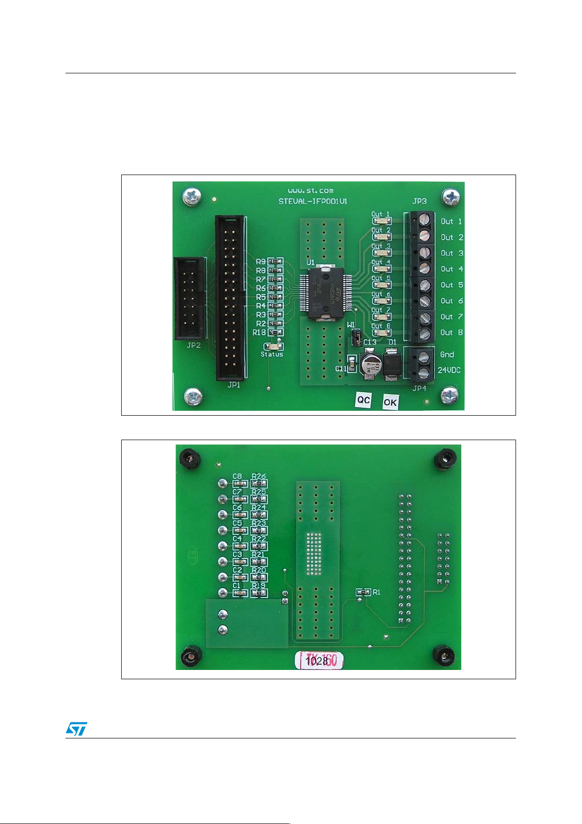
1 Overview
Application is built on double-face, FR4 substrate, printed circuit board with 35µm copper
plating. PCB dimensions are 94 mm x 74 mm.
Figure 1. STEVAL-IFP001V1 application - top view
Figure 2. STEVAL-IFP001V1 application - bottom view
5/15
Page 6

Connectors AN2443
2 Connectors
The application uses two input connectors, one output and one supply voltage terminal.
Both input connectors (JP1 and JP2) pro vide t he sa me signals , the di fference is in type and
pinout. The location of connector JP1 ensures better compatibility with existing tools
(primarily used for motor control).
Figure 3. JP1 connector pinout
Figure 4. JP2 connector pinout
Table 1. Connectors JP1 and JP2 signal assignments
JP1 pin number JP2 pin number Signal Type
2 3 Status Output
4 4 Input 8 Input
10 5 Input 7 Input
14 6 Input 6 Input
20 7 Input 5 Input
22 8 Input 4 Input
23 2 GND Ground - reference
26 9 Input 3 Input
28 10 Input 2 Input
32 11 Input 1 Input
6/15
Page 7

AN2443 Connection description
3 Connection description
The application is connected as shown in Figure 6. It is not intended for a standalone
operation and a control unit is necessary to provide the input signals . The control unit can be
connected either to connector JP1 or JP2. Resistors R1 to R9 protect the control unit and
prevent latch-up. Their value can be extended up to approximately 10kW depending on the
application requirements.
Output states of the VN808CM-E device are monitored by LEDs DS2 to DS9. DS1 is used
for diagnostic purposes. The STATUS pin of the VN808CM-E with its open source structure
provides typically 3mA current in case of o ver-temperature conditions. GND of the device is
typically connected by jumper W1. To ensure the reverse polarity protection, replace this
jumper by a parallel combination of a resistor (e.g. 1kW) and diode (universal or schottky) as
shown in Figure 5.
Output capacitors C1 to C8 improve application EMC immunity robustness, especially for
compliance with standard 61000-4-6 - Immunity to conducted disturbances.
Figure 5. Reverse polarity protection
V
CC
IN1
IN2
IN3
IN4
IN5
IN6
IN7
IN8
STATUS
0V
VN808CM-E
VGND
D1
OUT1
OUT2
OUT3
OUT4
OUT5
OUT6
OUT7
OUT8
R2 (1kΩ)
ai13630
7/15
Page 8
Connection description AN2443
Figure 6. Application schematic diagram
8/15
Page 9

AN2443 Thermal management
4 Thermal management
The PCB includes a 14 x 53mm heatsink on both the top and b ot tom layers. Both heatsinks
are thermally interconnected with vias. Another via grid is placed directly under the device
exposed pad. This grid creates a low-resistive thermal connection of the device thermal slug
to the bottom copper layer. Via drill holes should be approximately 0.3mm in diameter and
the orthogonal grid approximately 1.2mm as shown in Figure 7.
Figure 7. Thermal vias placement suggestion
5 EMC Immunity testing
The application was tested according to electromagnetic compatibility (EMC) immunity
standards IEC61000-4-4 (Fast Transient Burst) and IEC61000-4-5 (High Energy Surge).
The Fast Transient Burst test lasted approximately 1 minute with ±4 kV and a repetition rate
of 5 kHz. All channels were in Switching mode with a frequency of approximately 1Hz. The
burst signal was applied using a capacit ive coupling clamp tool.
The High Energy Surge test was per formed only in Differential mode (no protective GND
available). The signal was coupled by a 42Ω impedance. The test contained five positive
and five negative discharges. The repetition rate was 1 discharge per minute.
The application worked properly during and after the tests. Table 2 shows the test results.
Table 2. EMC Immunity standa rds
Applied to/ Standard IEC61000-4-4 IEC61000-4-5 (Differential Mode)
Supply voltage lines ± 4kV Criteria A ± 2kV Criteria A
Output port ± 4kV Criteria A ± 2kV Criteria A
Application note AN2208 (see Section 7: Reference documents) provides specific
information about test setups.
9/15
Page 10

Technical data AN2443
6 Technical data
Table 3. STEVAL-IFP001V1 technical data
Parameter Min. Typ. Max. Unit
Board Supply Voltage range (recommended) 10.5 33 V DC
Output current per channel (nominal value) 0.5 A DC
Output low level voltage 3 V DC
Supply leakage current @ 24VDC, all inputs grounded 88 µA DC
Input signal low level voltage 0 1.25 V DC
Input signal high level voltage 2.25 6 V DC
1. These values are for information only.
7 Reference documents
[1] AN1351 - VIPower AND BCDmultipower: Making Life Easier with ST’s High-side
Drivers
[2] AN2208 - Designing Industrial Applications with VN808/VN340SP High-side Drivers
(1)
10/15
Page 11

AN2443 Bill of materials
Appendix A Bill of materials
Table 4. List of components
Quantity Ref erence Part Description
Capacitors
8 C1-C8 10nF Ceramic capacitor SMD size 0805, 50V
1 C11 100nF Ceramic capacitor SMD size 0805, 50V
1 C13 22uF Electrolytic capacitor 22uF/50V, SMD +/-20%
Diodes
1 D1 SM15T33A Transil diode, 33V
9 DS1-DS9 LED 1206 LED SMD size 1206, green color
Mechanical parts
1 JP1 MLW34G 34-pin header - dual in line with lock 2.54x2.54mm pitch
1 JP2 MLW14G 14-pin header - dual in line with lock 2.54x2.54mm pitch
4 JP3 ARK508 – 2P 4 x terminal block 5.08mm pitch
1 JP4 ARK508 – 2P 1 x terminal block 5.08mm pitch
1 W1 Jumper 2-pin header 2.54mm pitch
Resistors
9 R1-R9 470R Resistor, SMD size 0805, 150V/300V, 0.125W, 5%
1 R18 1k5 Resistor, SMD size 0805, 150V/300V, 0.125W, 5%
8 R19-R26 4k7 Resistor, SMD size 0805, 150V/300V, 0.125W, 5%
ICs
1 U1 VN808CM-E STMicroelectronics, VN808CM-E, Octal high side driver
11/15
Page 12

PCB layout AN2443
Appendix B PCB layout
Figure 8. PCB - top layer
Figure 9. PCB - bottom layer
12/15
Page 13

AN2443 PCB layout
Figure 10. PCB - silk screen top
Figure 11. PCB - silk screen bottom
13/15
Page 14

Revision history AN2443
Revision history
Table 5. Document revision history
Date Revision Changes
05-Dec-2006 1 Initial release.
14-Dec-2006 2 Figure 5: Reverse polarity protection updated.
14/15
Page 15

AN2443
Please Read Carefully:
Information in this document is provided solely in connection with ST products. STMicroelectronics NV and its subsidiaries (“ST”) reserve the
right to make changes, corrections, modifications or improvements, to this document, and the products and services described herein at any
time, without notice.
All ST products are sold pursuant to ST’s terms and conditions of sale.
Purchasers are solely res ponsibl e fo r the c hoic e, se lecti on an d use o f the S T prod ucts and s ervi ces d escr ibed he rein , and ST as sumes no
liability whatsoever relati ng to the choice, selection or use of the ST products and services described herein.
No license, express or implied, by estoppel or otherwise, to any intellectual property rights is granted under this document. If any part of this
document refers to any third pa rty p ro duc ts or se rv ices it sh all n ot be deem ed a lice ns e gr ant by ST fo r t he use of su ch thi r d party products
or services, or any intellectua l property c ontained the rein or consi dered as a warr anty coverin g the use in any manner whats oever of suc h
third party products or servi ces or any intellectual propert y contained therein.
UNLESS OTHERWISE SET FORTH IN ST’S TERMS AND CONDITIONS OF SALE ST DISCLAIMS ANY EXPRESS OR IMPLIED
WARRANTY WITH RESPECT TO THE USE AND/OR SALE OF ST PRODUCTS INCLUDING WITHOUT LIMITATION IMPLIED
WARRANTIES OF MERCHANTABILITY, FITNESS FOR A PARTICUL AR PURPOS E (AND THEIR EQUIVALE NTS UNDER THE LAWS
OF ANY JURISDICTION), OR INFRINGEMENT OF ANY PATENT, COPYRIGHT OR OTHER INTELLECTUAL PROPERTY RIGHT.
UNLESS EXPRESSLY APPROVED IN WRITING BY AN AUTHORIZED ST REPRESENTATIVE, ST PRODUCTS ARE NOT
RECOMMENDED, AUTHORIZED OR WARRANTED FOR USE IN MILITARY, AIR CRAFT, SPACE, LIFE SAVING, OR LIFE SUSTAINING
APPLICATIONS, NOR IN PRODUCTS OR SYSTEMS WHERE FAILURE OR MALFUNCTION MAY RESULT IN PERSONAL INJ URY,
DEATH, OR SEVERE PROPERTY OR ENVIRONMENTAL DAMAGE. ST PRODUCTS WHICH ARE NOT SPECIFIED AS "AUTOMOTIVE
GRADE" MAY ONLY BE USED IN AUTOMOTIVE APPLICATIONS AT USER’S OWN RISK.
Resale of ST products with provisions different from the statements and/or technical features set forth in this document shall immediately void
any warranty granted by ST fo r the ST pro duct or serv ice describe d herein and shall not cr eate or exten d in any manne r whatsoever , any
liability of ST.
ST and the ST logo are trademarks or registered trademarks of ST in vari ous countries.
Information in this document su persedes and replaces all information previously supplied.
The ST logo is a registered trademark of STMicroelectronics. All other names are the property of their respective owners.
© 2006 STMicroelectronics - All rights reserved
STMicroelectronics group of compan ie s
Australia - Belgium - Brazil - Canada - China - Czech Republic - Finland - Fran ce - Germany - Hong Kong - India - Israel - Italy - Japan -
Malaysia - Malta - Morocco - Singapore - Spain - Sweden - Switzerland - United Kingdom - United States of America
www.st.com
15/15
 Loading...