

Page 1
1 Introduction
This document describes the reference design of the 25W Switch Mode Power Supply
which is dedicated to industrial or white goods applications. The board accepts wide range
input voltages (90 to 265Vrms) and delivers 2 or 3 output voltages depending on the
version. Two types of power supply are availabl e: negativ e output or positive output voltage.
The actual version depends the way the components are assembled on the secondary side
and on the configuration of jumpers. On the primary side, the PCB and transformer are the
same for both versions. More information is available in Chapter 3. The Switch mode power
supply is based on the VIPer53E. The VIPer53E combines in the same package an
enhanced current mode PWM controller with a high voltage MDMesh Power Mosfet. High
efficiency and low standby consumption are the main characteristics of this board. Such
features, coupled with minimal part requirements and global low cost in addition to, makes it
an ideal solution for powering industrial or consumer equipment, meeting worldwide
standards.
AN2426
Applica t ion note
Auxiliary power supply with
VIPer53EDIP
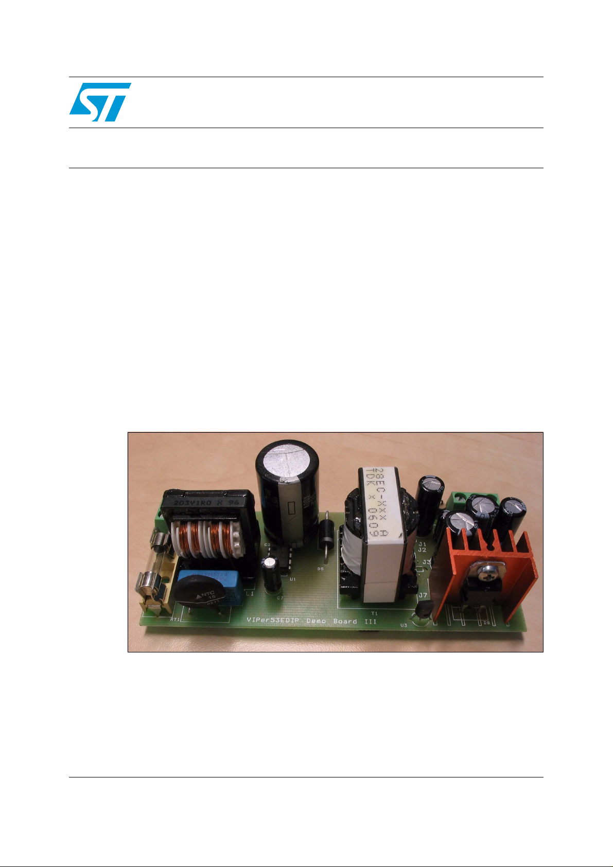
Figure 1. STEVAL-ISA023V1 demo board, described in this application note
January 2007 Rev 1 1/45
www.st.com
Page 2

Contents AN2426 - Application note
Contents
1 Introduction . . . . . . . . . . . . . . . . . . . . . . . . . . . . . . . . . . . . . . . . . . . . . . . . 1
2 Main characteristics . . . . . . . . . . . . . . . . . . . . . . . . . . . . . . . . . . . . . . . . . 6
3 Circuit description . . . . . . . . . . . . . . . . . . . . . . . . . . . . . . . . . . . . . . . . . . . 8
4 Cross regulation and stand by . . . . . . . . . . . . . . . . . . . . . . . . . . . . . . . . 13
5 Functional checking . . . . . . . . . . . . . . . . . . . . . . . . . . . . . . . . . . . . . . . . 16
5.1 Stand by . . . . . . . . . . . . . . . . . . . . . . . . . . . . . . . . . . . . . . . . . . . . . . . . . . 16
5.2 Short-circuit tests . . . . . . . . . . . . . . . . . . . . . . . . . . . . . . . . . . . . . . . . . . . 17
5.3 Start-up behavior at full load . . . . . . . . . . . . . . . . . . . . . . . . . . . . . . . . . . 21
5.4 Wake-up time . . . . . . . . . . . . . . . . . . . . . . . . . . . . . . . . . . . . . . . . . . . . . . 23
5.5 Power down . . . . . . . . . . . . . . . . . . . . . . . . . . . . . . . . . . . . . . . . . . . . . . . 26
5.6 Overvoltage protection . . . . . . . . . . . . . . . . . . . . . . . . . . . . . . . . . . . . . . . 29
5.7 Output ripple voltage at full load . . . . . . . . . . . . . . . . . . . . . . . . . . . . . . . . 29
6 Conducted noise measurements . . . . . . . . . . . . . . . . . . . . . . . . . . . . . . 31
7 Part list . . . . . . . . . . . . . . . . . . . . . . . . . . . . . . . . . . . . . . . . . . . . . . . . . . . 36
8 PCB layout . . . . . . . . . . . . . . . . . . . . . . . . . . . . . . . . . . . . . . . . . . . . . . . . 39
9 Transformer specification . . . . . . . . . . . . . . . . . . . . . . . . . . . . . . . . . . . 41
9.1 Electrical characteristics: . . . . . . . . . . . . . . . . . . . . . . . . . . . . . . . . . . . . . 41
9.2 Manufacturer . . . . . . . . . . . . . . . . . . . . . . . . . . . . . . . . . . . . . . . . . . . . . . 43
10 Revision history . . . . . . . . . . . . . . . . . . . . . . . . . . . . . . . . . . . . . . . . . . . 44
2/45
Page 3

AN2426 - Application note List of tables
List of tables
Table 1. Output voltages , positive version . . . . . . . . . . . . . . . . . . . . . . . . . . . . . . . . . . . . . . . . . . . . . 6
Table 2. Output voltages , negative version . . . . . . . . . . . . . . . . . . . . . . . . . . . . . . . . . . . . . . . . . . . . 6
Table 3. Output voltages at V
Table 4. Output voltages at V
Table 5. Output voltages at V
Table 6. Output voltages at V
Table 7. Output voltages at V
Table 8. Output voltages at V
Table 9. Output voltages at V
Table 10. Output voltages at V
Table 11. Output voltages with open feedback loop - positive version of power supply . . . . . . . . . . . 29
Table 12. Output voltages with open feedback loop - negative version of power supply . . . . . . . . . . 29
Table 13. Bill of material (Part 1 of 3). . . . . . . . . . . . . . . . . . . . . . . . . . . . . . . . . . . . . . . . . . . . . . . . . 36
Table 14. Bill of material (Part 2 of 3). . . . . . . . . . . . . . . . . . . . . . . . . . . . . . . . . . . . . . . . . . . . . . . . . 37
Table 15. Bill of material (Part 3 of 3). . . . . . . . . . . . . . . . . . . . . . . . . . . . . . . . . . . . . . . . . . . . . . . . . 38
Table 16. Winding characteristics of transformer. . . . . . . . . . . . . . . . . . . . . . . . . . . . . . . . . . . . . . . . 43
Table 17. Document revision history . . . . . . . . . . . . . . . . . . . . . . . . . . . . . . . . . . . . . . . . . . . . . . . . . 44
90VAC, 12V / 0.8A. . . . . . . . . . . . . . . . . . . . . . . . . . . . . . . . . . . . . 13
IN
230V A C, 12V / 0 .8A . . . . . . . . . . . . . . . . . . . . . . . . . . . . . . . . . . . . 13
IN
90VAC, 5V / 3A . . . . . . . . . . . . . . . . . . . . . . . . . . . . . . . . . . . . . . . 14
IN
230VAC, 5V / 3A . . . . . . . . . . . . . . . . . . . . . . . . . . . . . . . . . . . . . . 14
IN
90VAC, –12V / 0.8A. . . . . . . . . . . . . . . . . . . . . . . . . . . . . . . . . . . . 14
IN
230VAC, –12V / 0.8A. . . . . . . . . . . . . . . . . . . . . . . . . . . . . . . . . . . 14
IN
90VAC, –5V / 3A . . . . . . . . . . . . . . . . . . . . . . . . . . . . . . . . . . . . . . 15
IN
230V A C, –5V / 3 A . . . . . . . . . . . . . . . . . . . . . . . . . . . . . . . . . . . . . 15
IN
3/45
Page 4

List of figures AN2426 - Application note
List of figures
Figure 1. STEVAL-ISA023V1 demo board, described in this application note . . . . . . . . . . . . . . . . . . 1
Figure 2. Electrical diagram. . . . . . . . . . . . . . . . . . . . . . . . . . . . . . . . . . . . . . . . . . . . . . . . . . . . . . . . . 7
Figure 3. Drain voltage and current at V
Figure 4. Drain voltage and current at V
Figure 5. Drain voltage and current at V
Figure 6. Diodes voltages at V
Figure 7. Drain-source and V
Figure 8. Drain-source and V
= 265VAC - 50Hz and full load. . . . . . . . . . . . . . . . . . . . . . . . . . . . 11
IN
voltage and current at VIN = 90VAC - 50Hz and full load . . . . . . . 12
DD
voltage and current at VIN = 265VAC - 50Hz and full load . . . . . . 12
DD
Figure 9. Power consumption during stand by . . . . . . . . . . . . . . . . . . . . . . . . . . . . . . . . . . . . . . . . . 16
Figure 10. Device voltages in stand by operation . . . . . . . . . . . . . . . . . . . . . . . . . . . . . . . . . . . . . . . . 17
Figure 11. Short circuit on 5V at V
Figure 12. Short circuit on 5V at V
Figure 13. Short circuit on 5V at V
Figure 14. Short circuit on 12V at V
Figure 15. Short circuit on 12V at V
Figure 16. Short circuit on 12V at V
= 90VAC . . . . . . . . . . . . . . . . . . . . . . . . . . . . . . . . . . . . . . . . . . 18
IN
= 230VAC . . . . . . . . . . . . . . . . . . . . . . . . . . . . . . . . . . . . . . . . . 18
IN
= 265VAC . . . . . . . . . . . . . . . . . . . . . . . . . . . . . . . . . . . . . . . . . 19
IN
IN
IN
IN
Figure 17. Start-up, positive version of power supply at V
Figure 18. Start-up, positive version of power supply at V
Figure 19. Start-up, negative version of power supply at V
Figure 20. Start-up, negative version of power supply at V
Figure 21. Wake-up time, positive version of power supply at V
Figure 22. Wake-up time, positive version of power supply at V
Figure 23. Wake-up time, negative version of power supply at V
Figure 24. Wake-up time, negative version of power supply at V
Figure 25. Power down, positive version of power supply at V
Figure 26. Power down, positive version of power supply at V
Figure 27. Power down, negative version of power supply at V
Figure 28. Power down, negative version of power supply at V
Figure 29. Ripple voltage at switching frequency, positive version of power supply . . . . . . . . . . . . . . 30
Figure 30. Ripple voltage at switching frequency, negative version of power supply . . . . . . . . . . . . . 30
Figure 31. Conducted noise measurements Phase A - positive version of power supply,
peak detection . . . . . . . . . . . . . . . . . . . . . . . . . . . . . . . . . . . . . . . . . . . . . . . . . . . . . . . . . . 31
Figure 32. Conducted noise measurements Phase B - positive version of power supply,
peak detection . . . . . . . . . . . . . . . . . . . . . . . . . . . . . . . . . . . . . . . . . . . . . . . . . . . . . . . . . . 32
Figure 33. Conducted noise measurements Phase A - positive version of power supply,
AVG detection. . . . . . . . . . . . . . . . . . . . . . . . . . . . . . . . . . . . . . . . . . . . . . . . . . . . . . . . . . . 32
Figure 34. Conducted noise measurements Phase B - positive version of power supply,
AVG detection. . . . . . . . . . . . . . . . . . . . . . . . . . . . . . . . . . . . . . . . . . . . . . . . . . . . . . . . . . . 33
Figure 35. Conducted noise measurements Phase A - negative version of powe r supply,
peak detection . . . . . . . . . . . . . . . . . . . . . . . . . . . . . . . . . . . . . . . . . . . . . . . . . . . . . . . . . . 33
Figure 36. Conducted noise measurements Phase B - negative version of powe r supply,
peak detection . . . . . . . . . . . . . . . . . . . . . . . . . . . . . . . . . . . . . . . . . . . . . . . . . . . . . . . . . . 34
Figure 37. Conducted noise measurements Phase A - negative version of powe r supply,
AVG detection. . . . . . . . . . . . . . . . . . . . . . . . . . . . . . . . . . . . . . . . . . . . . . . . . . . . . . . . . . . 34
Figure 38. Conducted noise measurements Phase B - negative version of powe r supply,
AVG detection. . . . . . . . . . . . . . . . . . . . . . . . . . . . . . . . . . . . . . . . . . . . . . . . . . . . . . . . . . . 35
Figure 39. Silk screen - top side . . . . . . . . . . . . . . . . . . . . . . . . . . . . . . . . . . . . . . . . . . . . . . . . . . . . . 39
Figure 40. Silk screen - bottom side . . . . . . . . . . . . . . . . . . . . . . . . . . . . . . . . . . . . . . . . . . . . . . . . . . 39
= 90VAC - 50Hz and full load . . . . . . . . . . . . . . . . . . . . . . 9
IN
= 230VAC - 50Hz and full load . . . . . . . . . . . . . . . . . . . . 10
IN
= 265VAC - 50Hz and full load . . . . . . . . . . . . . . . . . . . . 10
IN
= 90VAC . . . . . . . . . . . . . . . . . . . . . . . . . . . . . . . . . . . . . . . . . 19
= 230VAC. . . . . . . . . . . . . . . . . . . . . . . . . . . . . . . . . . . . . . . . . 20
= 265VAC. . . . . . . . . . . . . . . . . . . . . . . . . . . . . . . . . . . . . . . . . 20
= 90VAC . . . . . . . . . . . . . . . . . . . . . . . . 21
IN
= 230V AC . . . . . . . . . . . . . . . . . . . . . . . 22
IN
= 90VAC. . . . . . . . . . . . . . . . . . . . . . . . 22
IN
= 230V AC. . . . . . . . . . . . . . . . . . . . . . . 2 3
IN
= 90VAC. . . . . . . . . . . . . . . . . . . . 24
IN
= 230VA C . . . . . . . . . . . . . . . . . . 24
IN
= 90VAC . . . . . . . . . . . . . . . . . . . 25
IN
= 230VAC . . . . . . . . . . . . . . . . . . 25
IN
= 90VAC. . . . . . . . . . . . . . . . . . . . . 26
IN
= 230VAC . . . . . . . . . . . . . . . . . . . 27
IN
= 90VAC . . . . . . . . . . . . . . . . . . . . 27
IN
= 230VAC . . . . . . . . . . . . . . . . . . . 28
IN
4/45
Page 5

AN2426 - Application note List of figures
Figure 41. Copper tracks - bottom side . . . . . . . . . . . . . . . . . . . . . . . . . . . . . . . . . . . . . . . . . . . . . . . . 40
Figure 42. Transformer layout . . . . . . . . . . . . . . . . . . . . . . . . . . . . . . . . . . . . . . . . . . . . . . . . . . . . . . . 42
Figure 43. Dimension and appearance of transformer . . . . . . . . . . . . . . . . . . . . . . . . . . . . . . . . . . . . 42
Figure 44. Winding position of transformer . . . . . . . . . . . . . . . . . . . . . . . . . . . . . . . . . . . . . . . . . . . . . 43
5/45
Page 6
Main characteristics AN2426 - Application note
2 Main characteristics
The main characteristics of the SMPS are listed below:
● Input voltage: Vin: 90-265Vrms
● Frequency 45-66Hz
● Output voltages are given in Table 1, and 2:
● Standby consumption: <1 Watt
● Short circuit protection: on all outputs with auto-restart at short removal
● EMI according to:EN55022 Class B.
Table 1. Output voltages, positive version
V
OUT
I
OUT
3.3V 100mA 330mW 2%
5V 3A 15W 5%
12V 0.8A 9.6W 15%
P
= 24.93W
OUT
Table 2. Output voltages, negative version
V
OUT
I
OUT
–5V 3A 15W 5%
–12V 0.8A 9.6W 15%
P
= 24.6W
OUT
P
P
MAX
MAX
Stability
Stability
6/45
Page 7
AN2426 - Application note Main characteristics
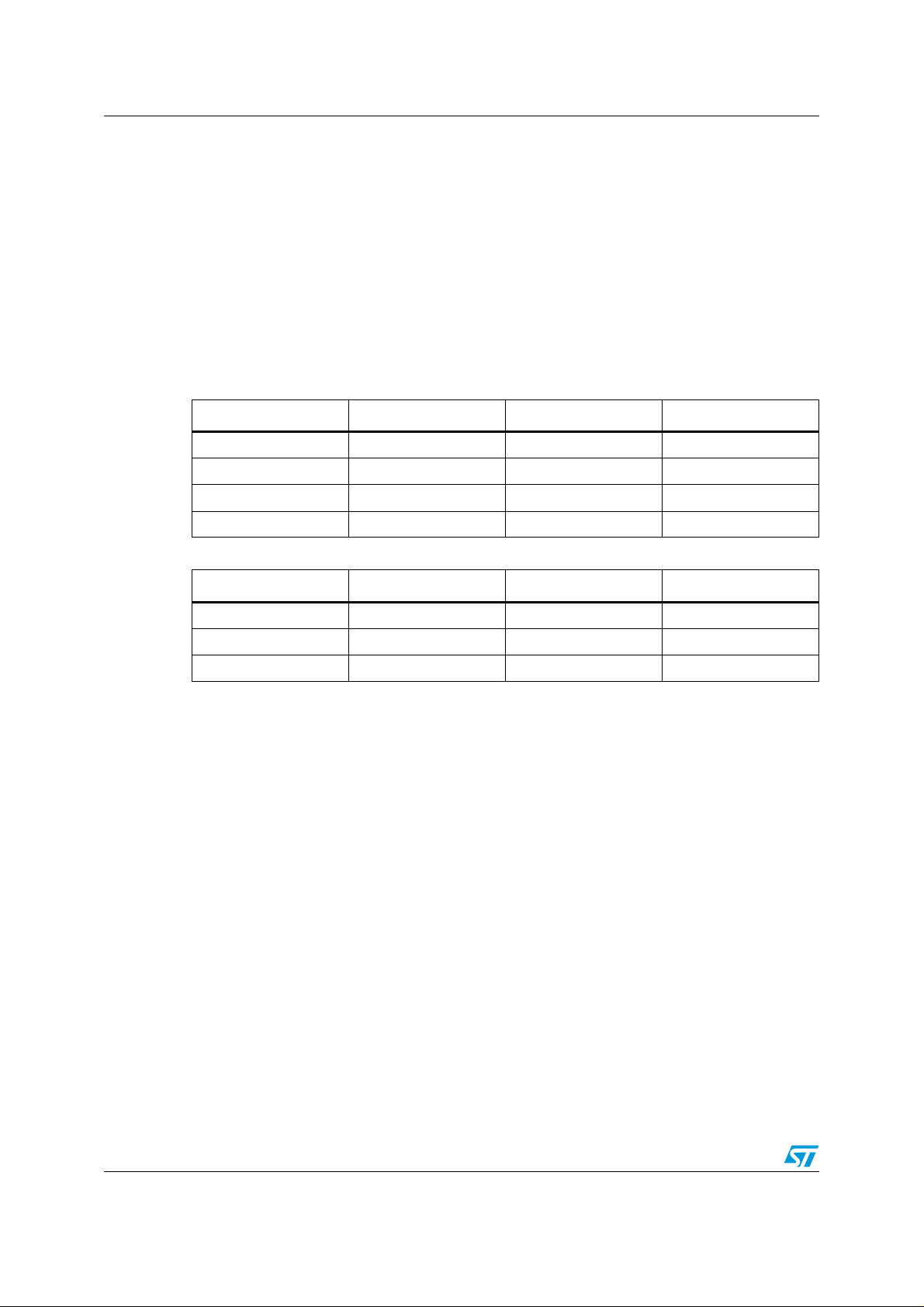
Figure 2. Electrical diagram
CON1
221
100nF/275VAC/X2
100nF/275VAC/X2
R21M
R35.6k
2
6
OSC
V
DD
D
C7
22µF/35V
D2 STPS1150
R5
C8120pF
D3
BAR18
5
1
U1
7
5
15R
F12A
C1
L1
20mH/L11A
C2
-+-+
D1
C368µF/400V
VIPer 53DIP
Q1
BC807-40
D4
STTH1R06
3
4
R11M
D5
RT1
t
1.5KE150A
1
T1
C16
2.2nF/Y1
4.7nF/50V
150nF
39nF
C6
5.1k
Input 85 - 265VAC
C4
NC
C5
8
TOVL
1
COMP
4
R4
S
S
3
7.5k
U2
U2
PC817
R14
1k
470µF/25V
0.1µH
R10
10k
C12
100nF
+
33µF/35V
9.1V
C17
CON2CON2
10
98
D8
STPS2H100
C9
L3
+
C14
D9
Positive version only
Negative version only
AI12637
7
6
3.3µH
470µF/25V
L78L33
D6
0R
L2
STPS1045D
D7
C10
+
1000µF/25V
+
+
C11
1000µF/25V
R7
220R
R9
U3
TL431
R12
R12
15k
+
3
1
C
100nF
C15
120R
U4
V
GND
V
OUT
4
+
R6
220R
R8
0R
R11
R11
15k
+
R13
IN
C18 100n
0
470n
123
43
12
STPS1045D
7/45
Page 8

Circuit description AN2426 - Application note
3 Circuit description
The converter topology of this SMPS is the fly-back, working in continuous and
discontinuous conduction mode. The core of this design is the primary controller
VIPer53EDIP, integrating the controller and a Power Mosfet in a single, standard DIP-8
package. The device integrates all the functions needed to control and protect a power
supply , giving a modern, compact and cheap solution to SMPS designs. If an SMT mounting
is required, a PowerSO-10 version is also available (VIPer53ESP).
The operating frequency of the circuit (~60kHz) has been chosen in order to obtain a
compromise between the transformer size and the input filter complexity. Frequency
modulation has been implemented on the input of VIPer53E to reduce electromagnetic
interferences on the SMPS. Thus, the EMI input filter can be a simple LC-filter consists of
CMC and two X2 capacitors, for differential and common mode noise. The input of SMPS is
protected against inrush peak current by an NTC. In case any catastrophic failures a
standard 5 x 20mm fuse disconnects the SMPS from mains. The transformer reflected
voltage is ~73V, which provides enough room for the leakage inductance voltage spike and
leaves enough margin of reliability. The D4 diode and the D5 transil, clamp the leakage
inductance voltage spike, assuring reliable operation of the Viper53EDIP.
The transformer is manufactured by TDK, and designed according to the safety standard
EN60950. It has two secondary windings, which provide 5 and 12V or –5 and –12V, and an
additional winding which provides the supply voltage for the VIPer53EDIP.
This power supply can generate positive or negative output voltages depending on the
configuration of the jumpers. Jumpers J1, J2, J5 and J7 have to be assembled for the
positive version of the power supply, whilst jumpers J3, J4, J6 and J8 have to be assembled
for the negative version. It is also mandatory to change polarity of the output electrolytic
capacitors: C9, C10, C11, C13 and C14. Diode D6 is found on the secondary side of the
positive power supply, whilst diode D7 is found on the negative side. The polarization of the
diode D8 has to be also changed. The positive power supply can generate a voltage of 3.3V
from the linear regulator U4.
The output rectifiers have been chosen in accordance with the maximum reverse voltage
and their power dissipation. The 5V and –5V rectifier is a Schottky barrier, type
STPS1045D0. It is assembled in an axial TO220 package. The 12V and –12V rectifier is a
Schottky barrier, type STPS2H100. It is assembled in an SMD package. This rectifier has
low forw ard voltage drop, therefore it improves efficiency as it has a lower power dissipation
in comparison with a standard type. A small LC filter has been added on both outputs in
order to filter the high frequency ripple without increasing the output capacitors size or
quality. Output voltage regulation is performed by secondary feedback, which monitors the
5V output. The feedback network is a classical one, which uses a TL431 and optocoupler. I t
assures the required insulation between the primary and secondary sides. The optotransistor drives the COMP pin of the Viper53EDIP, directly. Capacitor C6 and resistor R4
are parts of the compensation loop filtering the high frequency noise.
The VIPer53EDIP is activated at start-up by an internal current source, charging capacitor
C7 from the DC bus via the Drain pin. As a result of this circuit, the start-up time is short and
independent from the mains voltage input. During normal operation the device is powered
by the transformer via the LEB circuit (Q1, C8, D3 and R5) and the D2 diode. The LEB
circuit filters leakage inductance spikes, i.e. it blanks the spike appearing at the leading
edges of the voltage which are generated by the self-supply winding. These spikes, which
are due to inductance leakage from the transformer, are the major cause of raised V
CC
8/45
Page 9
AN2426 - Application note Circuit description
voltages at high load. This circuit also helps to keep the max VCC voltage under control if the
transformer has a high leakage inductance across the auxiliary.
The switching frequency is selected by resistor R3 and capacitor C4. Capacitor C5 provides
a delay to the current protection intervention, the so called TOVL function.
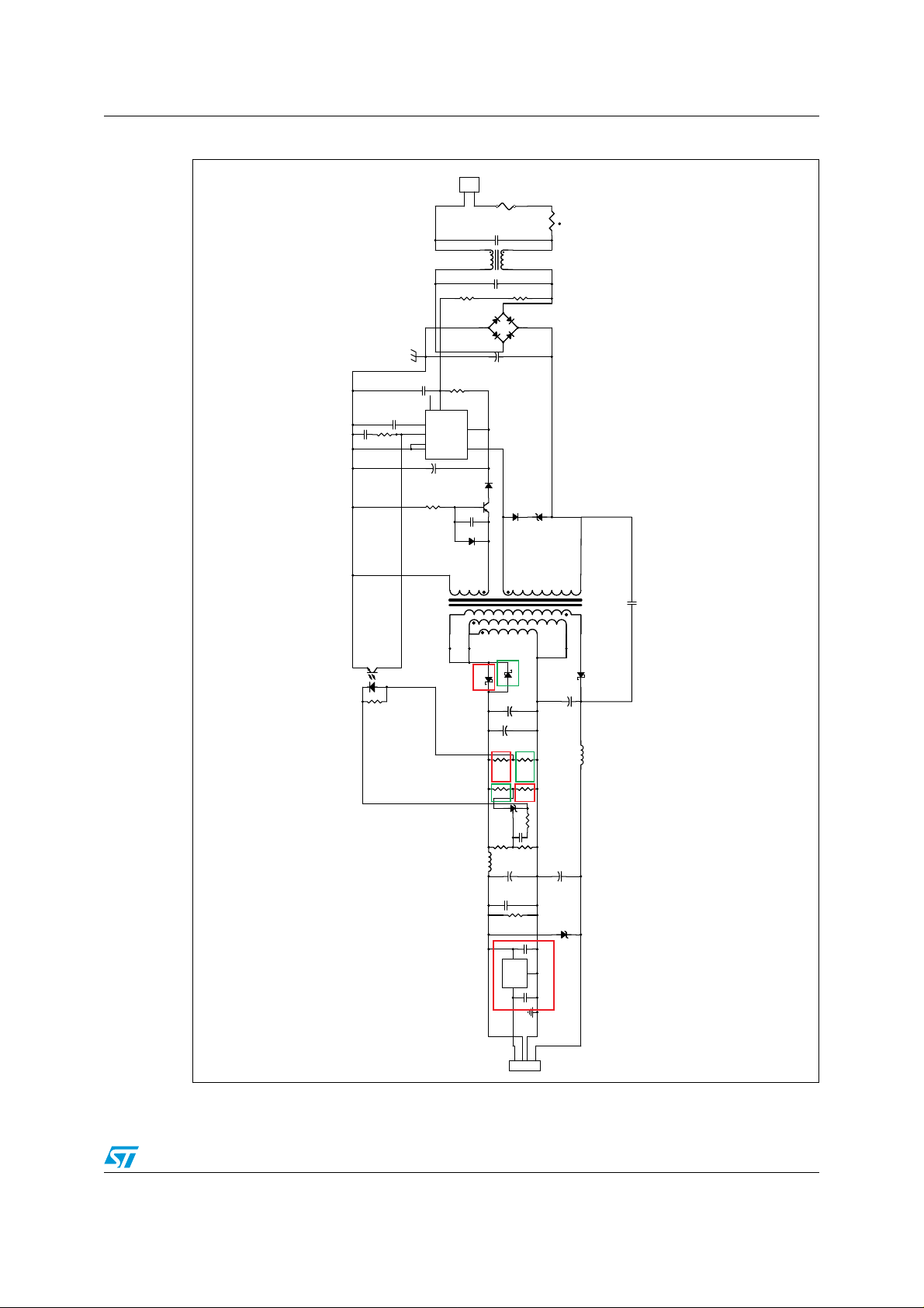
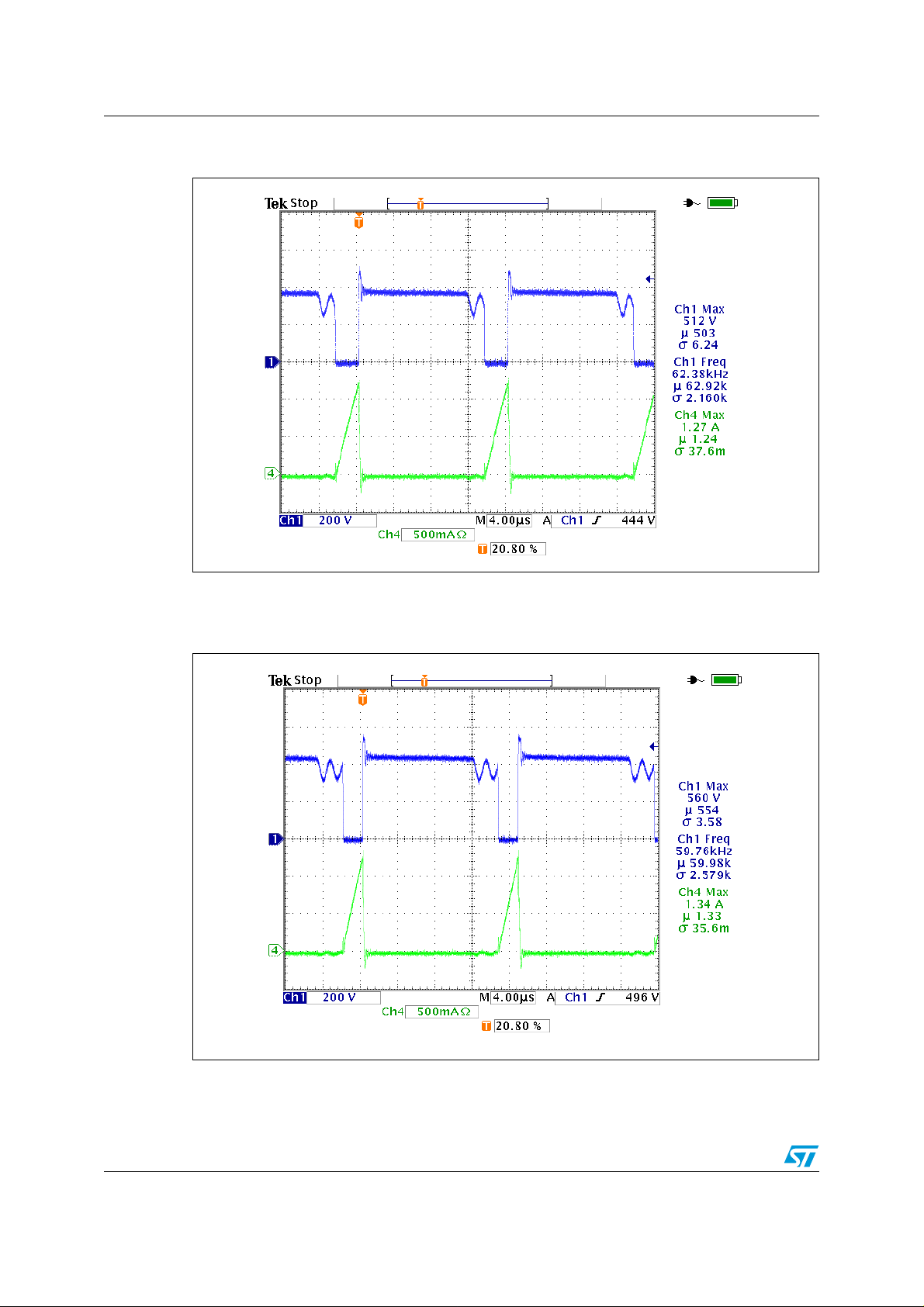
Figure 3, Figure 4 and Figure 5 show the drain voltage and current at nominal mains voltage
input during normal operation at full load. Clearly the current peak is below the maximum
current peak defined in the VIPer53 datasheet. The drain voltage rise time is around 120ns.
Figure 3 shows the drain peak voltage at full load and maximum mains voltage input. The
measured voltage of 564V, assures reliable operation of the Viper53 MOSFET with a good
margin of the maximum break down voltage BV
DSS
(620V).
Figure 3. Drain voltage and current at V
Ch1: VPIN5 (Drain) Ch4: IPIN5 (Drain current)
= 90V AC - 50Hz and full load
IN
9/45
Page 10
Circuit description AN2426 - Application note
Figure 4. Drain voltage and current at VIN = 230VAC - 50Hz and full load
Ch1: VPIN5 (Drain) Ch4: IPIN5 (Drain current)
Figure 5. Drain voltage and current at VIN = 265VAC - 50Hz and full load
Ch1: VPIN5 (Drain) Ch4: IPIN5 (Drain current)
10/45
Page 11
AN2426 - Application note Circuit description
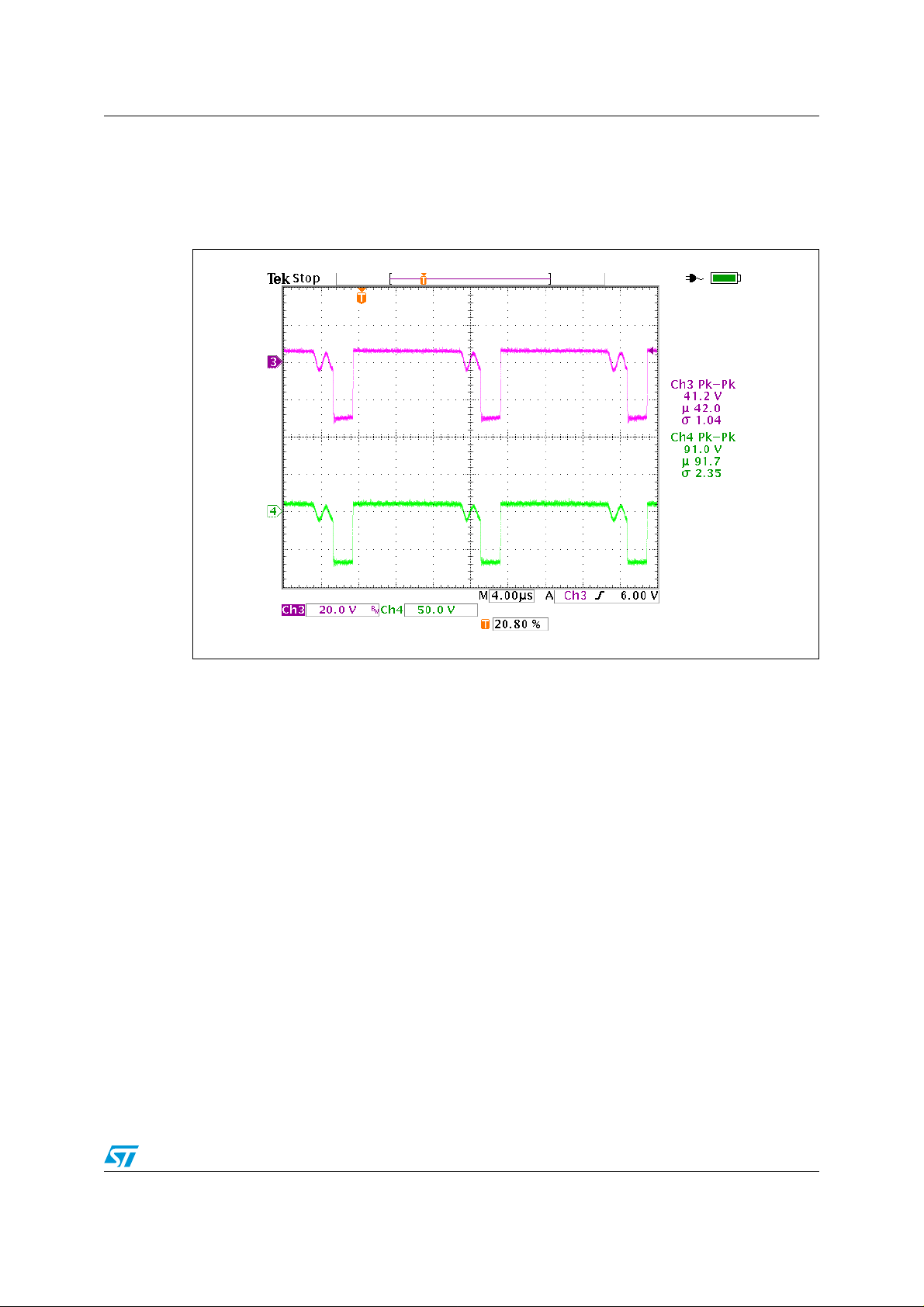
The Figure 6 shows the maximum PIV of rectifiers. They have been measured during 'worst
case scenario'. The margin, with respect to the maximum voltage sustained by each diode,
assure a safe operating conditions for these devices.
Figure 6. Diodes voltages at VIN = 265VAC - 50Hz and full load
Ch3: +5V Diode: Anode voltage Ch4: +12V Diode: Anode voltage
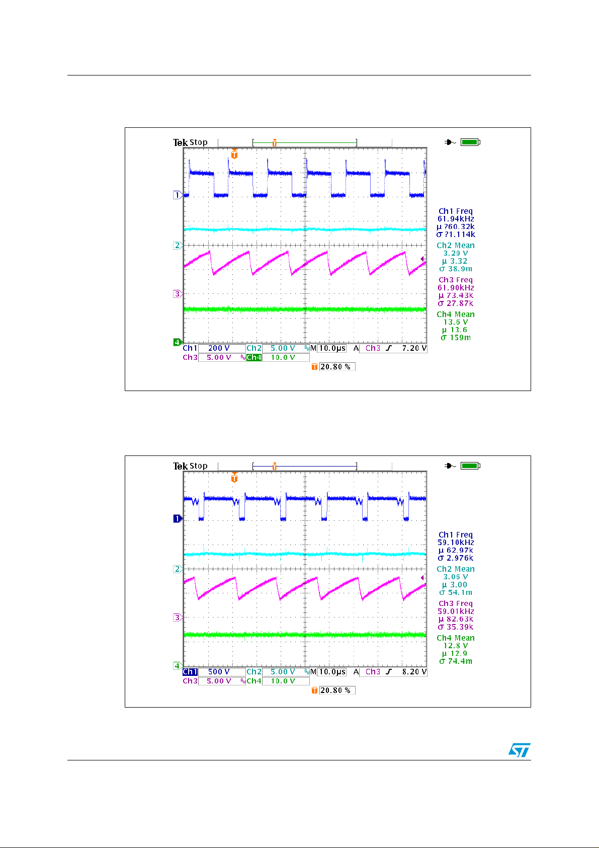
Signals measured on the VIPer53E are shown in Figure 7 and Figure 8, the most salient
controller IC signals are shown. In both figures, clean waveforms, free of hard spikes and
noise that could affect correct operation of SMPS, are distinguishable.
11/45
Page 12
Circuit description AN2426 - Application note
Figure 7. Drain-source and VDD voltage and current at VIN = 90VAC - 50Hz and full
load
Ch1: VPIN5 (Drain) Ch2: VPIN1 (Comp) Ch3: VPIN2 (Osc) Ch4: VPIN7 (V
DD
)
Figure 8. Drain-source and VDD voltage and current at VIN = 265V AC - 50Hz and full
load
Ch1: VPIN5 (Drain) Ch2: VPIN1 (Comp) Ch3: VPIN2 (Osc) Ch4: VPIN7 (V
12/45
DD
)
Page 13
AN2426 - Application note Cross regulation and stand by
4 Cross regulation and stand by
The following tables show the output voltages for both positive and negative version of
power supplies, in addition to the overall efficiency of the converter measured at different
input voltages. All the output voltages have been measured on the output connector. It
should be noted that the 5V output is regulated. The 12V output is influenced by load of 5V
branch. If the 5V voltage branch is not loaded typically the voltage on the 12V branch fall
rapidly down.
Positive version of power supply
Table 3. Output voltages at VIN 90VAC, 12V / 0.8A
3.3V 5V 12V
P
V oltage
[V]
Current
[A]
Voltage
[V]
Current
[A]
Voltage
[V]
Current
[A]
OUT
[W]
3.28 0.1 4.95 0.5 11.00 0.8 11.60 15.30 75.80
3.28 0.1 4.95 1.0 11.13 0.8 14.17 18.70 75.70
3.28 0.1 4.94 1.5 11.23 0.8 16.71 22.00 75.90
P
[W]
IN
Efficiency
[%]
3.28 0.1 4.93 2.0 11.31 0.8 19.22 25.50 75.40
3.28 0.1 4.92 2.5 11.39 0.8 21.73 29.00 74.90
3.28 0.1 4.91 3.0 11.47 0.8 24.23 32.50 74.50
Table 4. Output voltages at VIN 230VAC, 12V / 0.8A
3.3V 5V 12V
Voltage
[V]
Current
[A]
Voltage
[V]
Current
[A]
Voltage
[V]
Current
[A]
P
[W]
OUT
P
[W]
IN
3.28 0.1 4.95 0.5 10.97 0.8 11.58 15.20 76.20
3.28 0.1 4.95 1.0 11.12 0.8 14.16 18.40 76.90
3.28 0.1 4.94 1.5 11.21 0.8 16.70 21.50 77.60
3.28 0.1 4.93 2.0 11.28 0.8 19.20 24.80 77.40
3.28 0.1 4.92 2.5 11.35 0.8 21.70 27.90 77.70
3.28 0.1 4.91 3.0 11.42 0.8 24.19 31.20 77.50
Efficiency
[%]
13/45
Page 14
Cross regulation and stand by AN2426 - Application note
Table 5. Output voltages at VIN 90VAC, 5V / 3A
3.3V 5V 12V
P
Voltage
[V]
Current
[A]
Voltage
[V]
Current
[A]
V oltage
[V]
Current
[A]
OUT
[W]
3.28 0.1 4.91 3.0 12.25 0.2 17.50 23.80 73.50
3.28 0.1 4.91 3.0 11.74 0.4 19.75 26.60 74.20
3.28 0.1 4.91 3.0 11.56 0.6 21.98 29.60 74.20
3.28 0.1 4.91 3.0 11.46 0.8 24.21 32.50 74.50
Table 6. Output voltages at VIN 230VAC, 5V / 3A
3.3V 5V 12V
P
Voltage
[V]
Current
[A]
Voltage
[V]
Current
[A]
Voltage
[V]
Current
[A]
[W]
3.28 0.1 4.91 3.0 12.22 0.2 17.49 23.10 75.70
3.28 0.1 4.91 3.0 11.71 0.4 19.73 25.80 76.50
3.28 0.1 4.91 3.0 11.52 0.6 21.96 28.40 77.30
OUT
P
[W]
P
[W]
IN
IN
Efficiency
[%]
Efficiency
[%]
3.28 0.1 4.91 3.0 11.41 0.8 24.17 31.10 77.70
Negative version of power supply
Table 7. Output voltages at VIN 90VAC, –12V / 0.8A
–5V –12V
Voltage [V] Current [A] Voltage [V] Current [A]
P
OUT
[W]
–4.98 0.5 –10.97 0.8 11.30 14.50 77.70
–4.97 1.0 –11.16 0.8 13.90 18.00 77.20
–4.96 1.5 –11.27 0.8 16.40 21.50 76.50
–4.95 2.0 –11.36 0.8 19.00 25.10 75.60
–4.95 2.5 –11.45 0.8 21.50 28.60 75.20
–4.94 3.0 –11.54 0.8 24.00 32.20 74.60
Table 8. Output voltages at VIN 230VAC, –12V / 0.8A
–5V –12V
Voltage [V] Current [A] Voltage [V] Current [A]
P
OUT
[W]
–4.98 0.5 –10.97 0.8 11.30 14.50 77.70
–4.97 1.0 –11.12 0.8 13.90 17.80 77.90
P
[W]
P
[W]
IN
IN
Efficiency
[%]
Efficiency
[%]
–4.96 1.5 –11.24 0.8 16.40 21.00 78.20
–4.95 2.0 –11.33 0.8 19.00 24.30 78.00
–4.94 2.5 –11.41 0.8 21.50 27.40 78.40
–4.93 3.0 –11.48 0.8 24.00 30.70 78.10
14/45
Page 15

AN2426 - Application note Cross regulation and stand by
Table 9. Output voltages at VIN 90VAC, –5V / 3A
–5V –12V
Voltage [V] Current [A] Voltage [V] Current [A]
P
OUT
[W]
P
IN
[W]
–4.93 3.0 –12.35 0.2 17.30 23.40 73.80
–4.93 3.0 –11.82 0.4 19.50 26.30 74.20
–4.93 3.0 –11.61 0.6 21.70 29.10 74.80
–4.93 3.0 –11.51 0.8 24.00 32.00 75.00
Table 10. Output voltages at VIN 230VAC, –5V / 3A
–5V –12V
Voltage [V] Current [A] Voltage [V] Current [A]
P
OUT
[W]
P
[W]
IN
–4.93 3.0 –12.28 0.2 17.30 22.70 76.00
–4.93 3.0 –11.77 0.4 19.50 25.30 77.00
–4.93 3.0 –11.58 0.6 21.70 28.00 77.60
–4.93 3.0 –11.46 0.8 24.00 30.70 78.00
Efficiency
[%]
Efficiency
[%]
15/45
Page 16

Functional checking AN2426 - Application note
5 Functional checking
5.1 Stand by
The consumption reduction is requested at low load or stand by mode. This request is
completely fulfill thanks burst mode of operation implemented in the VIPer53. When the
VIPer53 detects a light load, it operates automatically in burst mode. VIPer53 monitors the
voltage on pin 1 (Comp) and if this voltage remains lower than 0.5V the device stops
switching cycles. It starts switching cycles again as soon as the voltage on pin 1 increases
to greater than 0.5V. In this way, the output vol tage is always under control and the device is
ready to start. Figure 9 shows power consumptions of positive and negative version of
power supplies during stand-by. Figure 10 shows the main waveforms in stand-by operation.
Figure 9. Power consu m pt i on during stand by
16/45
Page 17

AN2426 - Application note Functional checking
Figure 10. Device voltages in stand by operation
Ch1: VPIN5 (Drain) Ch3: VPIN2 (Osc) Ch2: VPIN1 (Comp) Ch4: VPIN7 (V
5.2 Short-circuit tests
The VIPer53 contains two overload protections. The first one is undervoltage detection on
the V
optocoupler. This protection protects the power supply also against the feedback loop
disconnection. When V
begins to charge. When reaching typically 4 V (V
and the device stops switching. This state is latched thanks to the regulation loop which
maintains the COMP pin voltage above the V
receive any more energy from the auxiliary winding, its voltage drops down until it reaches
V
not reach the V
that the maximum Peak Drain Current value to consider for design purposes is the I
also called Drain Current Capability. The I
trigger overload protection and defines the maximum power output that the power supply
can deliver.
All tests have been performed at minimum, nominal and maximum input voltage. Short
circuit tests have been also made for negative version of power supply and are shown in
Figure 11, Figure 12, Figure13, Figure 14, and Figure 15. Only the most significant positive
power supply images are shown (figures 11 to 15).
When a short occurs the controller enters hiccup mode, and works only for a short period as
shown in figures 11 to 15. This behavior limits the average power dissipation of all devices,
preventing dangerous overheating and catastrophic failure of the SMPS.
pin. The second one depends on the voltage on the COMP pin connected to the
DD
COMP
and the device is reset. If V
DDoff
level, normal operation conditions are resumed. It is important to note
OVLth
)
DD
goes above 4.4 V, the capacitor conn ected on the TOVL pin
), the internal mosfet driver is disabled
OVLth
COMPovl
goes below the OVL threshold till the TOVL pin does
COMP
DMAX
threshold. Since the VDD pin doesn't
DMAX
is the maximum Drain Current that does not
,
17/45
Page 18

Functional checking AN2426 - Application note
Figure 11. Shor t ci rcu it on 5V at VIN = 90VAC
Ch1: VPIN5 (Drain) Ch2: VPIN1 (To vl ) Ch3: VPIN7 (V
Figure 12. Shor t ci rcu it on 5V at VIN = 230VAC
) Ch4: 5V output
DD
Ch1: VPIN5 (Drain) Ch2: VPIN1 (Tovl) Ch3: VPIN7 (V
18/45
) Ch4: 5V output
DD
Page 19

AN2426 - Application note Functional checking
Figure 13. Shor t ci rcu it on 5V at VIN = 265VAC
Ch1: VPIN5 (Drain) Ch2: VPIN1 (To vl) Ch3: VPIN7 (V
Figure 14. Shor t ci rcu it on 12 V at VIN = 90VAC
) Ch4: 5V output
DD
Ch1: VPIN5 (Drain) Ch2: VPIN1 (Tovl) Ch3: VPIN7 (V
19/45
) Ch4: 12V output
DD
Page 20

Functional checking AN2426 - Application note
Figure 15. Shor t ci rcu it on 12 V at VIN = 230VAC
Ch1: VPIN5 (Drain) Ch2: VPIN1 (Tovl) Ch3: VPIN7 (V
Figure 16. Shor t ci rcu it on 12 V at VIN = 265VAC
) Ch4: 12V output
DD
Ch1: VPIN5 (Drain) Ch2: VPIN1 (To vl) Ch3: VPIN7 (V
20/45
) Ch4: 5V output
DD
Page 21

AN2426 - Application note Functional checking
5.3 Start-up behavior at full load
The figures 17, 18, 19 and 20 display the rising slopes of output voltages. The
measurements were perform at full load and for different input voltages (90VAC and
230VAC). As shown in figures 17 to 20, rising time is monotonic and it is almost constant
over all the mains input ranges. No overshoot or abnormal behavior is apparent.
Positive version of power supply
Figure 17. St art-up, positi ve version of power supply at V
= 90VAC
IN
Ch1: VPIN5 (Drain) Ch2: 5V leve l Ch3: 12V level Ch4: 3.3V level
21/45
Page 22

Functional checking AN2426 - Application note
Figure 18. St art-up, positive version of powe r supply at V
= 230VAC
IN
Ch1: VPIN5 (Drain) Ch2: 5V level Ch3: 12V leve l Ch4: 3.3V level
Figure 19. Start-up, negative version of power supply at V
= 90VAC
IN
Ch1: VPIN5 (Drain) Ch2: –5V level Ch3: –12V level
22/45
Page 23

AN2426 - Application note Functional checking
Figure 20. Start-up, negative version of power supply at V
= 230VAC
IN
Ch1: VPIN5 (Drain) Ch2: –5V level Ch3: –12V level
5.4 Wake-up time
The wake-up time is the time needed for the power supply to deliver the nominal output
voltages once it has been plugged-in the mains. During wake up time the external capacitor
on the V
reduced down to I
on the V
Figures 21 to 24 show the wake up time of the power supply. It is clear that no overshoot,
undershoot or loss of control occurs during the power supply wake up time.
pin is charged at about 9mA. When V
DD
DD
rise.
which is about 0.6mA. This lower current leads to a slope change
DDch2
is reached, the charging current is
DDoff
23/45
Page 24

Functional checking AN2426 - Application note
Figure 21. Wake-up time, positive version of power supply at VIN = 90VAC
Ch1: VPIN5 (Drain) Ch2: 5V level Ch3: 12V level Ch4: VPIN7 (V
DD
)
Figure 22. Wake-up time, positive version of power supply at VIN = 230VAC
Ch1: VPIN5 (Drain) Ch2: 5V level Ch3: 12V level Ch4: VPIN7 (V
24/45
DD
)
Page 25

AN2426 - Application note Functional checking
Figure 23. Wake-up time, negative version of power supply at VIN = 90VAC
Ch1: VPIN5 (Drain) Ch2: –5V level Ch3: –12V level Ch4: VPIN7 (V
DD
)
Figure 24. Wake-up tim e, negative ve rsi on of power supply at VIN = 230VAC
Ch1: VPIN5 (Drain) Ch2: –5V level Ch3: –12V level Ch4: VPIN7 (V
25/45
DD
)
Page 26

Functional checking AN2426 - Application note
5.5 Power down
Figures 25 to 28 present the output voltages at converter switch off. All voltages fall at the
same time, because the conv erter doesn't deliver any more energy . However, t he slopes are
individually driven by the output capacitors and the output current.
Figure 25. Power down, positive version of power supply at VIN = 90VAC
Ch1: VPIN5 (Drain) Ch2: VPIN7 (V
) Ch3: 5V level Ch4: 12V level
DD
26/45
Page 27

AN2426 - Application note Functional checking
Figure 26. Power down, positive version of power supply at VIN = 230VAC
Ch1: VPIN5 (Drain) Ch2: VPIN7 (V
) Ch3: 5V level Ch4: 12V level
DD
Figure 27. Power down, n ega ti v e v ers io n of power supply at VIN = 90VAC
Ch1: VPIN5 (Drain) Ch2: VPIN7 (V
27/45
) Ch3: –5V level Ch4: –12V level
DD
Page 28
Functional checking AN2426 - Application note
Figure 28. Power down, n ega ti v e v ers io n of power supply at VIN = 230VAC
Ch1: VPIN5 (Drain) Ch2: VPIN7 (V
) Ch3: –5V level Ch4: –12V level
DD
28/45
Page 29

AN2426 - Application note Functional checking
5.6 Overvoltage protection
The open-loop fault is a very dangerous, event which could happen as a result of feedback
circuitry failure. If this occurs, the SMPS output voltages can rise causing the rectifiers and
output capacitors to be overstressed, destroyed or even catch fire. However, this depends
on the load of each output and the transformer coupling between the windings. The safety
rules requests that the SMPS has to have suitable protection against such risks. The
Viper53 has an integrated overvoltage comparator. The non inverting pin of the overvoltage
comparator is connected to the V
Viper53EDIP stops operations.
The SMPS has been tested with opening the feedback loop. Measured data are shown in
tables 11 and 12.
Table 11. Output voltages with open feedback loop - positive version of power
supply
VIN 230VAC 50Hz Stand by Full load
3.3V 3.30V 3.28V
5.0V 8.29V 5.88V
12.0V 18.18V 13.71V
pin. If the VDD voltage reaches the VDDovp the
DD
Table 12. Output voltages with open feedback loop - negative version of power
supply
V
230VAC 50Hz Stand by Full load
IN
–5.0V –8.47V –6.06V
–12.0V –18.35V –14.22V
5.7 Output ripple voltage at full load
Figures 29 and 30 present the ripple voltage at switching frequency measured at 90V A C on
the input. As shown, ripple voltage spikes are in line with power-supply specifications mainly
thanks LC filters added on the outputs of positive and negative version of power supplies.
29/45
Page 30

Functional checking AN2426 - Application note
Figure 29. Ripple voltage at switching frequency, positive version of power supply
Ch2: 5V level Ch3: 12V level Ch4: 3.3V level
Figure 30. Ripple voltage at switching frequency, negative version of power supply
Ch2–5V level Ch3: –12V level
30/45
Page 31

AN2426 - Application note Conducted noise measurements
6 Conducted noise measurements
The following figures display the conducted noise measurements at full load when a mains
voltage of 230VAC was applied on the inpu t. The measureme nt was made in accordance
with EN55022 CLASS B using Peak and Average detection. The diagrams clearly indicate a
good margin of all measurements with respect to their limits.
Figure 31. Conducted noise measurements Phase A - positive version of power
supply, peak detection
31/45
Page 32

Conducted noise measurements AN2426 - Application note
Figure 32. Conducted noise measurements Phase B - positive version of power
supply, peak detection
Figure 33. Conducted noise measurements Phase A - positive version of power
supply, AVG detection
32/45
Page 33

AN2426 - Application note Conducted noise measurements
Figure 34. Conducted noise measurements Phase B - positive version of power
supply, AVG detection
Figure 35. Conducted noise measurements Phase A - negative version of power
supply, peak detection
33/45
Page 34

Conducted noise measurements AN2426 - Application note
Figure 36. Conducted noise measurements Phase B - negative version of power
supply, peak detection
Figure 37. Conducted noise measurements Phase A - negative version of power
supply, AVG detection
34/45
Page 35

AN2426 - Application note Conducted noise measurements
Figure 38. Conducted noise measurements Phase B - negative version of power
supply, AVG detection
35/45
Page 36

Part list AN2426 - Application note
7 Part list
Table 13. Bill of material (Part 1 of 3)
Item Part Value Description Size Assembly Manufacturer Order code
Version
1 R1 1M/5% Resistor 1206 SMD General
2 R2 1M/5% Resistor 1206 SMD General
3 R3 5k6/5% Resistor 0805 SMD General
4 R4 5k1/5% Resistor 0805 SMD General
5 R5 7k5/5% Resistor 0805 SMD General
6 R6 220R/5% Resistor 0805 SMD General Negative
7 R7 220R/5% Resistor 0805 SMD General Positive
8 R8 0R Resistor 1206 SMD General Positive
9 R9 0R Resistor 0805 SMD General Negative
10 R10 10k/5% Resistor 0805 SMD General
11 R11 15k/5% Resistor 0805 SMD General
12 R12 15k/5% Resistor 0805 SMD General
13 R13 150R Resistor 1206 SMD General
14 R14 1k/5% Resistor 0805 SMD General
15 RT1 15R NTC resistor D15 x 7.5 TH Epcos B57237S0150M
000
16 F1 2A/T Fuse 5 x 20 TH General
17 C1 100nF/275VAC X2 capacitor 18 x 6 TH Epcos B32922A210M
18 C2 100nF/275VAC X2 capacitor 18 x 6 TH Epcos B32922A210M
19 C3 68µF/400V Electrolytic
D18 x 7.5 TH Panasonic EEUED2G680
capacitor
20 C4 4.7nF/50V Ceramic
0805 SMD General
capacitor, X7R
21 C5 39nF/50V Ceramic
0805 SMD General
capacitor, X7R
22 C6 150nF/16V Ceramic
0805 SMD General
capacitor, X7R
23 C7 22µF/35V Electrolytic
D5 x 7.5 TH Jamicon SKR220M1ED11
capacitor
24 C8 120pF/50V Ceramic
0805 SMD General
capacitor, X7R
25 C9 470µF/25V Electrolytic
D8 x 3.5 TH Rubycon 25ZL470M8X20
capacitor
26 C10 1000µF/25V Electrolytic
capacitor
D10 x 5 TH Rubycon 25ZL1000M12.5
X20
36/45
Page 37

AN2426 - Application note Part list
Table 14. Bill of material (Part 2 of 3)
Item Part Value Description Size Assembly Manufactur er Order code
27 C11 1000µF/25V Electrolytic
capacitor
28 C12 100nF/50V Ceramic
capacitor, X7R
29 C13 470µF/25V Electrolytic
capacitor
30 C14 33µF/35V Electrolytic
capacitor
31 C15 100nF/50V Ceramic
capacitor, X7R
32 C16 2.2nF Ceramic
capacitor Y1
33 C17 470nF/16V Ceramic
capacitor, X7R
34 C18 100nF/50V Ceramic
capacitor, X7R
35 L1 20mH/1A CMC coil 24 x 19 TH TDK HF2430-
36 L2 3.3µH/3.8A Inductor D8.5 x 5 TH TDK TSL0808 -
D10 x 5 TH Rubycon 25ZL1000M12.
5X20
0805 SMD General
D8 x 3.5 TH Rubycon 25ZL470M8X20
D5 x 2 TH Rubycon 35ZL33M5X11
0805 SMD General
12 x 10
RM10
0805 SMD General Positive
0805 SMD General Positive
TH Murata DE1E3KX222M
A5B
203Y1R0-T01
3R3M3R8-PF
Version
37 L3 0.1µH/ 1.6A Inductor D4 TH Fastron SMCC-R10M
38 D1 B250C1000SMD Rectified
bridge, 800V,
1A
39 D2 STPS1150 Schottky diode ,
150V, 1A
40 D3 BAR18 Schottky diode ,
80V, 70mA
41 D4 STTH1R06A Ultrafast, 600V, 1ADO214AC SMD ST STTH1R06A
42 D5 1.5KE150A Transil DO201 TH ST 1.5KE150A
43 D6 STPS1045D Schottky di ode ,
45V, 10A
44 D7 STPS1045D Schottky di ode ,
45V, 10A
44 D8 STPS2H100U Schottky di ode,
100V, 2A
45 D9 ZMM9.1V/2% Zener diode SOD80 SMD G eneral
46 U1 VIPer53EDIP PWW controlle r
with MOSFET
47 U2 PC817 Opto coupler SO 4 SMD General
DB-1S SMD General
DO214AC SMD ST STPS1150A
SOT23 SMD ST BAR18
TO220AC TH ST STPS1045D Positive
TO220AC TH ST STPS1045D Negative
SMB SMD ST STPS2H100U
DIP-8 TH ST VIPer53EDIP
37/45
Page 38

Part list AN2426 - Application note
Table 15. Bill of material (Part 3 of 3)
Item Part Value Description Size Assembly Manufacturer Order code
Version
48 U3 TL431 Volt age reference TO 92 TH ST TL1431CZ/CZT/CZ
-AP
49 U4 L78L33 Linear regulator TO92 TH ST L78L33CZ Positiv e
50 Q1 BC807-40 NPN transistor SOT23 SMD ST BC807-40
51 T1 EER28 Transformer TH TDK SRW28EC-
X64V015
52 H1 Heatsink 25 x 23
GM code: V7142B
x16
J1 Jumper Positive
J2 Jumper Positive
J3 Jumper Negative
J4 Jumper Negative
J5 Jumper Positive
J6 Jumper Negative
J7 Jumper Positive
J8 Jumper Negative
38/45
Page 39

AN2426 - Application note PCB layout
8 PCB layout
Figure 39. Silk screen - top side
Figure 40. Silk screen - bottom side
39/45
Page 40

PCB layout AN2426 - Application note
Figure 41. Copper tra cks - bottom si de
40/45
Page 41

AN2426 - Application note Transformer specification
9 Transformer specification
● Application type: Consumer, Home Appliance
● Transformer type: Open
● Coil former: Vertical type 5 + 5 pins
● Maximum temperature rise: 45°C
● Maximum operating ambient temperature: 60°C
● Main insulation: Acc with EN60065.
9.1 Electrical characteristics:
– Converter topology: Flyback, CCM/DCM Mode
– Core type: EER28 - PC40 or equivalent
– Typical operating frequency: 60kHz
– Pr imary inductance: 600µH ±10% at 10kHz - 1V
– Leakage ind uctance: 32µH MAX at 10kHz - 1V
– Maximum peak primary current: 1.4 Apk
– RMS pri ma ry current: 0.45 ARMS.
(a)
(b)
a. Measured between pins 1-3
b. Measured b etween pins 1-3 with all secondary windings shorted.
41/45
Page 42

Transformer specification AN2426 - Application note
Figure 42. Transformer layout
Figure 43. Dimension and appearance of transformer
A: 30.0mm
B: 5.0±0.3mm
C: 4.0±1.0mm
D: 31.5mm
E: 24.0mm
42/45
Page 43

AN2426 - Application note Transformer specification
Table 16. Winding characteristics of transformer
Pins Winding RMS current Number of turns
3-2 Primary -A 0.45A 35
7-8.9 Second ary 1.sect ion 3.92A 6
6-10 Secondary 2.section 2.75A 7
4-5 Auxiliary 0.05A 14
2-1 Primary-B 0.45A 35
Figure 44. Wind in g position o f tra n s form e r
9.2 Manufacturer
TDK Electronics Europe -Germany
Transformer P/N: SRW28EC-X64V015.
43/45
Page 44

Revision history AN2426 - Application note
10 Revision history
Table 17. Document revision history
Date Revision Changes
11-Jan-2007 1 Initial rel ease.
44/45
Page 45

AN2426 - Application note
y
y
Please Read Carefu ll y:
Information in this document is provided solely in connection with ST products. STMicroelectronics NV and its subsidiaries (“ST”) reserve the
right to make changes, corrections, modifications or improvements, to this document, and the products and services described herein at an
time, with out notice.
All ST products are sold pursuant to ST ’ s te rms and condi tions of sale.
Purchase rs are solely respon sible for t he choice, selection a nd use of the ST prod ucts and services d escribed he rei n, and ST assumes no
liability whatsoever relating to the choice, selection or use of the ST products and services described herein.
No license, express or implied, by estoppel or otherwise, to any intellectual property rights is granted under this document. If any part of this
document refers to any third party products or services i t s hall not be deem ed a licen se grant by ST f or the use of such third pa rty product s
or services , or any intel lec tual pro per ty cont aine d ther ein or con sidere d as a warra nty c overi ng th e use i n any mann er w hats oever of such
third party products or s ervices or any i ntellectual property cont ai ned therein.
UNLESS OTHERWISE SET FORTH IN ST’S TERMS AND CONDITIONS OF SALE ST DISCLAIMS ANY EXPRESS OR IMPLIED
WARRANTY WITH RESPECT TO THE USE AND/OR SALE OF ST PRODUCTS INCLUDING WITHOUT LIMITATION IMPLIED
WARRANTIES OF MERCHANTABILITY, FITNESS FOR A PARTICULAR PURPOSE (AND THEIR EQUIVALENTS UNDER THE LAWS
OF ANY JURISD ICTION), OR INFRINGEMENT OF ANY PATENT, COPYRIGHT OR OTHER INTELLECTUAL PROPERTY RIGHT.
UNLESS EXPRESSLY APPROVED IN WRITING BY AN AUTHORIZED ST REPRESENTATIVE, ST PRODUCTS ARE NOT
RECOMM ENDE D, AUTH ORI ZED OR WARR ANT ED FOR U SE IN MIL ITA RY, AIR CR AFT, SPA CE, LIF E SAV ING, OR LI FE S USTA INI NG
APPLICATIONS, NOR IN PRODUCTS OR SYSTEMS WHERE FAILURE OR MALFUNCTION MAY RESULT IN PERSONAL INJURY,
DEATH, OR SEVERE PROPERTY OR ENVIRONMENTAL DAMAGE. ST PR ODUC TS W HIC H ARE NOT SPECIFIED AS "AUTOMOTIVE
GRADE" MAY ONLY BE USED IN AUTOMOTIVE APPLIC A TIONS AT USER’S OWN RISK.
Resale of ST products with provisions different from the statements and/or technical features set forth in this document shall immediately void
any warran ty gr anted by ST fo r the ST produc t or se rvice d es cribed he rein and shall not c reat e o r extend in a ny mann er wha tsoe ver, an
liability of ST.
ST and the ST logo are trademarks or regist ered trademarks of ST in various countri es .
Information in this document supersedes and replaces all information prev i ously supplied.
The ST logo is a registered trademark of STMicroelectronics. All other names are the property of their respective owners.
© 2007 STMi croelectro ni cs - All rights reserved
STMicroelectronics group of com panies
Austra l i a - Be l gi um - Brazil - C anada - China - Cze ch Republic - F i nl and - France - Germany - Hong K ong - India - Isr ael - Italy - Japan -
Malaysi a - M al ta - Morocco - Singapore - Sp ai n - Sweden - Swi tzerland - United Kingdom - United States of Ameri ca
www.st.com
45/45
 Loading...