

Page 1

AN2423
Application note
STMPE2401 - Port expander
keypad controller
Introduction
STMPE2401 is the first in the family of STMicroelectronic’s expander logic products. The
principle of a basic expander logic is the provision of additional I/Os that can be used by the
host processor to implement additional features such as expanding the number of control
signals and mixed signal lines or controlling numerous peripherals.
In addition to the above mentioned basic features, STMPE2401 comes with integrated
intelligence to implement advanced features like Keypad scanning and PWM control. This
application note details the setup and programming of the integrated keypad matrix
controller in STMPE2401.
STMPE2401 can be widely used in the fields of Mobile Communications, Portable media
players, Game console, Mobile Phones, Smart Phones, Consumer Electronics and
computer peripherals like state-of-the-art printers, and Advanced embedded systems.
This application note explains the setup and programming of the integrated keypad matrix
controller in STMPE2401. This document also includes a brief description of the timing
constraints and an example of the programming sequence to illustrate the keypad register
configuration for effective functioning of the Keypad controller.
April 2007 Rev 1 1/22
www.st.com
Page 2

Contents AN2423
Contents
1 Advantages of a STMPE2401 keypad matrix controller . . . . . . . . . . . . . 4
2 Device setup and configuration . . . . . . . . . . . . . . . . . . . . . . . . . . . . . . . . 4
3 Keypad controller . . . . . . . . . . . . . . . . . . . . . . . . . . . . . . . . . . . . . . . . . . . 5
4 Operation modes and clocking . . . . . . . . . . . . . . . . . . . . . . . . . . . . . . . . 8
5 Keypad controller registers . . . . . . . . . . . . . . . . . . . . . . . . . . . . . . . . . . . 9
5.1 Data register . . . . . . . . . . . . . . . . . . . . . . . . . . . . . . . . . . . . . . . . . . . . . . . 12
6 Interrupt registers . . . . . . . . . . . . . . . . . . . . . . . . . . . . . . . . . . . . . . . . . . 14
6.1 Interrupt Control Register (ICR) . . . . . . . . . . . . . . . . . . . . . . . . . . . . . . . . 14
6.2 Interrupt enable mask register (IER) . . . . . . . . . . . . . . . . . . . . . . . . . . . . 14
6.3 Interrupt status register (ISR) . . . . . . . . . . . . . . . . . . . . . . . . . . . . . . . . . . 15
7 Driving and sensing of keypad matrix . . . . . . . . . . . . . . . . . . . . . . . . . 16
7.1 Resistance . . . . . . . . . . . . . . . . . . . . . . . . . . . . . . . . . . . . . . . . . . . . . . . . 17
8 Timing constraints . . . . . . . . . . . . . . . . . . . . . . . . . . . . . . . . . . . . . . . . . 17
8.1 Decoding of multiple keys (keypad matrix) . . . . . . . . . . . . . . . . . . . . . . . . 18
8.2 Ghost key handling . . . . . . . . . . . . . . . . . . . . . . . . . . . . . . . . . . . . . . . . . . 18
8.3 Programming sequence example . . . . . . . . . . . . . . . . . . . . . . . . . . . . . . . 19
8.4 Interrupt servicing . . . . . . . . . . . . . . . . . . . . . . . . . . . . . . . . . . . . . . . . . . . 20
9 Conclusion . . . . . . . . . . . . . . . . . . . . . . . . . . . . . . . . . . . . . . . . . . . . . . . . 20
10 Reference . . . . . . . . . . . . . . . . . . . . . . . . . . . . . . . . . . . . . . . . . . . . . . . . . 21
11 Revision history . . . . . . . . . . . . . . . . . . . . . . . . . . . . . . . . . . . . . . . . . . . 21
2/22
Page 3

AN2423 List of tables
List of tables
Table 1. Valid STMPE2401 slave address . . . . . . . . . . . . . . . . . . . . . . . . . . . . . . . . . . . . . . . . . . . . . 4
Table 2. SYSCON register . . . . . . . . . . . . . . . . . . . . . . . . . . . . . . . . . . . . . . . . . . . . . . . . . . . . . . . . . 8
Table 3. SYSCON description . . . . . . . . . . . . . . . . . . . . . . . . . . . . . . . . . . . . . . . . . . . . . . . . . . . . . . 8
Table 4. Register map for keypad controller module . . . . . . . . . . . . . . . . . . . . . . . . . . . . . . . . . . . . . 9
Table 5. KPC_col register. . . . . . . . . . . . . . . . . . . . . . . . . . . . . . . . . . . . . . . . . . . . . . . . . . . . . . . . . . 9
Table 6. KPC_col description . . . . . . . . . . . . . . . . . . . . . . . . . . . . . . . . . . . . . . . . . . . . . . . . . . . . . . . 9
Table 7. KPC_row_msb register. . . . . . . . . . . . . . . . . . . . . . . . . . . . . . . . . . . . . . . . . . . . . . . . . . . . 10
Table 8. KPC_row_msb description . . . . . . . . . . . . . . . . . . . . . . . . . . . . . . . . . . . . . . . . . . . . . . . . . 10
Table 9. KPC_row_Isb register. . . . . . . . . . . . . . . . . . . . . . . . . . . . . . . . . . . . . . . . . . . . . . . . . . . . . 10
Table 10. KPC_row_Isb description . . . . . . . . . . . . . . . . . . . . . . . . . . . . . . . . . . . . . . . . . . . . . . . . . . 10
Table 11. KPC_ctrl_msb register . . . . . . . . . . . . . . . . . . . . . . . . . . . . . . . . . . . . . . . . . . . . . . . . . . . . 11
Table 12. KPC_ctrl_msb description . . . . . . . . . . . . . . . . . . . . . . . . . . . . . . . . . . . . . . . . . . . . . . . . . 11
Table 13. KPC_ctrl_lsb register . . . . . . . . . . . . . . . . . . . . . . . . . . . . . . . . . . . . . . . . . . . . . . . . . . . . . 11
Table 14. KPC_ctrl_lsb description. . . . . . . . . . . . . . . . . . . . . . . . . . . . . . . . . . . . . . . . . . . . . . . . . . . 12
Table 15. KPC_data_byte0_register. . . . . . . . . . . . . . . . . . . . . . . . . . . . . . . . . . . . . . . . . . . . . . . . . . 12
Table 16. KPC_data_byte0 description . . . . . . . . . . . . . . . . . . . . . . . . . . . . . . . . . . . . . . . . . . . . . . . 12
Table 17. KPC_data_byte1 register . . . . . . . . . . . . . . . . . . . . . . . . . . . . . . . . . . . . . . . . . . . . . . . . . . 12
Table 18. KPC_data_byte1 description . . . . . . . . . . . . . . . . . . . . . . . . . . . . . . . . . . . . . . . . . . . . . . . 13
Table 19. KPC_data_byte2 register . . . . . . . . . . . . . . . . . . . . . . . . . . . . . . . . . . . . . . . . . . . . . . . . . . 13
Table 20. KPC_data_byte2 description . . . . . . . . . . . . . . . . . . . . . . . . . . . . . . . . . . . . . . . . . . . . . . . 13
Table 21. Interrupt control register . . . . . . . . . . . . . . . . . . . . . . . . . . . . . . . . . . . . . . . . . . . . . . . . . . . 14
Table 22. Interrupt control description . . . . . . . . . . . . . . . . . . . . . . . . . . . . . . . . . . . . . . . . . . . . . . . . 14
Table 23. Interrupt enable register . . . . . . . . . . . . . . . . . . . . . . . . . . . . . . . . . . . . . . . . . . . . . . . . . . . 14
Table 24. Interrupt enable description . . . . . . . . . . . . . . . . . . . . . . . . . . . . . . . . . . . . . . . . . . . . . . . . 15
Table 25. Interrupt status register . . . . . . . . . . . . . . . . . . . . . . . . . . . . . . . . . . . . . . . . . . . . . . . . . . . . 15
Table 26. Interrupt status description . . . . . . . . . . . . . . . . . . . . . . . . . . . . . . . . . . . . . . . . . . . . . . . . . 16
Table 27. Revision history . . . . . . . . . . . . . . . . . . . . . . . . . . . . . . . . . . . . . . . . . . . . . . . . . . . . . . . . . 21
3/22
Page 4

Advantages of a STMPE2401 keypad matrix controller AN2423
1 Advantages of a STMPE2401 keypad matrix
controller
● Low CPU utilization (no polling)
● Low power consumption
● Wake-up feature from sleep mode to reduce power consumption
● Simple driver software
● Simple connection to CPU for configuration and communication
● Combinational keys to enhance gaming experience
● Application: mobile phone keypads, all-in-one printers, embedded systems, etc.
2 Device setup and configuration
The device operates at 1.8 V VCC. The clock can be generated through a 32 KHz crystal
connected across XTALIN, XTALOUT pins or through an external clock on XTALIN pin. The
clock frequency for normal operation should not exceed 32 KHz. The Reset pin should be
pulled high for the device to come out of reset and operate in the normal operating mode.
The device can be accessed through the I
can be connected to the same I
2
Philip I
C specification Ver2.1. The slave address is selected by the state of two pins
2
C bus. STMPE2401 supports 7-bit addressing as per the
(GPIO15 and GPIO23). The state of the pins is latched into STMPE2401 at power on and
these address settings are retained until the power is switched off. The slave address can
be changed and latched in again using the soft_reset option in the SYSCON register.
2
The I
C Read/Write is done byte by byte. The R/W bit is added as the LSB to the 7-bit slave
address to make up one byte to be sent through the I
2
C interface and up to four STMPE2401 devices
2
C interface from the Master.
Table 1. Valid STMPE2401 slave address
ADDR1
(GPIO23)
0 0 42h (1000010b) 84h
0 1 43h (1000011b) 86h
1 0 44h (1000100b) 88h
1 1 45h (1000101b) 8Ah
4/22
ADDR0
(GPIO15)
7-bit slave
addressing
8-bit format to be
used (including R/W
bit in LSB)
Page 5
AN2423 Keypad controller
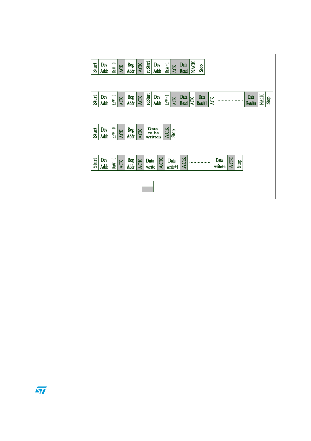
Figure 1. I2C Read/Write protocol
One Byte
Read
Multiple
Byte Read
One Byte
Write
Multiple
Byte Write
Master
Slave
Once the slave address is configured and responds correctly, the internal registers can be
2
accessed through I
C read and write commands.
At power-up all GPIOs function as inputs and by default the interrupt is configured as an
Active Low Level interrupt. The interrupt pin will remain low irrespective of the Interrupt
settings until the Global Interrupt bit (ICR register) is set to '1'.
3 Keypad controller
STMPE2401 comes with an integrated Keypad controller that can control a maximum of
12x8 key matrix. A key press interrupt is generated when a new set of key data is loaded. In
this way, precious CPU resources can be saved by using interrupt servicing instead of
polling.
The main operations of the keypad controller are regulated by four dedicated-key controllers
that support up to four simultaneous dedicated key presses, a key scan controller, and two
normal key controllers. These devices support a maximum of 12x8 key matrix with detection
of two simultaneous key presses.The scanning of each individual row output and column
input can be enabled or masked to support a key matrix of variable size from 1x1 to 12x8.
The first four column inputs can be configured as dedicated keys. If less than 12 columns or
8 rows are used, the rest of the pins can be used for alternate functions like CLKOUT,
Rotator, or GPIO functions.
The operation of the keypad controller is enabled by the SCAN bit of KPC_ctrl register. The
key detection operation always starts with the "any-key" detection whereby the row outputs
are all driven 'LOW' to allow any key press to be sensed.
5/22
Page 6
Keypad controller AN2423
_rd_
Every key activity detected will be de-bounced for a period that can be set through the
KPC_ctrl register before a key press or key release is confirmed and updated into the output
FIFO. The key data, indicating the key coordinates and its status (up or down), is loaded into
the FIFO at the end of a specified number of scanning cycles (set through the
KPC_row_msb register). An interrupt will be generated when a new set of key data is
loaded. The FIFO has a capacity of four sets of key data. Each set of key data consists of
three bytes of information when any of the four dedicated keys is enabled. It is reduced to
two bytes when no dedicated key is enabled. If the FIFO is filled up before its contents are
read, a FIFO overflow interrupt is generated. The FIFO continues to hold its contents but
forbids loading of any new key data until the old data is read.
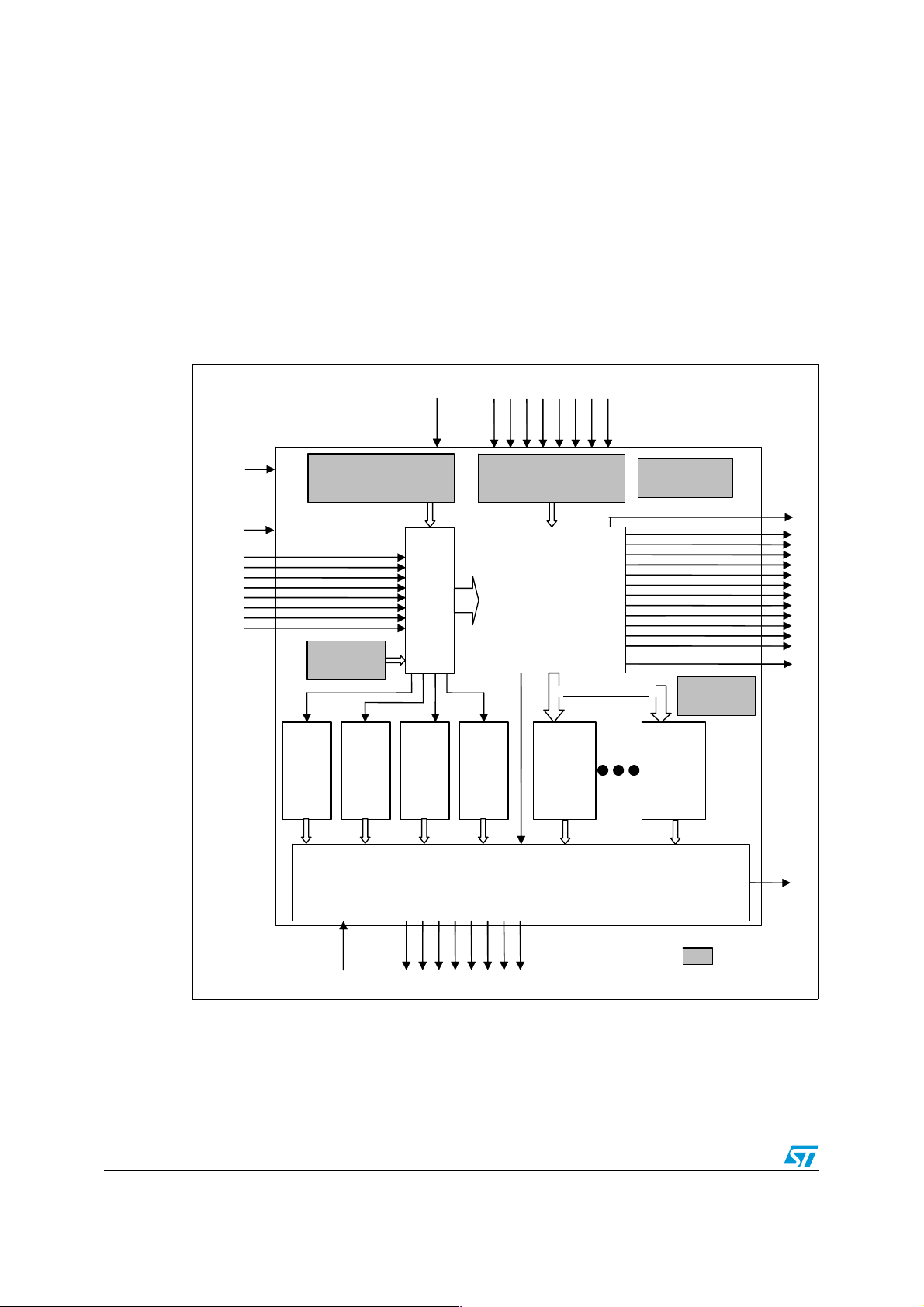
Figure 2. Block diagram of key pad controller
Clk_32KH z
Int_C lk
column_input[7:0]
DKey0~3
(KPC_CTRL)
Dedicated K ey
Controller 0
i2c _w r_ strob e
KPC_COL
Dedicated K ey
Controller 1
i2c_w r_data[7:0]
KPC_ROW
In pu t S e le cto r
Key Scan
Controller
Dedicated K ey
Controller 2
Dedicated K ey
Controller 3
Controller 0
Normal Key
SCAN & HOTKEY
(K PC _ C TR L )
DB_0~7
(K PC _ C TR L )
Normal Key
Controller 2
kpc_wakeup
row_output[1 1:0]
kp c _ in t
strobe i2c_rd_data[7:0]
i2c
The block diagram shows the various inputs to the Keypad Controller block and outputs from
the Keypad controller. The flowchart in Figure 3 describes the Key scan, key press detection
and output FIFO loading operations in the Keypad controller.
6/22
Output Data FIFO
kpc_of
: Control Register
Page 7
AN2423 Keypad controller
N
N
N
N
N
y
N
N
N
p
N
N
N
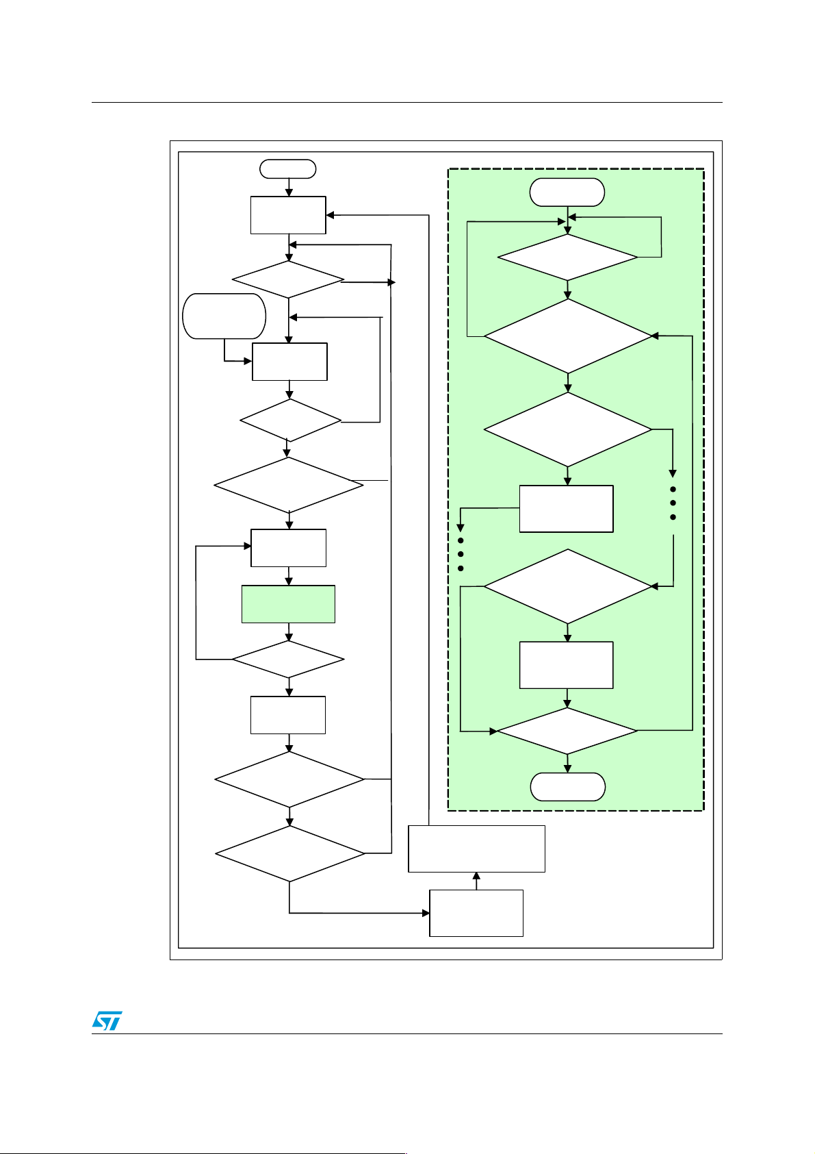
Figure 3. Flowchart of key scan controller operation
T ran sitio n to
sleep m ode
A ny key down?
A ny row output
Y
Reset
Set scan
count = 0
SCAN = ‘1’?
Y
Drive row
outputs
Y
to d riv e?
Y
Drive one
row o ut
C o lu m n in pu t
detection
Next row?
ut
Increm ent
scan count
C o lu m n in p u t
detection
Y
recorded in the de-
de-bounce buffer 1
W rite d ata to d e -
de-bounce buffer 3
W rite d ata to de -
Start
A ny key dow n?
Y
Is the key
bo un ce b uffer
alread
?
Is norm al key
em pty?
Y
bo un ce b uffer 1
Is norm al key
em pty?
Y
b oun ce b uffer 3
A ny m ore key
down?
Y
A ny data ready
for w rite?
End
Y
Scan count =
register setting?
Y
A cknow ledge data w rite
& generate interrupt
W rite ready data
to o u tpu t F IF O
7/22
Page 8

Operation modes and clocking AN2423
4 Operation modes and clocking
The keypad controller can be enabled to run in both operational mode and sleep mode. In
operational mode, the keypad controller runs with an internal clock frequency of 5 MHz
typically. In the sleep mode the clock speed reduces to 32 kHz. However, the interface to I
controller always runs at 5 MHz. The I
2
C interface does not function during sleep mode.
This implies that the keypad function should be configured and enabled before the device
goes into sleep mode.
When the Keypad function is not in use, power consumption can be reduced by disabling the
Keypad Controller. This can be done by setting the 'Enable_KPC' bit in the SYSCON
register to zero.
Table 2. SYSCON register
Bit 7 6 5 4 3 2 1 0
Soft_Reset - Disable_32 KHz Sleep Enable_GPIO Enable_PWM Enable_KPC Enable_ROT
Read/
Write(IIC)
Read/
Write(HW)
Reset
value
WRW RWRWRWRWRW
RW R RW R R R R
00 01111
2
C
Table 3. SYSCON description
Bits Name Description
1 Enable_KPC
4Sleep
5
7
Disable_32 KHz
Soft_Reset
Writing a '0' to this bit gates off the clock to the Keypad Controller module, thus
stopping its operation
Writing a '1' to this bit puts the device in sleep mode. When in sleep mode, all the
units which need to work on clocks synchronous to 32 KHz get the clocks derived
from the 32 K domain. The internal 5 MHz clock is shut down.
Set this bit to '1' to disable the 32 KHz Clk, thus putting the device in hibernate
mode. Only a Reset or a wakeup on I
Writing a '1' to this bit commands a soft reset of the device. Once the reset is
complete, this bit will be cleared to '0' by the HW
2
C restores normal device operation.
In sleep mode, once a key press is sensed and confirmed after de-bounce, a wake-up signal
is generated to activate the internal oscillator (typically 5 MHz). Once the 5 MHz clock is
ready, the I
2
C interface will also be ready for the key data transfer. In the operational mode,
all the de-bounce buffers are reset to no-key condition if a transition to sleep mode occurs.
8/22
Page 9

AN2423 Keypad controller registers
5 Keypad controller registers
There are three control registers and one data register for keypad controllers.
Table 4. Register map for keypad controller module
Auto-Increment
Address Register Name Description
0x60 KPC_col Keypad column scanning register Yes
(during sequential
R/W)
0x61 KPC_row_msb
0x62 KPC_row_lsb Yes
0x63 KPC_ctrl_msb
0x64 KPC_ctrl_lsb Yes
0x68 KPC_data_byte0
0x69 KPC_data_byte1 No
0x6A KPC_data_byte2 No
Keypad row scanning register
Keypad control register
Keypad data register
Ye s
Ye s
No
The key matrix size is configurable through the setting of KPC_row and KPC_col registers
and can be varied from 1x1 to 12x8.
Table 5. KPC_col register
Bit 7 6 5 4 3 2 1 0
Name Input column 0 ~ 7
Read/Write RW RW RW RW RW RW RW RW
Reset value 0 0 0 0 0 0 0 0
Table 6. KPC_col description
Bit Name Description
7 Input column 7 ‘1’ to turn on scanning of column 7; ‘0’ to turn off
6 Input column 6 ‘1’ to turn on scanning of column 6; ‘0’ to turn off
5 Input column 5 ‘1’ to turn on scanning of column 5; ‘0’ to turn off
4 Input column 4 ‘1’ to turn on scanning of column 4; ‘0’ to turn off
3 Input column 3 ‘1’ to turn on scanning of column 3; ‘0’ to turn off
2 Input column 2 ‘1’ to turn on scanning of column 2; ‘0’ to turn off
1 Input column 1 ‘1’ to turn on scanning of column 1; ‘0’ to turn off
0 Input column 0 ‘1’ to turn on scanning of column 0; ‘0’ to turn off
The ScanPW1 and ScanPW0 bits can be adjusted to vary the line rate period (output scan
pulse width setting x internal clock period) for each scan cycle. However, it is recommended
that the default settings '11' be retained to get a typical line rate period of 128 x 200 ns =
25.6 µsec.
9/22
Page 10

Keypad controller registers AN2423
Table 7. KPC_row_msb register
Bit 7 6 543210
Name ScanPW1 ScanPW0 - - Output Row 8 ~ 11
Read/WriteRW RW R R RWRWRWRW
Reset Value1 1 000000
Table 8. KPC_row_msb description
Bit Name Description
7 ScanPW1 Row output scanning pulse width setting:
‘00’: 1x period of internal clock
‘01’: 16x period of internal clock
‘10’: 64x period of internal clock
6ScanPW0
5
--
4
3 Output row 11 ‘1’ to turn on scanning of row 11; ‘0’ to turn off
2 Output row 10 ‘1’ to turn on scanning of row 10; ‘0’ to turn off
‘11’: 128x period of internal clock (default)
(This setting is only applicable during normal
operation mode. The scanning pulse width is 1x
period of 32 kHz clock during sleep mode.)
1 Output row 9 ‘1’ to turn on scanning of row 9; ‘0’ to turn off
0 Output row 8 ‘1’ to turn on scanning of row 8; ‘0’ to turn off
Table 9. KPC_row_Isb register
Bit 7 6 5 43210
Name Output row 0
Read/Write RW RW RW RW RW RW RW RW
Reset value00000000
∼7
Table 10. KPC_row_Isb description
Bit Name Description
7 Output row 7 ‘1’ to turn on scanning of row 7; ‘0’ to turn off
6 Output row 6 ‘1’ to turn on scanning of row 6; ‘0’ to turn off
5 Output row 5 ‘1’ to turn on scanning of row 5; ‘0’ to turn off
4 Output row 4 ‘1’ to turn on scanning of row 4; ‘0’ to turn off
3 Output row 3 ‘1’ to turn on scanning of row 3; ‘0’ to turn off
2 Output row 2 ‘1’ to turn on scanning of row 2; ‘0’ to turn off
1 Output row1 ‘1’ to turn on scanning of row 1; ‘0’ to turn off
0 Output row 0 ‘1’ to turn on scanning of row 0; ‘0’ to turn off
10/22
Page 11

AN2423 Keypad controller registers
Four of the column inputs can be configured as dedicated keys through the setting of
Dkey0~3 bits of KPC_ctrl_msb register. The Scancount0~3 bits determine the number of
scanning cycles performed before loading a set of key-data into the output FIFO. The scan
cycles can be set to maximum to capture multiple key presses in a single interrupt. This
implies that the time between interrupts is longer and a smaller number of interrupts is
serviced as multiple key presses are captured in a single interrupt. A minimum scan cycle
count is useful in cases where very accurate information on the exact key-press sequence is
needed.
Table 11. KPC_ctrl_msb register
Bit 76543210
Name ScanCount0 ~ 3 DKey_0 ~ 3
Read/WriteRWRWRWRWRWRWRWRW
Reset value00000000
Table 12. KPC_ctrl_msb description
Bit Name Description
7 ScanCount3
6 ScanCount2
5 ScanCount1
4 ScanCount0
3 DKey_3 Set ‘1’ to use Input column 3 as dedicated key
Number of key scanning cycles performed before a
confirmed key data is updated into output data FIFO
(0 ~ 15 cycles)
2 DKey_2 Set ‘1’ to use Input column 2 as dedicated key
1 DKey_1 Set ‘1’ to use Input column 1 as dedicated key
0 DKey_0 Set ‘1’ to use Input column 0 as dedicated key
The operation of the keypad controller is enabled by the SCAN bit of KPC_ctrl_lsb register.
Every key activity detected will be de-bounced for a period set by the DB_0~6 bits of
KPC_ctrl_lsb register before a key press or key release is confirmed and updated into the
output FIFO.
Table 13. KPC_ctrl_lsb register
Bit 76543210
Name DB_0 ~ 6 SCAN
Read/Write RW RW RW RW RW RW RW RW
Reset value00000000
11/22
Page 12

Keypad controller registers AN2423
Table 14. KPC_ctrl_lsb description
Bit Name Description
7DB_6
6DB_5
5DB_4
4DB_3
3DB_2
2DB_1
1DB_0
0 SCAN ‘1’ to start scanning; ‘0’ to stop
5.1 Data register
The KPC_DATA register contains three bytes of information. The first two bytes store the key
coordinates and status of any two keys from the normal key matrix, while the third byte
stores the status of dedicated keys.
Table 15. KPC_data_byte0_register
Bit 765 43210
Name Up/DownR3R2 R1R0C2C1C0
Read/WriteR RR RRRRR
Reset value1 11 11000
Table 16. KPC_data_byte0 description
Bit Name Description
0-128 ms of de-bounce time
7 Up/Down ‘0’ for key-down, ‘1’ for key-up
6R3
5R2
4R1
3R0
2C2
0C0
Table 17. KPC_data_byte1 register
Bit 7 6 5 4 3 2 1 0
Name Up/Down R3 R2 R1 R0 C2 C1 C0
Read/Write R R R R R R R R
Reset value 1 1 1 1 1 0 0 0
12/22
row number of key 1 (valid range : 0-11)
0x1111 for No Key
column number of key 1 (valid range : 0-7)1C1
Page 13

AN2423 Keypad controller registers
Table 18. KPC_data_byte1 description
Bit Name Description
7 Up/Down ‘0’ for key-down, ‘1’ for key-up
6R3
5R2
4R1
3R0
2C2
0C0
row number of key 2 (valid range : 0-11)
0x1111 for No Key
column number of key 2 (valid range : 0-7)1C1
Table 19. KPC_data_byte2 register
Bit 76543210
Name Reserved Dedicated key 0 ~ 3
Read/WriteRRRRRRRR
Reset value00001111
Table 20. KPC_data_byte2 description
Bit Name Description
7
6
5
4
3 Dedicated key 3 ‘0’ for key-down, ‘1’ for key-up
2 Dedicated key 2 ‘0’ for key-down, ‘1’ for key-up
1 Dedicated key 1 ‘0’ for key-down, ‘1’ for key-up
0 Dedicated key 0 ‘0’ for key-down, ‘1’ for key-up
Reserved Reserved
13/22
Page 14

Interrupt registers AN2423
6 Interrupt registers
6.1 Interrupt Control Register (ICR)
The ICR is used to configure the Interrupt Controller. It has a global enable interrupt mask
bit (IC0) that controls the interruption to the host. This bit should be set to '1' to enable
interrupts to the host. The type of interrupt and polarity can be set with the IC1 and IC2 bits.
Table 21. Interrupt control register
ICR_lsb [Address 0x11]
Bit 7 6 5 4 3 2 1 0
Reserved IC2 IC1 IC0
R/W R R R R R RW RW RW
Reset
value
00 0 0 0 0 0 0
Table 22. Interrupt control description
Bits Name Description
Global Interrupt Mask bit
0IC[0]
1IC[1]
2IC[2]
When this bit is written with a ‘1’, it will allow interruption to the host. If it is
written with a ‘0’, then, it disables all interruption to the host. Writing to this
bit does not affect the IER value
Output Interrupt Type
‘0’ = Level interrupt
‘1’ = Edge interrup
Output interrupt polarity
'0' = Active low/falling edge
'1' = Active high/rising edge
6.2 Interrupt enable mask register (IER)
IER register should be used to enable the interruption from a particular interrupt source to
the host. For Keypad controller function, the Keypad controller interrupt mask (IE1) and
Keypad Controller FIFO Overflow Interrupt Mask (1E2) bits should be set to '1' to detect
keypad events.
Table 23. Interrupt enable register
IER_msb [Address 0x12] IER_lsb [Address 0x13]
Bit 15141312 11 10 9 8 7 6 5 4 3 2 1 0
Reserved IE8 IE7 IE6 IE5 IE4 IE3 IE2 IE1 IE0
R/W RRRRRR RRW RWRWRWRWRWRWRWRW
Reset
Val ue
14/22
000000 00 0 0 0 0 0 0 0 0
Page 15

AN2423 Interrupt registers
Table 24. Interrupt enable description
Bit Name Description
Interrupt Enable Mask (where x = 8 to 0)
IE0 = Wake-up Interrupt Mask
IE1 = Keypad Controller Interrupt Mask
IE2 = Keypad Controller FIFO Overflow Interrupt Mask
IE3 = Rotator Controller Interrupt Mask
8:0 IE[x]
IE4 = Rotator Controller Buffer Overflow Interrupt Mask
IE5 = PWM Channel 0 interrupt mask
IE6 = PWM Channel 1 interrupt mask
IE7 = PWM Channel 2 interrupt mask
IE8 = GPIO Controller interrupt mask
Writing a ‘1’ to the IE[x] bit enables the interruption to the host.
6.3 Interrupt status register (ISR)
The ISR monitors the status of the interruption from a particular interrupt source to the host.
Regardless of the status of the ER bits (enabled or not), the ISR bits are still updated.
Writing a '1' clears the corresponding interrupt.
Table 25. Interrupt status register
ISR_msb [Address 0x14] ISR_lsb [Address 0x15]
Bit 1514131211109 8 7 6 5 4 3 2 1 0
Reserved IS8 IS7 IS6 IS5 IS4 IS3 IS2 IS1 IS0
R/W R R R R R R R RW RW RW RW RW RW RW RW RW
Reset
Val ue
0000000 0 0 0 0 0 0 0 0 0
15/22
Page 16

Driving and sensing of keypad matrix AN2423
Table 26. Interrupt status description
Bits Name Description
Interrupt status (where x = 8 to 0)
Read:
IS0 = Wake-up interrupt status
IS1 = Keypad controller interrupt status
IS2 = Keypad controller FIFO overflow interrupt status
IS3 = Rotator controller interrupt status
8:0 IS[x]
IS4 = Rotator controller buffer overflow interrupt status
IS5 = PWM Channel 0 interrupt status
IS6 = PWM Channel 1 interrupt status
IS7= PWM Channel 2 interrupt status
IS8 = GPIO Controller interrupt status
Write:
A write to a IS[x] bit with a value of ‘1’ will clear the interrupt and a write
with a value of ‘0’ has no effect on the IS[x] bit
7 Driving and sensing of keypad matrix
The keypad column inputs enabled by the KPC_col register are normally 'HIGH', with the
corresponding input pins pulled up by resistors internally. After reset, all the keypad row
outputs enabled by the KPC_row register are driven 'LOW'. If a key is pressed, its
corresponding column input will become 'LOW' after making contact with the 'LOW' voltage
on its corresponding row output.
Once the key scan controller senses a 'LOW' input on any of the column inputs, the
scanning cycles start to determine the exact key that has been pressed.
If the row output is enabled, the twelve row outputs are driven, 'LOW' one by one during
each scanning cycle. If a row output is not driven 'LOW', it is in tri-state with internal pull-up.
If there is any column input sensed as 'LOW' when a row is driven 'LOW', the key scan
controller:
1. decodes the key coordinates (its corresponding row number and column number),
2. saves the key data into a de-bounce buffer if available,
3. confirms if it is a valid key press after de-bouncing, and
4. updates the key data into output data FIFO if valid.
16/22
Page 17
AN2423 Timing constraints
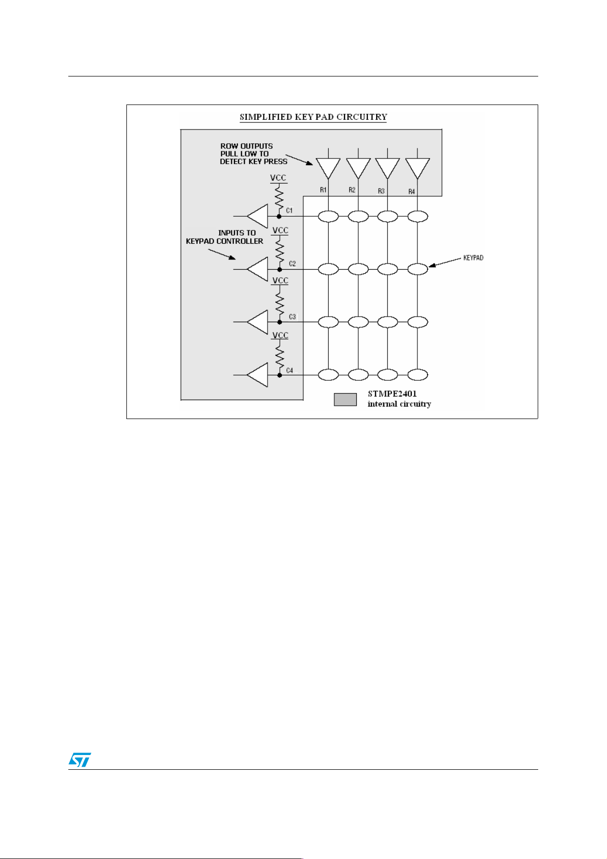
Figure 4. Simplified keypad circuitry
COLUMN
7.1 Resistance
The maximum resistance between the keypad input and keypad output inclusive of switch
resistance, protection circuits and connections should be less than 3.2 Kohms.
8 Timing constraints
The scan rate of the keypad matrix = (Number of rows to be scanned + 1) x Line Rate
period.
Line rate period = Maximum internal Clock period (125 ns typically) x Scanning Pulse Width
Setting (recommended is 128)
= 125 ns x 128 = 16 µsec.
Assuming the maximum number of rows to be scanned is 12, then the complete scan cycle
is:
Single Scan cycle time = (Number of rows + 1) x Line rate period
= 13 x 16
µs = 208 µsec.
17/22
Page 18

Timing constraints AN2423
put
put
Assuming a minimum scan count setting [KPC_ctrl_msb_register] of 1, the interrupt is
generated every 208 µsec.
This assumption implies that for two key presses to be reported in the same interrupt, the
interval between the two key presses (after debouncing) should be less than 208 µsec.
If there is a maximum scan count setting of 16, the maximum duration between interrupts
will be 208 µs x 16 = 3.3 msec.
A key press interrupt is generated when a set of key data is written into the FIFO buffer. The
host must ensure that the interrupt service routine is able to clear the corresponding key
detection interrupt bit in the Interrupt Service Register (ISR) within the above mentioned
time interval in order to not miss any successive interrupt.
No Interrupt is generated until the previously set ISR bit is cleared. It might happen that
before the interrupt is serviced, all four FIFO buffers are filled up due to successive key
press events. In this case, it is recommended that the host continuously read the key data
buffer until it gets an empty key data to ensure all key data are processed promptly
whenever a key detection interrupt occurs. If not, the FIFO overflow interrupt is generated
and no new key data is loaded into the FIFO until all the old key data are read and cleared.
8.1 Decoding of multiple keys (keypad matrix)
The keypad controller is designed for the detection of only two simultaneous normal key
presses from the key matrix. In the case of more than two key presses at the same time,
only two keys will be decoded while the others are ignored. Since the rows are scanned one
by one, the keys on row 0 will be decoded first, followed by row 1 and so on. If multiple key
events happen in the same row, the key in column 0 will be decoded first, followed by
column 1 and so on.
8.2 Ghost key handling
Similar to all matrix keypads without diodes at the keys, the system is vulnerable to a
situation known as "ghost key". Ghost key may occur when more than 2 keys are pressed
and held down at the same time.
Figure 5 shows a situation where ghost key occurs:
Figure 5. Ghost key
Output 1
Output 2
Output 3
Ghost Key
In
1
In
2
Input 3
18/22
Page 19

AN2423 Timing constraints
Three keys are pressed and held down simultaneously. KPC scans the matrix by driving the
outputs to LOW, from Output 1 to Output 3 sequentially. When Output 1 is driven LOW,
Output 2 and 3 are Hi-Z. The KPC then scans input 1,2,3 to check for pressed keys.
Due to the 3 keys pressed, the output 1, input 1, output 3 and input 3 are shorted together.
Scanning of Input 3 will result in a LOW due to the short which is interpreted as a key press
at location (Output 1, Input 3) although (1,3) is NOT pressed. The perceived key press at
location (Output 1, Input 3) is known as the ghost key.
The KPC minimizes the occurrence of ghost key by a very fast scanning cycle (scan rate of
less than 300µsec for a complete 8*12 matrix scan). Furthermore, the KPC stops
recognizing new key presses once 2 key presses have been recorded.
Example:
– [0000uS] Key(Output1, Input 1) pressed
– [0300uS] Key(Output3, Input 1) pressed
– [0700uS] Key(Output3, Input 3) pressed, ghost key appears
However, before the third key (3,3) is pressed, the KPC has fully scanned the entire matrix
and recorded two valid key presses, therefore, the third key press, and the associated ghost
key, are both ignored.
8.3 Programming sequence example
Before enabling the keypad controller operation, proper setup should be done by configuring
the corresponding GPIOs to alternate function '01' in the GPAFR registers. To enable the
keypad controller operation, the Enable_KPC bit in the SYSCON register must be set to '1'
to provide the required clock signals.
/* Configuring Key Pad Controller */
/* Functions used: write_reg(reg_addr_to_write,data_to_write)
read_reg(reg_addr_to_read) */
/* GPIO Configure Registers for Alternate Function 01 */
write_reg(0x9B,0x01);
write_reg(0x9C,0x55);
write_reg(0x9D,0x15);
write_reg(0x9E,0x55);
write_reg(0x9F,0x55);
write_reg(0xA0,0x55);
/* KPC Registers */
write_reg(0x60,0xFF); //Input column scan = All columns ON
write_reg(0x61,0XCF); //Output Row 11-8 scan
write_reg(0x62,0xFF); //Output Row 7-0 scan
19/22
Page 20

Conclusion AN2423
write_reg(0x63,0xFF); //Scan count =16 and Dedicated Keys = 4
/* Enable Interrupt registers */
write_reg(0x11, 0x1);
write_reg(0x13, 0x6);
/* Enable clock for KPC block in the SYSCON register */
write_reg(0x2, 0x2); //By default all clocks are enabled
/* Start scanning */
write_reg(0x64,0x15); //Debounce period is 10ms and SCAN bit set
The keypad controller then starts its operation. The keypad controller operation can be
disabled by setting the SCAN bit back to '0'. To further reduce power consumption, the clock
signals can be cut off from the keypad controller by setting the Enable_KPC bit to '0' in the
SYSCON register.
8.4 Interrupt servicing
The ISR bit should be cleared first to permit a fresh interrupt to be generated. There is a
maximum timing constraint of about 3 msec for clearing interrupts beyond which there is a
risk of missing key-press data due to FIFO overflow. It is recommended that the host
repeatedly read the KPC_Databyte registers until it reads an empty key data to ensure all
the queued key data are processed whenever a key detection interrupt occurs.
write_reg(0x15,2); //Clear ISR bit IS1.
/* Read Key_databyte registers for Key co-ordinates */
read_byte[0] = read_reg(0x68) & 0xFF;
read_byte[1] = read_reg(0x69) & 0xFF;
read_byte[2] = read_reg(0x6A) & 0x0F;
to '1'
9 Conclusion
The Keypad controller integrated into the STMPE2401 offers many powerful features. For
instance, the built-in features like debouncing circuitry enable users to eliminate resource
consuming software debounce routines thereby saving numerous control operations and
substantially increasing CPU speed.
STMPE2401 is a powerful device to save power and CPU resources in digital engines.
20/22
Page 21

AN2423 Reference
10 Reference
● AN2422: STMPE2401 GPIO Port expander Hardware Interface Guide
11 Revision history
Table 27. Revision history
Date Revision Changes
17-Apr-2007 1 Initial release
21/22
Page 22

AN2423
Please Read Carefully:
Information in this document is provided solely in connection with ST products. STMicroelectronics NV and its subsidiaries (“ST”) reserve the
right to make changes, corrections, modifications or improvements, to this document, and the products and services described herein at any
time, without notice.
All ST products are sold pursuant to ST’s terms and conditions of sale.
Purchasers are solely responsible for the choice, selection and use of the ST products and services described herein, and ST assumes no
liability whatsoever relating to the choice, selection or use of the ST products and services described herein.
No license, express or implied, by estoppel or otherwise, to any intellectual property rights is granted under this document. If any part of this
document refers to any third party products or services it shall not be deemed a license grant by ST for the use of such third party products
or services, or any intellectual property contained therein or considered as a warranty covering the use in any manner whatsoever of such
third party products or services or any intellectual property contained therein.
UNLESS OTHERWISE SET FORTH IN ST’S TERMS AND CONDITIONS OF SALE ST DISCLAIMS ANY EXPRESS OR IMPLIED
WARRANTY WITH RESPECT TO THE USE AND/OR SALE OF ST PRODUCTS INCLUDING WITHOUT LIMITATION IMPLIED
WARRANTIES OF MERCHANTABILITY, FITNESS FOR A PARTICULAR PURPOSE (AND THEIR EQUIVALENTS UNDER THE LAWS
OF ANY JURISDICTION), OR INFRINGEMENT OF ANY PATENT, COPYRIGHT OR OTHER INTELLECTUAL PROPERTY RIGHT.
UNLESS EXPRESSLY APPROVED IN WRITING BY AN AUTHORIZED ST REPRESENTATIVE, ST PRODUCTS ARE NOT
RECOMMENDED, AUTHORIZED OR WARRANTED FOR USE IN MILITARY, AIR CRAFT, SPACE, LIFE SAVING, OR LIFE SUSTAINING
APPLICATIONS, NOR IN PRODUCTS OR SYSTEMS WHERE FAILURE OR MALFUNCTION MAY RESULT IN PERSONAL INJURY,
DEATH, OR SEVERE PROPERTY OR ENVIRONMENTAL DAMAGE. ST PRODUCTS WHICH ARE NOT SPECIFIED AS "AUTOMOTIVE
GRADE" MAY ONLY BE USED IN AUTOMOTIVE APPLICATIONS AT USER’S OWN RISK.
Resale of ST products with provisions different from the statements and/or technical features set forth in this document shall immediately void
any warranty granted by ST for the ST product or service described herein and shall not create or extend in any manner whatsoever, any
liability of ST.
ST and the ST logo are trademarks or registered trademarks of ST in various countries.
Information in this document supersedes and replaces all information previously supplied.
The ST logo is a registered trademark of STMicroelectronics. All other names are the property of their respective owners.
© 2007 STMicroelectronics - All rights reserved
STMicroelectronics group of companies
Australia - Belgium - Brazil - Canada - China - Czech Republic - Finland - France - Germany - Hong Kong - India - Israel - Italy - Japan -
Malaysia - Malta - Morocco - Singapore - Spain - Sweden - Switzerland - United Kingdom - United States of America
www.st.com
22/22
 Loading...