


AN2422
Application note
STMPE2401 GPIO port expander
Hardware interface guide
Introduction
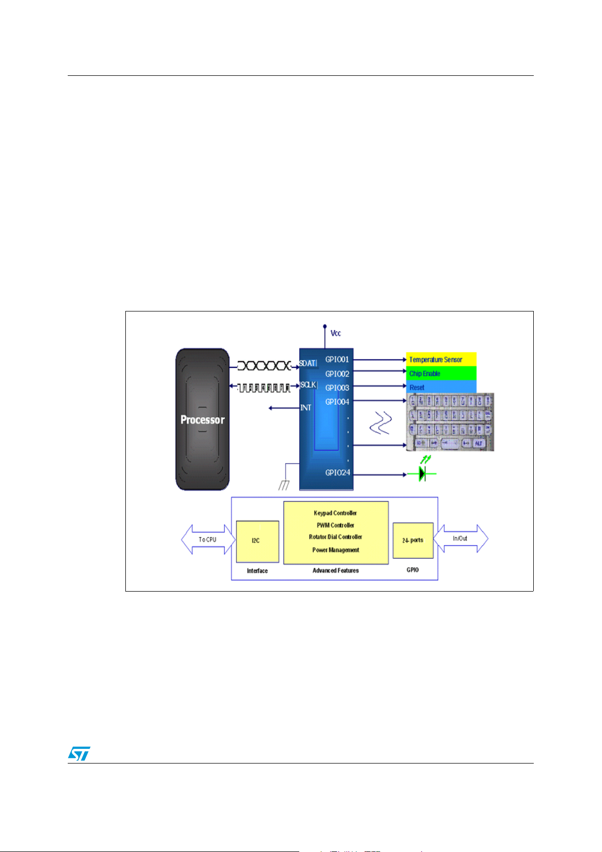
STMPE2401 is the first in the ST family of I/O port expanders. The principle of a basic I/O
port expander is that it provides additional I/Os that can be used by the host processor to
implement additional features such as increased number of inputs/outputs, expanding the
number of control signals and mixed signal lines, controlling a greater number of peripherals
without resorting to an additional Complex Programmable Logic Device (CPLD) or
upgrading the central processing unit (CPU).
In addition to these basic features, the STMPE2401 comes with integrated intelligence to
implement advanced features such as keypad scanning, PWM control, rotator dial control,
etc.
The STMPE2401 can be widely used in the fields of mobile communications, portable
media players, game console, mobile phones, smart phones, consumer electronics and
computer peripherals like state-of-the-art printers, advanced embedded systems, etc.
This application note deals with the setup and hardware interfacing of the device to perform
various functions and the different modes for reducing power consumption.
January 2007 Rev 1 1/19
www.st.com

Contents AN2422
Contents
1 Advantageous features of STMPE2401 . . . . . . . . . . . . . . . . . . . . . . . . . . 3
2 STMPE2401 Hardware description . . . . . . . . . . . . . . . . . . . . . . . . . . . . . 4
2.1 STMPE2401 pin description . . . . . . . . . . . . . . . . . . . . . . . . . . . . . . . . . . . . 6
2.2 Power supply and ground . . . . . . . . . . . . . . . . . . . . . . . . . . . . . . . . . . . . . . 7
2.3 32-kHz crystal oscillator . . . . . . . . . . . . . . . . . . . . . . . . . . . . . . . . . . . . . . . 7
2.4 I2C Interface . . . . . . . . . . . . . . . . . . . . . . . . . . . . . . . . . . . . . . . . . . . . . . . . 8
2.5 Reset pin . . . . . . . . . . . . . . . . . . . . . . . . . . . . . . . . . . . . . . . . . . . . . . . . . . 9
2.6 Interrupt pin . . . . . . . . . . . . . . . . . . . . . . . . . . . . . . . . . . . . . . . . . . . . . . . . 9
2.7 Initialization and configuration of Interrupt Controller . . . . . . . . . . . . . . . . 10
2.8 GPIO state description . . . . . . . . . . . . . . . . . . . . . . . . . . . . . . . . . . . . . . . 10
2.9 Configuring the GPIO Alternate Function register . . . . . . . . . . . . . . . . . . 11
2.10 GPIO Hotkey feature description . . . . . . . . . . . . . . . . . . . . . . . . . . . . . . . 14
2.10.1 GPIO Hotkey programming sequence . . . . . . . . . . . . . . . . . . . . . . . . . . 14
2.10.2 Minimum pulse width . . . . . . . . . . . . . . . . . . . . . . . . . . . . . . . . . . . . . . . 15
2.11 Modes of operation . . . . . . . . . . . . . . . . . . . . . . . . . . . . . . . . . . . . . . . . . . 15
2.11.1 Operational mode . . . . . . . . . . . . . . . . . . . . . . . . . . . . . . . . . . . . . . . . . 15
2.11.2 Sleep mode . . . . . . . . . . . . . . . . . . . . . . . . . . . . . . . . . . . . . . . . . . . . . . 15
2.11.3 Hibernate mode . . . . . . . . . . . . . . . . . . . . . . . . . . . . . . . . . . . . . . . . . . . 15
2.11.4 Typical ICC values in various modes . . . . . . . . . . . . . . . . . . . . . . . . . . . 17
2.12 Power-up sequence . . . . . . . . . . . . . . . . . . . . . . . . . . . . . . . . . . . . . . . . . 17
2.13 Tips for hardware troubleshooting . . . . . . . . . . . . . . . . . . . . . . . . . . . . . . 17
3 Conclusion . . . . . . . . . . . . . . . . . . . . . . . . . . . . . . . . . . . . . . . . . . . . . . . . 18
4 Reference documents . . . . . . . . . . . . . . . . . . . . . . . . . . . . . . . . . . . . . . . 18
5 Revision history . . . . . . . . . . . . . . . . . . . . . . . . . . . . . . . . . . . . . . . . . . . 18
2/19
AN2422 Advantageous features of STMPE2401
1 Advantageous features of STMPE2401
1. A highly flexible interrupt system eliminates the need for polling and reduces CPU
usage
2. Low power consumption
3. Wake-up from Sleep mode
4. Easy-to-use driver software
5. Flexibility in the configuration of individual GPIOs
6. Simpler connection to CPU (just two I
communication
7. Combinational keys to enhance gaming experience
8. Applications: Mobile phone keypads, all-in-one printers, game consoles, embedded
systems, portable media players, etc.
Figure 1. Concept of GPIO port expander
2
C lines + Interrupt pin) for configuration and
3/19

STMPE2401 Hardware description AN2422
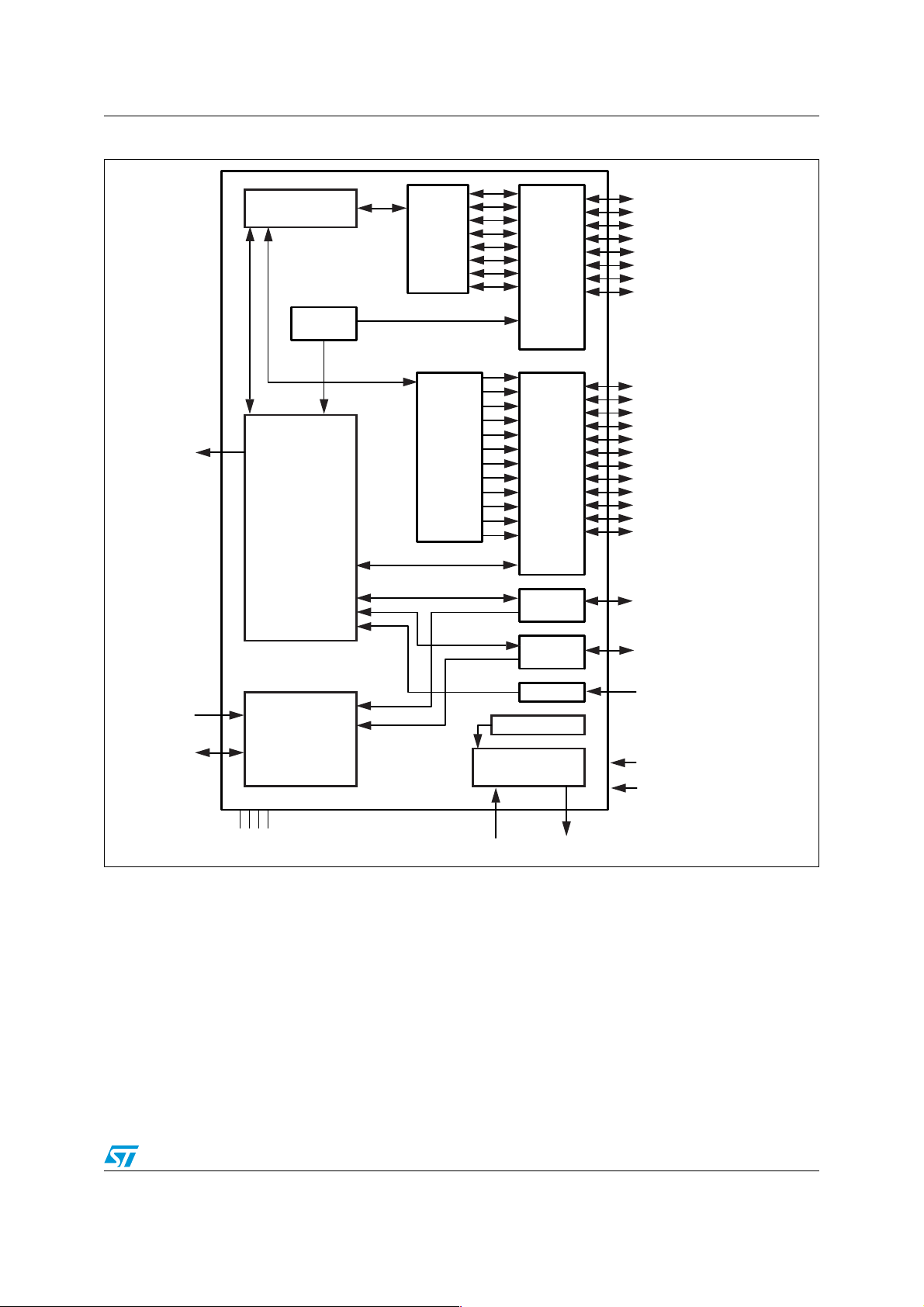
2 STMPE2401 Hardware description
The STMPE2401 is a GPIO (General Purpose Input/Output) port expander able to interface
to a digital application-specific integrated circuit (ASIC) via the two-line bidirectional bus
2
(I
C).
A separate GPIO Expander IC is often used in Mobile-Multimedia platforms to solve the
problems of the limited GPIOs usually available on the Digital Engine.
The STMPE2401 offers great flexibility as each I/O is configurable as input, output or in
specific functions, to scan a keyboard, provide PWM outputs for brightness control in
backlighting or in a rotator decoder interface. This device is designed for use with a very low
quiescent current, and includes a wake-up feature for each I/O to optimize the power
consumption of the IC. The main features of the port expander device are:
● 24 GPIOs
● Operating voltage 1.8V
● Hardware keypad controller (8*12 Matrix maximum)
● 3 PWM (8-bit) outputs for LED brightness control and LED blinking
● Interrupt output (open drain) pin
● Configurable hotkey feature on each GPIO
● Ultra-low Standby-mode Current
● Small Package TFBGA - 36 pins, 3.6x3.6mm and 0.5mm pitch making it optimal for use
in portable applications such as mobile phones with critical space constraints.
4/19
AN2422 STMPE2401 Hardware description
Figure 2. STMPE2401 block diagram
Keypad
Controller
GPIOs
7:0
Keypad
Inputs
Function
Select
Keypad Inputs 7:0
GPIOs 7:0
INT
SCLK
S DATA
Controller Core
+PWM
+Rotator Control
+GPIO Control
2
I²C Interface
GND
A0
A1
Keypad
Outputs
Function
Select
GPIO
15
PWM
O/P
POR
RC Oscillator
Clock
Controller
XTALIN XTALOUT
Keypad Outputs 11:0
GPIOs 14:8 and 20:16
Rotator
GPIO 15
Addr0
PWM1, 2 and 3
Addr1
GPIOs 23:21
Reset_N
CC1
CC2
V
CC1
V
CC2
Ai12531
5/19

STMPE2401 Hardware description AN2422
2.1 STMPE2401 pin description
Ta bl e 1 describes all the pins on the STMPE2401 device.
Table 1. STMPE2401 Pin list
Pin Name Type Description
1GND -
2 KP_X0 IO GPIO
3 Reset_N I External reset input, active LOW
4 KP_X1 IO GPIO
5 KP_X2 IO GPIO
6 KP_X3 IO GPIO
7 KP_X4 IO GPIO
8 KP_X5 IO GPIO
9 KP_X6 IO GPIO
10 GND -
11 V
CC1
12 KP_X7 IO GPIO
13 KP_Y5 IO GPIO
14 KP_Y4 IO GPIO
15 KP_Y3 IO GPIO
16 KP_Y2 IO GPIO
17 KP_Y1 IO GPIO
18 KP_Y0 IO GPIO
19 GND -
20 ADDR0 IO GPIO and I
21 KP_Y9 A/IO GPIO
22 KP_Y10 A/IO GPIO
23 KP_Y11 A/IO GPIO
24 PWM3 A/IO GPIO and I
25 PWM2 A/IO GPIO
26 PWM1 A/IO GPIO
27 V
CC2
28 GND -
29 INT O Open drain interrupt output pin
30 KP_Y8 IO GPIO
31 KP_Y7 IO GPIO
32 KP_Y6 IO GPIO
33 SDATA A I
34 SCLK A I
35 XTALIN A XTAL oscillator or external 32-kHz input
36 XTALOUT A XTAL oscillator
- 1.8V Input
- 1.8V Input
2
C DATA
2
C clock
2
C ADDR 0 (in reset)
2
C ADDR 1 (in reset)
6/19

AN2422 STMPE2401 Hardware description
2.2 Power supply and ground
The STMPE2401 device functions on a 1.8V supply. The core voltage and IO supply voltage
are the same. Proper decoupling capacitors should be used to filter out the power supply
noise.
● Both V
CC1
and V
pins can be shorted together and supplied with the same 1.8V
CC2
supply.
● All four GND pins should be connected together and grounded.
2.3 32-kHz crystal oscillator
The 32-kHz clock can be supplied either externally or through a 32-kHz crystal oscillator.
When using an external clock, the signal should be pumped in directly at the XTALIN pin
and XTALOUT pin should be left open. The frequency of the clock can be less than 32 kHz
but should not exceed 32 kHz. The clock amplitude should not exceed 1.8V peak-peak.
An external oscillator of low accuracy (between 16 and 32 kHz) can also be used as a
source for the 32-kHz clock input. This helps reduce cost by permitting the use of an
inexpensive oscillator instead of an expensive, very high accuracy on-board oscillator.
If using a 32-kHz crystal oscillator, the crystal should be connected across the XTALIN and
XTALOUT pins. The filter capacitors of 27pF should be added externally at each pin as near
the crystal pins as possible.
Figure 3. 32-kHz crystal oscillator connection
1
2
Y1
32-kHz
1
Crystal Oscillator
Ai12532
STMPE2401
XTALOUT
XTALIN
SCLK
SDATA
36
35
SCLK
SDATA
C2
27pF
C3
27pF
The device has an internal RC oscillator to generate a 5-MHz clock typically using the 32kHz input. During Sleep and Hibernate modes, this oscillator is switched off to reduce power
consumption.
7/19

STMPE2401 Hardware description AN2422
2.4 I2C Interface
The STMPE2401 port expander can be controlled using just the two I2C lines. All internal
registers can be accessed through this I
2
C interface. The I
2
C interface features are as given
below:
2
● I
C Slave device
● Operates at 1.8V
● Compliant with Philip I
● Supports Standard (up to 100 kbps) and Fast (up to 400 kbps) modes
● 7-bit addressing mode supported
● Start/Restart/Stop
● Up to 4 STMPE2401 devices can be connected on the same I
2
C specification version 2.1
2
C bus
The slave address is selected by the state of two pins (GPIO15 and GPIO23). The state of
the pins is latched into STMPE2401 at power-on and these address settings are retained
until the power is switched off. The
added as the LSB to the 7-bit slave address to make up one byte to be sent through the
I2C Read/Write is performed byte by byte. The R/W bit is
I2C
interface from the Master.
Table 2. Valid I
ADDR1
(GPIO23)
0 0 42h (100 0010b) 84h
0 1 43h (100 0011b) 86h
1 0 44h (100 0100b) 88h
2
C slave address
ADDR0
(GPIO15)
7-bit Slave
Address
8-bit format to be
used (including R/W
bit in LSB)
1 1 45h (100 0101b) 8Ah
Once the slave address is configured and responding correctly, the internal registers can be
accessed through I
The SCLK and SDATA are open drain pins and should be provided with pull-up resistors for
proper functioning. These two pins are 3.6V tolerant and hence can be driven directly by I
master devices operating within the range of 1.8V to 3.6V. The pull-up resistors should be
connected to the corresponding I
Figure 4. I
2
C interface.
2
C host VCC as indicated in Figure 4.
2
C lines with external pull-up resistors
3.3V
4.7kΩ
4.7kΩ
Host
3.3V
1.8V
STMPE2401
SCLK
SDATA
Ai12530a
2
C
8/19
AN2422 STMPE2401 Hardware description
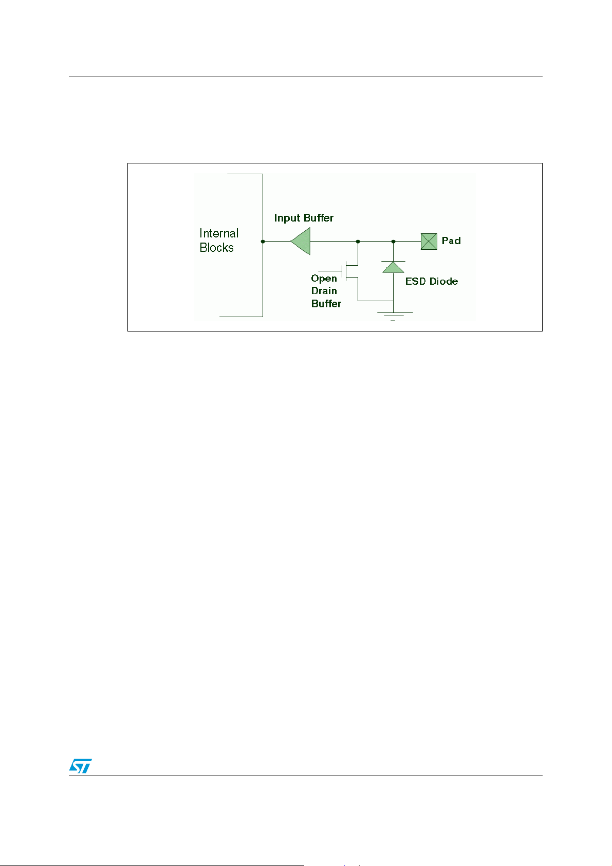
I2C pin structure
Figure 5 shows the SCLK and SDATA pin structures. These structures enable the driving
signal voltages to be higher than the VCC without causing any damage.
Figure 5. SCLK and SDATA pin structure
2.5 Reset pin
The RESET_N pin is an active low input. It should be tied HIGH in order to start normal
operation of the device. Other than the RESET_N pin, the device can also be reset through
the “Soft_Reset” bit in the SYSCON register. Writing a '1' to this bit resets the device and
after reset, the bit is cleared to '0' by hardware.
Note: The device reset phase lasts for 200µs during which no I
2.6 Interrupt pin
The Interrupt (INT) pin is an open-drain output pin and should have an external pull-up
resistor to VCC. The interrupt output can be configured as a level or edge-triggered interrupt
by setting Bit 1 in the ICR register. The polarity can be set by Bit 2 in the ICR register. The
interrupt pin will remain low regardless of the Interrupt settings until the Global Interrupt
Mask bit (Bit 0 in ICR register) is set to '1'. At reset, the default interrupt type is Level
Interrupt with Active Low polarity. The INT pin structure is similar to the open drain structure
of the SCLK and SDATA pins.
2
C command is acknowledged.
9/19

STMPE2401 Hardware description AN2422
2.7 Initialization and configuration of Interrupt Controller
● Set the IER and IEGPIOR registers to the desired values to enable the interrupts from
the required sources.
● Configure the output interrupt type (Bit IC1) and polarity (Bit IC2) and enable the global
interrupt mask bit by writing '1' to the IC0 bit of the ICR register.
● Wait for the interrupt.
● When an interrupt is received, the INT pin is asserted as per the selected interrupt type
and polarity.
● The host can read the interrupt status from the ISR register through the I
'1' in the ISR bits indicates that the corresponding interrupt source is triggered. The
host can then perform the necessary operation related to the Interrupt.
● For example, if the IS8 bit in the ISR register is set, the interrupt comes from the GPIO
Controller. Then, a subsequent read can be performed on the ISGPIOR register to
locate the exact GPIO that triggered the interrupt. This is the 'Hotkey Feature' that can
be used to wake-up or trigger an interrupt for the host.
● To clear the interrupt, write '1' via the I
2
C interface to the corresponding IS[x] bit of the
ISR register.
● If the interrupt source is from the GPIO Controller, one additional write operation is
needed to clear the ISG[x] bit in the ISGPIOR register to enable subsequent events to
trigger an interrupt.
● Once the interrupt status is cleared, the INT pin will also be de-asserted if the interrupt
type is level interrupt. An edge interrupt will assert a pulse of only 250 ns.
● To disable sending interrupts to host, reset to ‘0’ the IC0 bit (Global interrupt mask bit)
in the ICR register. Even if the global interrupt is disabled, the interrupt status continues
to be registered in the ISR register.
2
C interface. A
2.8 GPIO state description
All 24 GPIO lines are inputs at power-on/reset. GPIO15 and GPIO23 pins can be used for
other functions once the slave address is latched into the device. External pull-up or pulldown resistors on these pins can be used to set the I
All 24 GPIOs are independent of each other and can be individually programmed as inputs
or outputs. The GPIOs can also be configured to serve as alternate functions: keypad
module, PWM module and rotator modules (based on the GPIO Alternate function register
(GPAFR) settings). Figure 6 gives the pin structure of the GPIO pins.
10/19
2
C address at power-up.

AN2422 STMPE2401 Hardware description
Figure 6. GPIO pin structure
2.9 Configuring the GPIO Alternate Function register
Ta bl e 7 lists the alternate functions of each GPIO. When configuring the STMPE2401 for
built-in functions such as Keypad Control, PWM control or Rotator function, only the
corresponding GPIOs should be used.
Ta bl e 3 lists an example alternate function configuration involving all 24 GPIOs.
Table 3. GPIO Alternate function configuration example
GPIO Description
7:0 Alternate Function 1 (Keypad inputs 0 to 7)
16, 14:8 Alternate Function 1 (Keypad outputs 0 to 7)
15 Hotkey Input with internal pull-up resistor (Primary GPIO function)
17 Alternate Function 3 (CLKOUT for cascading two STMPE2401 devices)
20:18 Alternate Function 2 (Rotator)
23:21 Alternate Function 1 (PWM channels)
To select the function for each GPIO pin, the corresponding bit-pair in the GPAFR registers
(GPAFR_U (Ta b le 4 ) or GPAFR_L (Ta b le 5 )) must be set as described in Tab le 6 .
Table 4. GPAFR_U register
GPAFR_U_msb
Bit 2322212019181716
GPIO23 AF GPIO22 AF GPIO21 AF GPIO20 AF
Example setting01010110
11/19

STMPE2401 Hardware description AN2422
Table 4. GPAFR_U register (continued)
GPAFR_U_csb
Bit 151413121110 9 8
GPIO19 AF GPIO18 AF GPIO17 AF GPIO16 AF
Example setting10101101
GPAFR_U_lsb
Bit 76543210
GPIO15 AF GPIO14 AF GPIO13 AF GPIO12 AF
Example setting00010101
Table 5. GPAFR_L register
GPAFR_L_msb
Bit 2322212019181716
GPIO11 AF GPIO10 AF GPIO9 AF GPIO8 AF
Example setting 01010101
GPAFR_L_csb
Bit 151413121110 9 8
GPIO7 AF GPIO6 AF GPIO5 AF GPIO4 AF
Example setting 01010101
GPAFR_L_lsb
Bit 76543210
GPIO3 AF GPIO2 AF GPIO1 AF GPIO0 AF
Example setting 01010101
Table 6. GPAFR register bit description
GPIO[x] AF Description
‘00’
‘01’
‘10’
‘11’
The corresponding GPIO pin (GPIO[x]) is configured to Primary Function
The corresponding GPIO pin (GPIO[x]) is configured to Alternate Function 1
The corresponding GPIO pin (GPIO[x]) is configured to Alternate Function 2
The corresponding GPIO pin (GPIO[x]) is configured to Alternate Function 3
12/19

AN2422 STMPE2401 Hardware description
Ta bl e 7 lists the alternate functions by pin name.
Table 7. GPIO alternate functions
Pin Name Primary Function
Alternate
Function 1
Alternate
Function 2
KP_X0 GPIO 0 Keypad input 0
KP_X1 GPIO 1 Keypad input 1
KP_X2 GPIO 2 Keypad input 2
KP_X3 GPIO 3 Keypad input 3
KP_X4 GPIO 4 Keypad input 4
KP_X5 GPIO 5 Keypad input 5
KP_X6 GPIO 6 Keypad input 6
KP_X7 GPIO 7 Keypad input 7
KP_Y5 GPIO 13 Keypad output 5
KP_Y4 GPIO 12 Keypad output 4
KP_Y3 GPIO 11 Keypad output 3
KP_Y2 GPIO 10 Keypad output 2
KP_Y1 GPIO 9 Keypad output 1
KP_Y0 GPIO 8 Keypad output 0
ADDR0 GPIO 15
KP_Y9 GPIO 18 Keypad output 9 Rotator 0
KP_Y10 GPIO 19 Keypad output 10 Rotator 1
Alternate
Function 3
KP_Y11 GPIO 20 Keypad output 11 Rotator 2
PWM3 GPIO 23 PWM CH-3
PWM2 GPIO 22 PWM CH-2
PWM1 GPIO 21 PWM CH-1
KP_Y8 GPIO 17 Keypad output 8 ClkOut
KP_Y7 GPIO 16 Keypad output 7
KP_Y6 GPIO 14 Keypad output 6
Each GPIO can be individually programmed to generate an interrupt on change of state,
with either falling-edge or rising-edge detection. Every GPIO has a provisional pull-up and
pull-down resistor that can be turned on by configuring the corresponding bit in the GPPUR
(msb, csb or lsb) and GPPDR (msb, csb, lsb) registers.
13/19

STMPE2401 Hardware description AN2422
2.10 GPIO Hotkey feature description
A GPIO is known as 'Hotkey' when it is configured to trigger an interrupt to the host
whenever the GPIO input is asserted. This can also be used to Wake-up the device from
Sleep Mode. This feature can be enabled both in Operational mode (RC clock is present) as
well as in Sleep mode (only 32-kHz clock is present). The hotkey assertion can be detected
either as a falling edge event (GPIO is normally pulled high) or as a rising edge event (GPIO
is normally pulled low) in the GPEDR register. The pull-up/pull-down condition can be
implemented using either external resistors as shown in Figure 7 or configured with internal
resistors through the GPPUR and GPPDR registers.
Figure 7. Hotkey detection using external pull-up/pull-down resistors on GPIO
10k
10k
Ω
Ω
STMPE2401
Host
GPIO
Controller
2.10.1 GPIO Hotkey programming sequence
1. The required GPIO pin should be configured as an input using the GPDR register.
2. The GPIO should be set in the default GPIO function mode with the corresponding bits
in GPAFR register set to '00'.
3. If internal resistors are required, enable the corresponding resistor in the GPPUR and
GPPDR registers.
4. Set the GPRER and GPFER registers to the desired values to enable the rising edge or
falling edge detection on the respective GPIO.
5. Configure and enable the interrupt controller to allow the interrupt to the host through
the ICR register. The type and polarity of the interrupt to be generated should also be
set through the same register.
6. To generate an edge triggered GPIO interrupt, the corresponding bit should be enabled
in the IEGPIOR register. If this is not enabled, the event is registered in the GPEDR,
ISGPIOR and ISR registers but no wake-up interrupt is triggered and consequently the
device does not come out of Sleep mode.
7. Now, the GPIO Expander may be put into Sleep mode if it is desired.
8. When any Hotkey is asserted, the device wakes up and issues an interrupt to the host.
Hotkey Signal 1
SW1
Hotkey Signal 2
SW2
Ai12533
14/19

AN2422 STMPE2401 Hardware description
2.10.2 Minimum pulse width
The minimum pulse width of the signal asserting the Hotkey must be at least 62.5 µs. Any
signal with a pulse width less than the stated value may not be registered.
2.11 Modes of operation
2.11.1 Operational mode
This is normal operation mode of the device. In this mode, the RC clock is available and the
Controller core routes this clock and the 32-kHz clock to all the device blocks that are
enabled. The individual blocks that are not used can be turned off by the Master by
programming Bits 3 to 0 of the SYSCON register.
2.11.2 Sleep mode
In this low-power mode, the internal RC Oscillator is powered down. All the blocks which
need clocks derived from the 32-kHz clock will continue getting a 32-kHz clock. In this mode
also, individual blocks can be turned off by the master by programming Bits 3 to 0 of the
SYSCON register. The operating clock is cut off from every functional block (including the
2
I
C interface) except the Keypad Controller and the GPIOs. Therefore, the master needs to
program the SYSCON register before entering this mode; as in Sleep mode, the I
interface is not active except to detect traffic for wakeup.
Any activity on the I
this mode and resume normal operation. When leaving Sleep mode, the I
2
C port or Wakeup pin or Hotkey activity will cause the device to leave
2
C needs to hold
the SCLK until the RC clock stabilizes. This is typically less than 300 µs, however it is
recommended to wait for the Wake-up Interrupt to be asserted before resuming I
command operations. The device enters Sleep mode by writing '1' to Bit 4 in SYSCON
register.
2
C
2
C
2.11.3 Hibernate mode
This mode is entered when the system writes a '1' to bit 5 of the SYSCON register. In this
mode, the device is completely inactive and no clock is present. Only a Reset or a wakeup
2
on I
C will bring back the System into Operational mode. Hotkey wakeup is also not possible
in Hibernate mode.
Table 8. I
Start
1. Shaded=Slave,
otherwise, Master.
There is a 300-µs latency between the I2C wake-up command and device wake-up. During
this interval, the STMPE2401 does not acknowledge the device address (whether in
Sleep/Hibernate mode).
2
C wake-up packet format
NACK
RnW=0
Dev Addr
(1)
Stop
15/19

STMPE2401 Hardware description AN2422
Figure 8. Operational modes based on 32-kHz clock domain
Sleep Mode
32K: On
RC: Off
Table 9. One-Byte Read
Start
Dev Addr
1. Shaded=Slave, otherwise, Master.
Table 10. Multiple-Byte Read
Start
Dev Addr
1. Shaded=Slave, otherwise, Master.
Table 11. One-Byte Write
RnW=0
RnW=0
ACK
Reg Addr
ACK
Reg Addr
(1)
ACK
ACK
(1)
Operational Mode
32K: On
RC: On
Any
Wakeup
Wakeup_i2c
reSTart
Dev Addr
(1)
reSTart
Dev Addr
RnW=1
RnW=1
ACK
ACK
Data Read
Data Read
NACK
ACK
Clock_off_32K
Hibernate Mode
32K: Off
RC: Off
Stop
... ...
ACK
Data Read + 1
Reset
Data Read + n
Stop
NACK
Start
Dev Addr
1. Shaded=Slave, otherwise, Master.
Table 12. Multiple-Byte Write
Start
Dev Addr
1. Shaded=Slave, otherwise, Master.
ACK
RnW=0
ACK
RnW=0
Reg Addr
Reg Addr
ACK
Data to be
ACK
(1)
written
ACK
ACK
Data Write
16/19
Stop
Data Write + 1
... ...
ACK
ACK
Stop
Data Write + n

AN2422 STMPE2401 Hardware description
2.11.4 Typical ICC values in various modes
Table 13. Typical operating current measurements
Operating modes Typical ICC consumption at TA = 25°C
Normal operation mode 450~650 µA
Sleep mode 5.5~7.0 µA
Hibernate mode 3.5~4.5 µA
2.12 Power-up sequence
1. All four GND pins of device should be shorted and grounded.
2. If a 32-kHz crystal oscillator is not used, an external 32-kHz clock and 1.8Vpk-pk
voltage should be supplied on the XTALIN pin.
3. The
4. The RESET_N pin should be connected to V
5. The ADDR0 and PWM3 pins should be hard-coded with the correct slave address.
I2C lines, SCLK and SDATA, should be connected to the host. Both lines should
have pull-up resistors to 1.8V.
.
CC
These lines can be released for other functions once the slave address is latched at
Reset. These pins can be hard-coded using external weak pull-up and pull-down
resistors.
Note: The state of the address pins should be stable before the device is powered.
6. Both V
CC1
and V
should be shorted and connected to 1.8V supply with proper
CC2
decoupling capacitors.
7. The INT pin should also be connected to VCC via an external pull-up resistor.
With these minimal connections, the device should start functioning in normal mode
providing I
2
C access to the internal registers. All GPIOs are in default input mode and the
INT output state is LOW regardless of the interrupt register settings until the Global Interrupt
mask bit is enabled in the SYSCON register.
2.13 Tips for hardware troubleshooting
If the device does not function at the end of the power-up sequence described above, the
following tips can be used for troubleshooting.
1. All pins are provided with an internal reverse-biased ESD protection diode to GND.
Verify the connectivity of the pins in relation to GND.
2. The normal I
is between 450 and 650 µA. Verify this value at power-on.
3. When the clock frequency is reduced from 32 kHz, the I
not, verify the device connections again.
current drawn by the device with the minimal connections at power-up
CC
should also drop slightly. If
CC
17/19

Conclusion AN2422
3 Conclusion
The STMPE2401 is a very versatile device that can be used to reduce the load on the CPU
and expand the number of IOs available for the processor. Its small size and built-in
intelligence modules make it a very attractive proposition for high-end, portable applications
such as smart phones.
This application note provides the setup information to interface this device with any digital
engine. The configuration and functioning of the internal keypad controller and PWM
module are provided in other separate application notes.
4 Reference documents
Application note AN2423: STMPE2401 - Port Expander keypad controller
Application note AN2424: STMPE2401 - Port Expander PWM controller
5 Revision history
Table 14. Document revision history
Date Revision Changes
18-Jan-2007 1 Initial release.
18/19

AN2422
Please Read Carefully:
Information in this document is provided solely in connection with ST products. STMicroelectronics NV and its subsidiaries (“ST”) reserve the
right to make changes, corrections, modifications or improvements, to this document, and the products and services described herein at any
time, without notice.
All ST products are sold pursuant to ST’s terms and conditions of sale.
Purchasers are solely responsible for the choice, selection and use of the ST products and services described herein, and ST assumes no
liability whatsoever relating to the choice, selection or use of the ST products and services described herein.
No license, express or implied, by estoppel or otherwise, to any intellectual property rights is granted under this document. If any part of this
document refers to any third party products or services it shall not be deemed a license grant by ST for the use of such third party products
or services, or any intellectual property contained therein or considered as a warranty covering the use in any manner whatsoever of such
third party products or services or any intellectual property contained therein.
UNLESS OTHERWISE SET FORTH IN ST’S TERMS AND CONDITIONS OF SALE ST DISCLAIMS ANY EXPRESS OR IMPLIED
WARRANTY WITH RESPECT TO THE USE AND/OR SALE OF ST PRODUCTS INCLUDING WITHOUT LIMITATION IMPLIED
WARRANTIES OF MERCHANTABILITY, FITNESS FOR A PARTICULAR PURPOSE (AND THEIR EQUIVALENTS UNDER THE LAWS
OF ANY JURISDICTION), OR INFRINGEMENT OF ANY PATENT, COPYRIGHT OR OTHER INTELLECTUAL PROPERTY RIGHT.
UNLESS EXPRESSLY APPROVED IN WRITING BY AN AUTHORIZED ST REPRESENTATIVE, ST PRODUCTS ARE NOT
RECOMMENDED, AUTHORIZED OR WARRANTED FOR USE IN MILITARY, AIR CRAFT, SPACE, LIFE SAVING, OR LIFE SUSTAINING
APPLICATIONS, NOR IN PRODUCTS OR SYSTEMS WHERE FAILURE OR MALFUNCTION MAY RESULT IN PERSONAL INJURY,
DEATH, OR SEVERE PROPERTY OR ENVIRONMENTAL DAMAGE. ST PRODUCTS WHICH ARE NOT SPECIFIED AS "AUTOMOTIVE
GRADE" MAY ONLY BE USED IN AUTOMOTIVE APPLICATIONS AT USER’S OWN RISK.
Resale of ST products with provisions different from the statements and/or technical features set forth in this document shall immediately void
any warranty granted by ST for the ST product or service described herein and shall not create or extend in any manner whatsoever, any
liability of ST.
ST and the ST logo are trademarks or registered trademarks of ST in various countries.
Information in this document supersedes and replaces all information previously supplied.
The ST logo is a registered trademark of STMicroelectronics. All other names are the property of their respective owners.
© 2007 STMicroelectronics - All rights reserved
STMicroelectronics group of companies
Australia - Belgium - Brazil - Canada - China - Czech Republic - Finland - France - Germany - Hong Kong - India - Israel - Italy - Japan -
Malaysia - Malta - Morocco - Singapore - Spain - Sweden - Switzerland - United Kingdom - United States of America
www.st.com
19/19
 Loading...