

Page 1

AN2389
Application note
An MCU-based low cost non-inverting
buck-boost converter for battery chargers
Introduction
As the demand for rechargeable batteries increases, so does the demand for battery
chargers. There are different kinds of design solutions available for implementing battery
chargers. Some of them are dedicated hardware based solutions and some are
microcontroller based solutions.
In a microcontroller based solution, you have the flexibility of using the same hardware for
charging different batteries and making only slight changes in the software. But there are
still some challenges and one of the major challenges is to have a suitable input power
supply available. Generally the Buck converter topology is used as a DC- DC converter to
provide the controlled output power supply to the batteries. But in this case a problem may
arise, for example, if you want to charge a 4.2V Li-ion batteries from a 5V supply due to the
presence of the protection diode and other small drops across other components. This drop
is generally about 1V which makes it very difficult to provide 4.2V to the Li-ion batteries
using the buck converter topology.
This application note describes a simple technique for implementing a non-inverting buckboost converter which requires only one inductor. This converter is basically the result of
cascading a Buck converter with a Boost converter. This converter can be controlled by two
PWM signals from the microcontroller and can be used as a Buck converter or Boost
converter whenever required. So this solution combined with the flexibility of the ST7
microcontroller can be used to charge a wide range of the batteries using the same
hardware.
The example used in this application note is specific to battery chargers but this DC-DC
converter can be very useful for portable applications in general or any application which
uses rechargeable batteries.
August 2007 Rev 1 1/16
www.st.com
Page 2

Contents AN2389
Contents
1 Circuit diagram . . . . . . . . . . . . . . . . . . . . . . . . . . . . . . . . . . . . . . . . . . . . . 3
2 Theory of operation . . . . . . . . . . . . . . . . . . . . . . . . . . . . . . . . . . . . . . . . . 4
2.1 Buck-boost implementation . . . . . . . . . . . . . . . . . . . . . . . . . . . . . . . . . . . . 4
2.2 Buck converter implementation . . . . . . . . . . . . . . . . . . . . . . . . . . . . . . . . . 6
2.3 Boost converter implementation . . . . . . . . . . . . . . . . . . . . . . . . . . . . . . . . . 7
3 Selection of components . . . . . . . . . . . . . . . . . . . . . . . . . . . . . . . . . . . . . 8
3.1 Inductor selection . . . . . . . . . . . . . . . . . . . . . . . . . . . . . . . . . . . . . . . . . . . . 8
3.2 Capacitor selection . . . . . . . . . . . . . . . . . . . . . . . . . . . . . . . . . . . . . . . . . . . 8
4 Application in battery charger . . . . . . . . . . . . . . . . . . . . . . . . . . . . . . . . . 9
4.1 Theory of operation . . . . . . . . . . . . . . . . . . . . . . . . . . . . . . . . . . . . . . . . . . 9
4.2 Software flowchart . . . . . . . . . . . . . . . . . . . . . . . . . . . . . . . . . . . . . . . . . . 10
5 Test environment and results . . . . . . . . . . . . . . . . . . . . . . . . . . . . . . . . . 11
6 Conclusion . . . . . . . . . . . . . . . . . . . . . . . . . . . . . . . . . . . . . . . . . . . . . . . . 13
7 References . . . . . . . . . . . . . . . . . . . . . . . . . . . . . . . . . . . . . . . . . . . . . . . . 14
8 Revision history . . . . . . . . . . . . . . . . . . . . . . . . . . . . . . . . . . . . . . . . . . . 15
2/16
Page 3
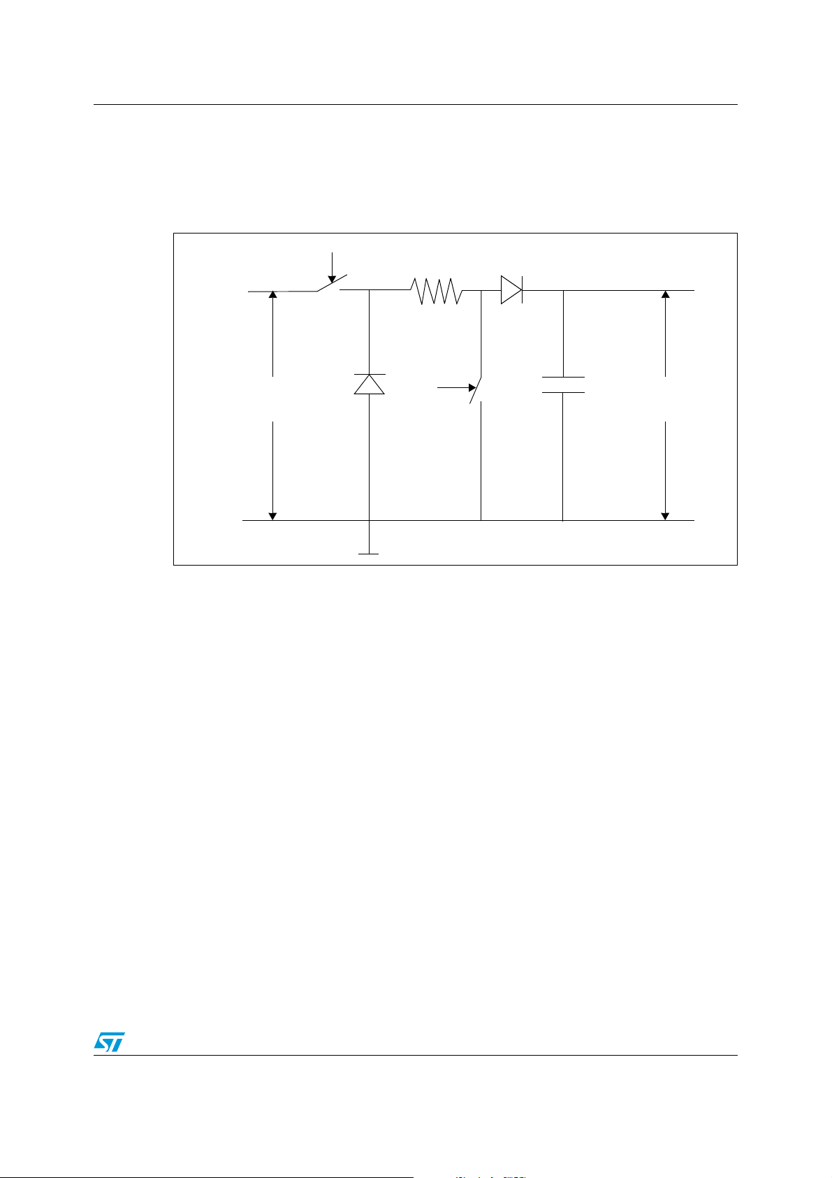
AN2389 Circuit diagram
1 Circuit diagram
The diagram in Figure 1 shows the structure of the modified buck-boost converter.
Figure 1. Modified buck-boost converter
P+
P-
PWM1
SW1
d1
V
IN
L
PWM2
d2
SW2
C
V
OUT
3/16
Page 4

Theory of operation AN2389
2 Theory of operation
You can use this converter as buck-boost converter, as a buck converter or as a boost
converter by selecting different combinations of switches SW1 and SW2 driven by the
PWM1 and PWM2 signals output by the ST7 microcontroller.
2.1 Buck-boost implementation
This converter can be used as a non inverting buck-boost converter by selecting the
operating mode from Tabl e 1 which briefly describes the converter modes.
.
Table 1. Operating modes based on switch combinations
Phase SW1 (PWM1) SW2 (PWM2) Operating modes
1OFF OFF BUCK
2OFF ON N/A
3ON OFF BUCK-BOOST
4ON ON BOOST
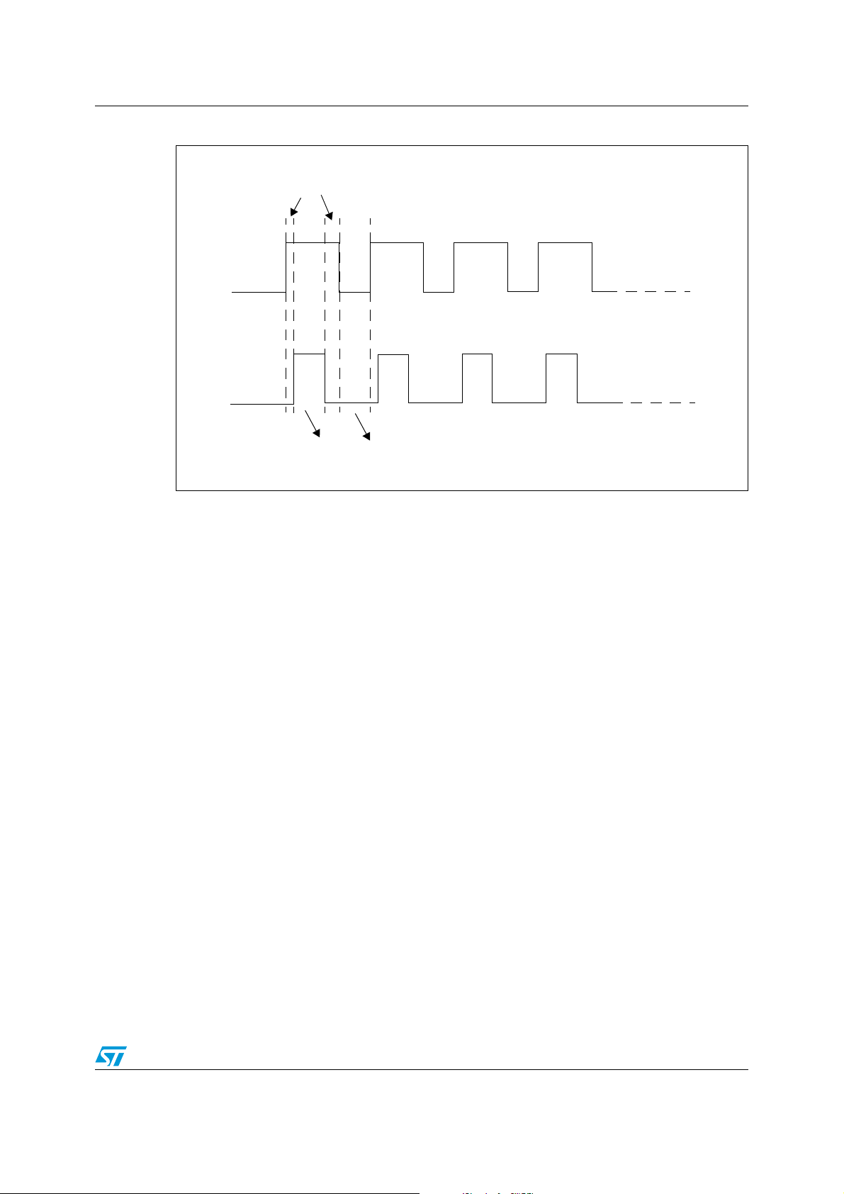
If we look at phase 2 in Ta bl e 1 , here the switch SW1(PWM1) is OFF and switch SW2
(PWM2) is ON. This condition never occurs either in a buck converter or in boost converter.
So you should always take care in your software that this condition must not happen. To
avoid this, if we assume that initially both switches are in OFF condition then you should use
the following guidelines to manage the PWM signals driving the two switches.
1. Keep the frequency of both PWM signals the same, to better control when
synchronizing the two PWM signals using the next three guidelines.
2. The duty cycle D1 of control signal PWM1, must be greater than the duty cycle D2 of
control signal PWM2.
3. PWM1 should be enabled before the PWM2 signal.
4. PWM1 should be disabled after the PWM2 signal.
4/16
Page 5
AN2389 Theory of operation
Figure 2. Timing diagram for two PWM signals
Phase 3
PWM1
PWM2
Phase 1Phase 4
Figure 2 shows a timing example for the two PWM signals based on the above guidelines.
Here phase 2 does not occur.
– If the duty cycles of the two PWM signals driving SW1(PWM1) and SW2 (PWM2)
are D1 and D2 respectively and
– if we exclude the saturation voltage of the switches from our calculation and
– if the drop across the diodes is V
and Vd2 respectively,
d1
– then the output voltage Vout is given by the following formula:
= [ Vin * D1 - V
V
out
* ( 1 - D1) ] / ( 1 - D2) - V
d1
d2
As mentioned in [2], theoretically this converter works linearly over a gain range of 0 - 200%
of the input voltage.
5/16
Page 6

Theory of operation AN2389
2.2 Buck converter implementation
If you keep SW2 always in OFF condition and drive SW1 (PWM1) with a PWM signal from
the microcontroller then the circuit works like a buck converter, except that you have an
additional diode drop V
Figure 3. Buck converter implementation
due to diode d2.
d2
P+
P-
PWM1
d1
V
IN
L
OFF
d2
SW2
C
V
OUT
If the duty cycle of the PWM signal driving SW1 (PWM1) is D1, the output voltage will be
given by:
V
= Vin * D1 - Vd1 ( 1 - D1) - V
out
d2
6/16
Page 7

AN2389 Theory of operation
2.3 Boost converter implementation
Again if you keep switch SW1 (PWM1) always in ON condition and drive the Switch SW2
(PWM2) with a PWM signal generated by the microcontroller, then the combination works as
a boost converter except that you have an additional free wheeling diode D1 which you can
ignore.
Figure 4. Boost converter implementation
P+
V
IN
P-
If the input voltage is V
across the diode d2 is V
= Vin / ( 1 - D2) - V
V
out
ON
SW1
d1
, the duty cycle of the PWM signal driving PWM2 is D2 and the drop
in
, then the output voltage V
d2
d2
L
PWM2
d2
SW2
is given by:
out
C
V
OUT
7/16
Page 8

Selection of components AN2389
3 Selection of components
The inductor and capacitor can be selected using the formulae given below.
3.1 Inductor selection
The minimum value of the inductor can be selected by choosing the maximum of the values
given by the following two formulae:
T * [ ( Vin - V
2 * I
Lmin =
are the saturation voltages of the two switches SW1 and SW2.
Here V
sat1
and V
Lmin =
sat2
Iout and Vout are the maximum output current and voltage respectively.
V
and Vd2 is the drop across diodes d1 and d2.
d1
The duty cycles of the PWM signals driving SW1 and SW2 are D1 and D2 respectively.
3.2 Capacitor selection
The minimum of the capacitor value can be selected by using the following formula ,
assuming a variation in Vout of 1% or less
In practice, we take inductor and capacitor values that are larger than the values calculated
using the above formulae.
out
T * [ Vd1 + V
2 * I
Cmin =
) * D1 - V
sat1
out
100 * I
V
out
out
out
* D2 - V
sat2
] * ( 1 - D1)
* (1 - D1) * T
* (D1 - D2)]
out
(1)
(2)
(3)
8/16
Page 9

AN2389 Application in battery charger
4 Application in battery charger
We can use the modified non-inverting buck-boost converter in a combination of different
modes as required by the application.
4.1 Theory of operation
The DC-DC converter uses a combination of buck-boost converter and boost converter
mode to charge the Li-ion battery. In case of Li-ion, the constant current constant voltage
(CC CV) charging algorithm is used to charge the battery. Here we have chosen the input
voltage just enough to show the functionality of the converter in buck-boost mode and boost
mode.
Initially the converter works in Buck-Boost converter mode to charge the battery in constant
current mode by keeping the duty cycle of PWM2 constant and varying the duty cycle of
PWM1. As soon as there is an overflow condition for the duty cycle of PWM1. The converter
switches from buck-boost converter mode to boost converter mode. And then duty cycle of
PWM2 is varied to follow the algorithm while SW1 remains in ON condition. Following
section shows the software flow chart for this combination.
9/16
Page 10

Application in battery charger AN2389
4.2 Software flowchart
There are many ways in which you can control the operation of this circuit. An example
algorithm which can be used for in Li-ion battery charger is given below-
Figure 5. Li-ion battery charger flowchart
INITIALIZE THE PWM
SIGNALS WITH DUTY
CYCLE D1 AND D2.
WORKS IN BUCK-BOOST MODE. KEEP D2
FIXED AND VARY D1 TO KEEP THE CURRENT
CONSTANT.
IS THERE
A OVERFLOW IN
D1?
YES
WORKS IN BOOST MODE. KEEP SW1
ALWAYS ON AND VARY THE D2 TO
CONTINUE THE ALGORITHM BY KEEP
-ING THE CURRENT OR VOLTAGE
CONSTANT AS REQUIRED.
END
No
10/16
Page 11

AN2389 Test environment and results
5 Test environment and results
We used this buck-boost converter in the universal battery charger evaluation board
described in AN2390. Figure 6 below shows the general battery charger circuit using the
non-inverting buck-boost converter circuit mentioned in this application note. For simplicity,
this figure does not show all the connections.
Figure 6. General circuit-based battery charger
P+
P-
PWM1
SW1
d1
V
IN
L
PWM2
d2
SW2
I
BAT
C
V
OUT
V
BAT
Battery
R
S
Sense resistor
Here some results are shown for charging the Li-ion battery using this converter in buckboost mode. The above charger is is intended for charging a single Li-ion or two NiMH in
series using a 5V supply input. Details on the implementation are given in AN2390 where
you can find results for NiMH batteries as well as for a charger used simply in buck
converter mode.
Some parameter values are as follows:
V
= 5V, Iin (MAX) = 2A, V
in
sat1
= V
= 0.3V, Vd1 = V
sat2
= 0.5V. and PWM frequency for both
d2
PWM1 and PWM2 = 16KHz.
Also let’s say the maximum value of V
= 5.5V and I
out
= 1.2A and the maximum duty cycle
out
of D1 is 95% and D2 is equal to 30%.
Then using the formulas given in Section 3:
Lmin = 21 uH (from equation 1) or 10 uH (from equation 2). So we should choose a value
larger than 21 uH.
Cmin = 70uF (from equation 3). So we need to choose a value higher than 70 uF.
In this example, L = 75 uH, C = 470 uF are taken, which are larger than the values
calculated using the formulas hence will support the application.
The following table shows some of the readings taken for different values of the duty cycles
D1 and D2.
11/16
Page 12

Test environment and results AN2389
I
Table 2. Input vs output
Sl No Vin (V) Iin (A) V
(V) I
out
out
(A)
1 5 1.23 3.9 1.05
2 5 1.33 4.14 1.05
3 5 1.36 4.2 1.05
4 5 1.27 4.2 0.975
5 5 0.97 4.2 0.80
6 5 0.85 4.2 0.712
7 5 0.65 4.15 0.55
8 5 0.33 4.15 0.28
9 5 0.31 4.15 0.26
10 5 0.16 4.10 0.129
In above results, we have not added V
(0.3V), diode drop (0.5V) and the drop across the
sat
series resistor (connected to measure battery current) as shown in Figure 6 to get the actual
output voltage of the non-inverting buck-boost converter.
For example it is given that V
(battery voltage) = 4.2V,
out
but the actual output voltage of the converter is equal to:
V
4.2V (Battery Voltage V
out
) + 0.3V(Switch Drop V
bat
)+ 0.5V(Protection Diode Vd2)+
sat1
0.4V (Drop across Sense resistor) = 5.4V.
So we are able to achieve 5.4V from a 5V supply thus validating the concept.
12/16
Page 13

AN2389 Conclusion
6 Conclusion
This application note describes a simple but very useful technique for implementing a
microcontroller controlled low cost non-inverting buck-boost converter. This converter can
be used as a buck converter or as a boost converter or as a buck-boost converter. The
example shows the application of this converter in a battery charger. However it can also be
used in other portable applications or any application getting its power from a rechargeable
battery. Or you could use this technique to make a USB charger to charge Li-ion batteries or
3 or more NiMH Cells in series.
13/16
Page 14

References AN2389
7 References
[1] AN2390: “A flexible universal battery charger”, STMicroelectronics
[2] “A noninverting buck-boost converter with reduced components using a microcontroller”
by Robert S. Weissbach and Kevin M. Torres, IEEE members.
14/16
Page 15

AN2389 Revision history
8 Revision history
Table 3. Document revision history
Date Revision Changes
21-Aug-2007 1 Initial release.
15/16
Page 16

AN2389
Please Read Carefully:
Information in this document is provided solely in connection with ST products. STMicroelectronics NV and its subsidiaries (“ST”) reserve the
right to make changes, corrections, modifications or improvements, to this document, and the products and services described herein at any
time, without notice.
All ST products are sold pursuant to ST’s terms and conditions of sale.
Purchasers are solely responsible for the choice, selection and use of the ST products and services described herein, and ST assumes no
liability whatsoever relating to the choice, selection or use of the ST products and services described herein.
No license, express or implied, by estoppel or otherwise, to any intellectual property rights is granted under this document. If any part of this
document refers to any third party products or services it shall not be deemed a license grant by ST for the use of such third party products
or services, or any intellectual property contained therein or considered as a warranty covering the use in any manner whatsoever of such
third party products or services or any intellectual property contained therein.
UNLESS OTHERWISE SET FORTH IN ST’S TERMS AND CONDITIONS OF SALE ST DISCLAIMS ANY EXPRESS OR IMPLIED
WARRANTY WITH RESPECT TO THE USE AND/OR SALE OF ST PRODUCTS INCLUDING WITHOUT LIMITATION IMPLIED
WARRANTIES OF MERCHANTABILITY, FITNESS FOR A PARTICULAR PURPOSE (AND THEIR EQUIVALENTS UNDER THE LAWS
OF ANY JURISDICTION), OR INFRINGEMENT OF ANY PATENT, COPYRIGHT OR OTHER INTELLECTUAL PROPERTY RIGHT.
UNLESS EXPRESSLY APPROVED IN WRITING BY AN AUTHORIZED ST REPRESENTATIVE, ST PRODUCTS ARE NOT
RECOMMENDED, AUTHORIZED OR WARRANTED FOR USE IN MILITARY, AIR CRAFT, SPACE, LIFE SAVING, OR LIFE SUSTAINING
APPLICATIONS, NOR IN PRODUCTS OR SYSTEMS WHERE FAILURE OR MALFUNCTION MAY RESULT IN PERSONAL INJURY,
DEATH, OR SEVERE PROPERTY OR ENVIRONMENTAL DAMAGE. ST PRODUCTS WHICH ARE NOT SPECIFIED AS "AUTOMOTIVE
GRADE" MAY ONLY BE USED IN AUTOMOTIVE APPLICATIONS AT USER’S OWN RISK.
Resale of ST products with provisions different from the statements and/or technical features set forth in this document shall immediately void
any warranty granted by ST for the ST product or service described herein and shall not create or extend in any manner whatsoever, any
liability of ST.
ST and the ST logo are trademarks or registered trademarks of ST in various countries.
Information in this document supersedes and replaces all information previously supplied.
The ST logo is a registered trademark of STMicroelectronics. All other names are the property of their respective owners.
© 2007 STMicroelectronics - All rights reserved
STMicroelectronics group of companies
Australia - Belgium - Brazil - Canada - China - Czech Republic - Finland - France - Germany - Hong Kong - India - Israel - Italy - Japan -
Malaysia - Malta - Morocco - Singapore - Spain - Sweden - Switzerland - United Kingdom - United States of America
www.st.com
16/16
 Loading...