

Page 1
AN2348
Application note
IPAD™
400 µm Flip Chip: package description and recommendations for use
Introduction
This document provides package and usage recommendation information for 400 µm pitch
Flip Chips. For information on 500 µm Flip Chips, see Application note AN1235.
The competitive market of portable equipment, notably the mobile phone market, is driven
by a challenging development of highly integrated products. To allow manufacturers of
portable equipment to reduce the dimension of their products, STMicroelectronics has
developed packages with reduced size, thickness and weight in the form of the Flip Chip.
The electrical performance of such components in Flip Chips is improved thanks to shorter
connections than the ones in standard plastic packages (such as TSSOP, SSOP or BGA).
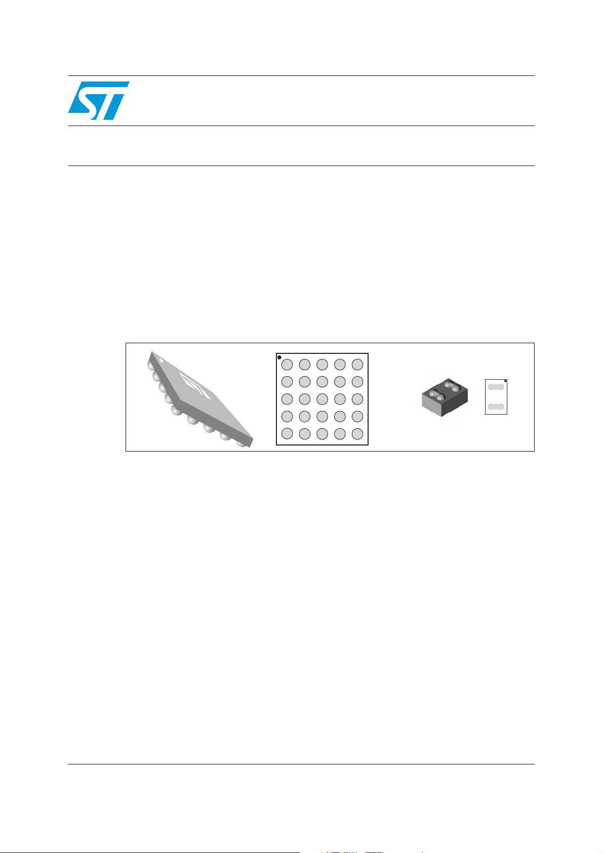
Figure 1. Typical Flip-Chip packages
Multi-bump
3
2
1
A
B
C
D
E
5
4
1
A
B
2-bar
The Flip-Chip package family has been designed to fulfil the same quality levels and the
same reliability performances as standard semiconductor plastic packages. This means
these new Flip-Chip packages should be considered as new surface mount devices which
will be assembled on a printed circuit board (PCB) without any special or additional process
steps required. In particular this package does not require any extra underfill to increase
reliability performances or to protect the device. This package is compatible with existing
pick and place equipment for board mounting. Only lead-free, RoHS compliant Flip Chips
are available in mass production.
This application note addresses the following topics:
■ Product description
■ Mechanical description
■ Packing specifications and labelling description
■ Recommended storage and shipping instructions
■ Soldering assembly recommendations
■ User responsibility and returns
■ Changes
■ Delivery quantity
■ Quality
September 2011 Doc ID 12282 Rev 4 1/17
www.st.com
Page 2
Product description AN2348
1 Product description
Flip Chips are manufactured with a wafer level process that STMicroelectronics has
developed by attaching solder bumps on I/O pads of the active wafer side, thus allowing
bumped dice to be produced. The I/O contact layout can be either matrix shape or set in
periphery. No redistribution layer is used. This allows parasitic inductances coming from the
redistribution metal tracks to be minimized.
Lead-free bump composition is 98.25% Sn, 1.2% Ag, 0.5% Cu, 0.05% Ni. This is fully
compatible with standard lead-free reflow processes. The bump dimension (255 µm bump
diameter) allows the pick and place process to be compatible with existing equipment (in
particular with equipment used for Ball Grid Array - BGA packages) and makes it also
compatible with the PCB design rules used for standard ICs.
Optional coating on the flat side of the package is available.
These components are delivered in tape and reel packing with the bumps turned down
(placed on the bottom of the carrier tape cavity). The other face of the component is flat and
allows picking as in the standard SMD packages.
Devices are 100% electrically tested before packing. The product references are marked
on the flat side of the device.
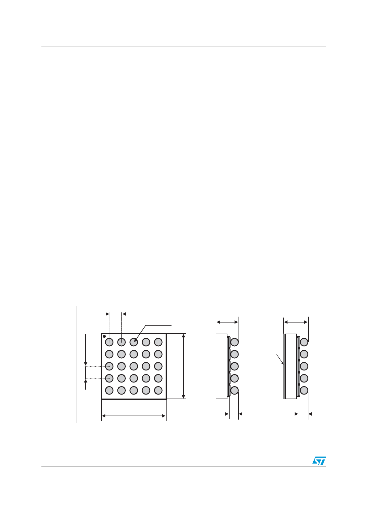
2 Mechanical description
Mechanical dimensions of Flip Chips are provided through a product example in Figure 2.
Bumps are lead-free. Bump composition is 98.25% Sn, 1.2% Ag, 0.5% Cu, 0.05% Ni alloy
with a near eutectic melting point of 218 to 227 °C. Die size and bump count are adapted to
the connection requirements.
Figure 2. Mechanical dimensions of a 5 x 5 bump matrix array (sample).
400 µm ± 40
255 µm ± 40
400 µm ± 40
1.97 mm ± 30 µm
1.97 mm ± 30 µm
605 µm ± 55
Optional
coating
200 µm ± 20 200 µm ± 20
650 µm ± 60
Note: The package height of 0.605 mm (0.650 mm for optionally coated packages) is valid for a
die thickness of 0.40 mm.
2/17 Doc ID 12282 Rev 4
Page 3
AN2348 Packing specifications and labelling description
The Flip Chip tolerance on bump diameter and bump height are very tight. This constant
bump shape insures a good coplanarity between bumps. Optical measurements performed
through vertical focuses show a bump plus die coplanarity below 50 µm.
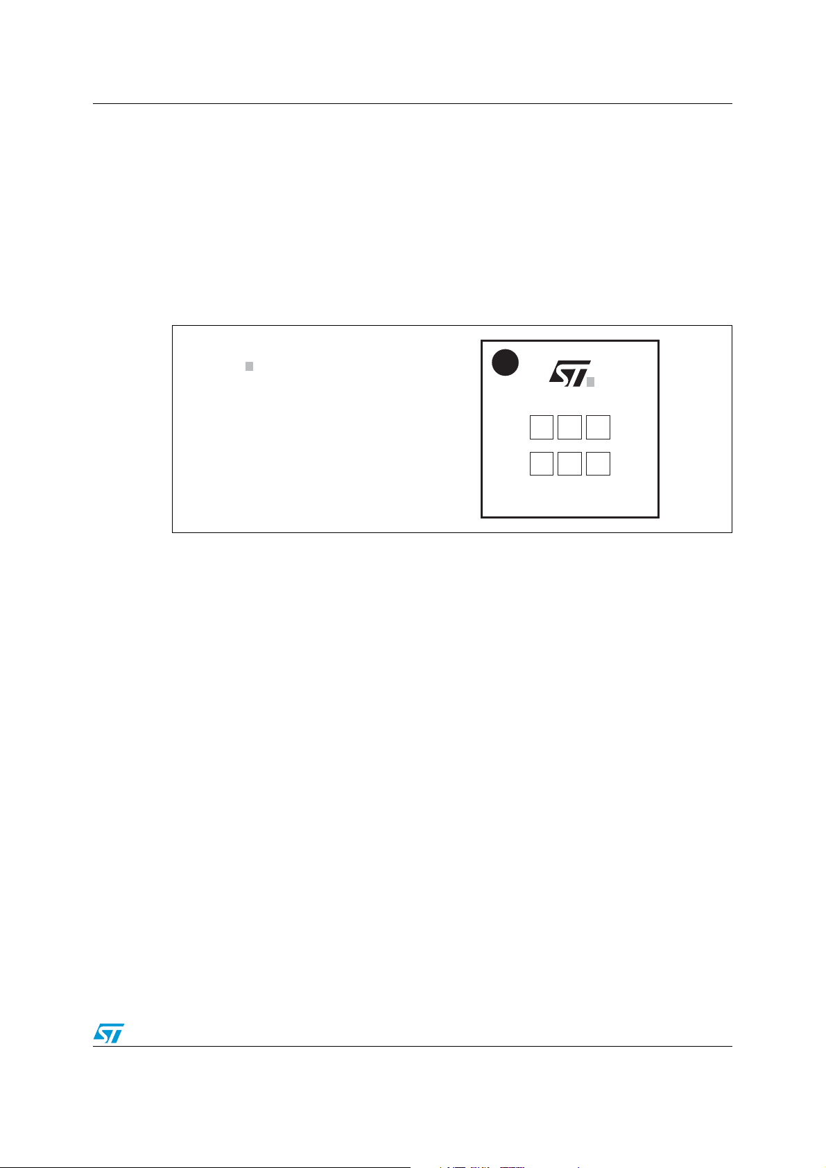
The product marking for the flat side is shown on Figure 3 (product example). The Flip Chip
has a pin marker - A1 (see Figure 1) on both the flat side and the bump side so that the
orientation of the component can be easily determined before and after assembly. The dots
marked on the flat side and on the bump side have been designed so that they can be
detected by standard vision systems.
Marking dimensions are linked to the die size.
Figure 3. Flip Chip marking example for 5x5 bump matrix array.
Dot, ST logo
ECOPACK status
xx = marking
z = manufacturing location
yww = datecode
(y = year
ww = week)
When very small die sizes leave
insufficient space, the ST logo and
ECOPACK symbol are omitted from
the marking.
xyxwz
w
3 Packing specifications and labelling description
Flip Chips are delivered in tape and reel to be fully compatible with standard high volume
SMD components. The features of tape and reel materials are in accordance with
EIA-481-D, IEC 60286-3 and EIA 763 (783) standards. All features not specified in this
section are in accordance with EIA-481-D, IEC 60286-3 and EIA 763 (783) standards.
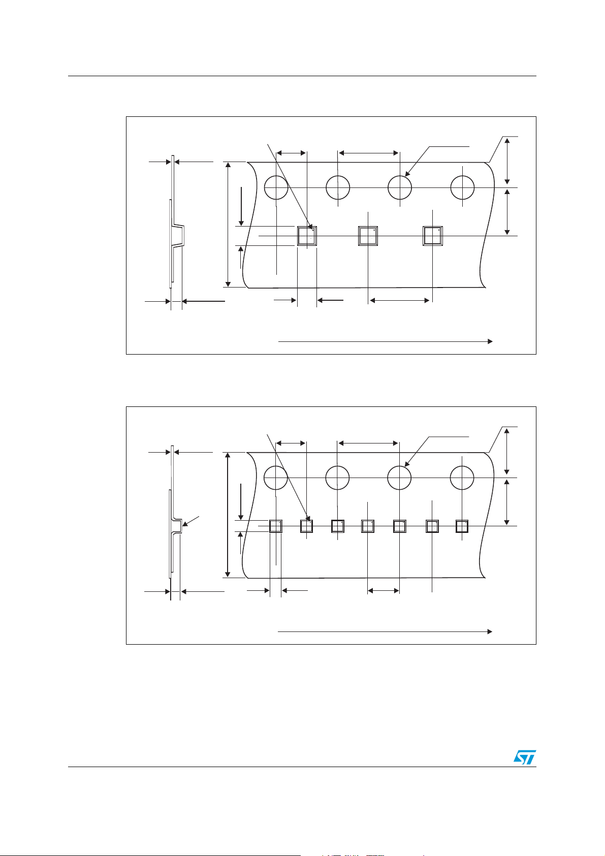
3.1 Carrier tape
Flip Chips are placed in the carrier tape with their bump side facing the bottom of the cavity
so that the components can be picked-up by their flat side. No flipping of the package is
necessary for mounting on PCB. The products are positioned in the carrier tape with pin A1
on the sprocket hole side. Carrier tape mechanical dimensions are shown in the example in
Figure 4. Standard tape width is 8 mm for die sizes smaller than 3 mm (dimension B0).
Note: 12 mm carrier tape width may be used for a larger die size to be in line with EIA standards.
Doc ID 12282 Rev 4 3/17
Page 4
Packing specifications and labelling description AN2348
Figure 4. Tape dimensions for Flip Chips greater than 0.8 x 0.8 mm
(605 µm or 505 µm thickness).
Dot identifying b ump A1 location
A1 bump location may vary with product layout
2.0
0.20
4.0
Ø 1.55
1.75
1.24
8.0
ST
ST
yww
yww
xxz
xxz
1.24
ST
yww
xxz
4.0
ST
yww
xxz
0.69 or 0.59
Typical dimensions in mm
User direction of unreeling
* A1 bump location varying with product layout
Figure 5. Tape dimensions for Flip Chips less than 0.8 x 0.8 mm
(605 µm or 505 µm or 370 µm thickness).
Dot identifying b ump A1 location
A1 bump location may vary with product layout
0.20
Cavity for
2-bar Flip Chip
has center hole
at the bottom
0.79
8.0
2.0
ST
ST
yww
yww
xxz
xxz
ST
ST
yww
yww
xxz
xxz
4.0
ST
ST
yww
yww
xxz
xxz
ST
ST
yww
yww
yww
yww
xxz
xxz
xxz
xxz
Ø 1.55
ST
ST
ST
ST
yww
yww
xxz
xxz
3.5
1.75
3.5
ST
ST
yww
yww
xxz
xxz
0.79
0.69
or 0.59
or 0.43
Typical dimensions in mm
User direction of unreeling
* A1 bump location varying with product layout
4/17 Doc ID 12282 Rev 4
2.0
Page 5

AN2348 Packing specifications and labelling description
Table 1. Tape cavity sizing
Dimension
A0 and B0 Die side size + 70 µm
smaller than or equal to 1.5 mm
The cavities in the carrier tape have been designed to avoid any damage to the
components. Specific hole is present to improve device stability during sealing and pick up
The embossed carrier tape is in a black conductive material (surface resistivity within
10E5 and 10E11 ohm/sq). Use of this material protects the component against damage
from electrostatic discharge and ensures the total discharge of the component prior to
placement on the PCB. Conductivity is guaranteed to be constant and not affected by shelf
life or humidity. The material will not break when bent and does not have any residue to rub
off, powder, or flake.
3.2 Cover tape
The carrier tape is sealed with a transparent, antistatic (surface resistivity within
10E5 ohm/sq and 10E11 ohm/sq) polyester film cover tape with a heat activated adhesive.
The cover tape tensile strength is higher than 10 N.
The peeling force of the cover tape is between 0.08 N and 0.5 N in accordance with the
testing method EIA-481-D and IEC 60286-3. Cover tape is peeled back in the direction
opposite to the carrier tape travel; the angle between the cover tape and the carrier tape is
between 165 and 180 degrees and the test is done at a speed of 120 ± 10% mm/minute.
Die with both sides
Die with one side larger than 1.5 mm
Cavity dimensions established to ensure that
component rotation cannot exceed 10° max.
Doc ID 12282 Rev 4 5/17
Page 6
Packing specifications and labelling description AN2348
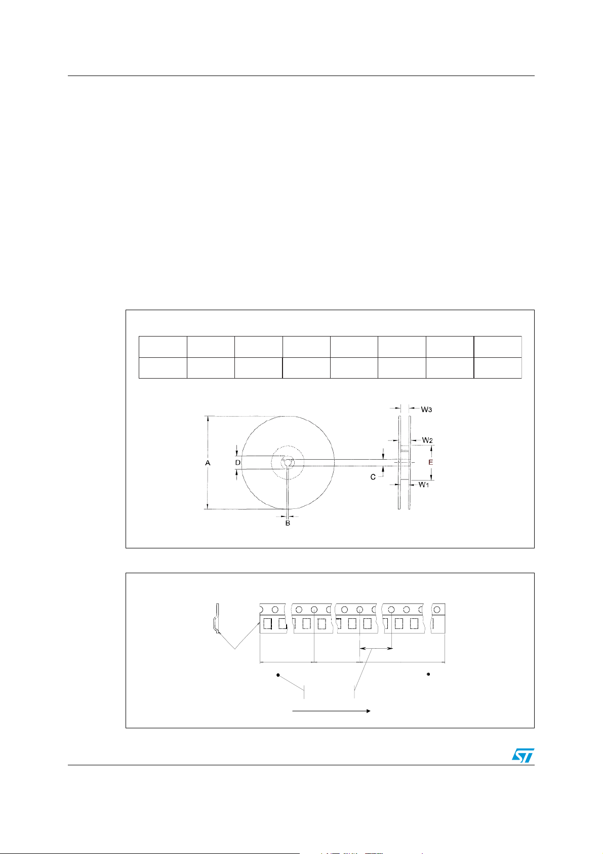
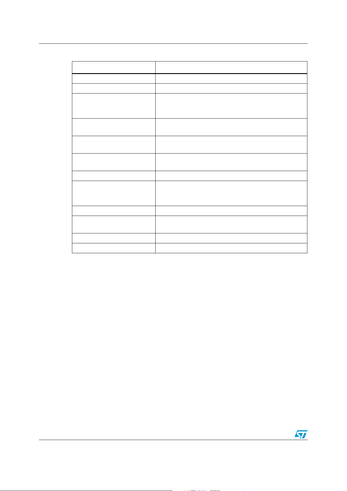
3.3 Reels
The sealed carrier tape with the Flip Chip is reeled on seven-inch reels (see Figure 6 for reel
mechanical dimensions). These reels are compliant with EIA-481-C standard. In particular,
they are made of an antistatic polystyrene material. Color of the reel may vary depending on
supplier.
Dice quantity per reel is 5000 or 10000 or 15000 (with typical package thickness equal to
600 µm). In compliance with the IEC 60286-3, each reel contains a maximum of 0.1% empty
cavities. Two successive empty cavities are not allowed. Each reel may contain components
coming from 2 different wafer lots.
Each reel has a minimum leader of 400 mm and a minimum trailer of 160 mm (compliant
with EIA 481-C and IEC 60286-3 standards). The leader makes up a portion of carrier tape
with empty cavities and sealed by cover tape at the beginning of the reel (external side). The
leader is affixed to the last turn of the carrier tape by using adhesive tape. The trailer is at
the end of the reel and consists of empty, sealed cavities (see Figure 7).
Figure 6. Seven-inch reel mechanical dimensions.
Material: ANTISTATIC POLYSTYRENE
ABCDE
180 max
All dimensions in mm
1.5 min 13
+0.5
-0.2 -0 -0.5
20.2 min
60 min
W1 (Hub)
+1.5
8.4
W2
14.4 max
W3
(external)
+2.5
8.4
Figure 7. Leader and trailer
Leader and trailer
End
No components
Top
cover
tape
Trailer
. 400mm min.
160mm min
6/17 Doc ID 12282 Rev 4
Components
Sealed with cover tape
User direction of feed
100mm min
No components
.
Leader
Start
Page 7

AN2348 Packing specifications and labelling description
3.4 Final packing
Each reel is heat sealed under inert atmosphere in a transparent, recyclable and antistatic
polyethylene bag (minimum of 4 mils material thickness).
Reels are then packed in cardboard boxes.
The complete description for packing is shown on Figure 8.
Figure 8. Packing flow chart.
dice into
the reel
3.5 Labelling
To ensure component traceability, labels are stuck on the reels and the cardboard box. The
seven inch reels and the cardboard box are identified by labels including part number,
shipped quantity and traceability references (Figure 9).
The traceability is ensured for each production lot and each shipment lot through the
labeling.
The trace code number printed on the labels ensures backward traceability from the lot
received by the customer at each step of the process - in / out dates and quantity at
diffusion, assembly, test and final store. Likewise, forward traceability is able to trace a lot
history from the wafer fab to the customer’s location.
Figure 9. Example of a reel label
Reel in a sealed
plastic bag within
inert atmosphere
The reel in its bag is packed in a
cardbox for storage & shipment
Doc ID 12282 Rev 4 7/17
Page 8
Packing specifications and labelling description AN2348
Table 2. Parameter reel label
Field Field type
Assembled in Mandatory-Country of origin
Pb-free 2nd. Level interconnect As per JEDEC Standard JESD97
Mandatory for concerned products as defined in MPI
MSL
Bag seal date
PBT
Category
Eco level Mandatory for ECOLEVEL devices only as defined in MPI
Ty p e
Total qty Mandatory - bulk quantity
Moisture Sensitivity Level as per JEDEC J-STD-020
Mandatory for SMD
For MSL 2 and above, date of vacuum sealing of dry bag
For MSL=1, “Not Moisture Sensitive” must be printed instead
Peak Package Body Temperature as JEDEC J-STD-020
Mandatory for the SMD
Pb-free category as pr JEDEC Standard JESD97
Mandatory for concerned products as defined in MPI
Mandatory
First line: Not Required
Second line: Raw line product name
Trace code
MandatoryTraceability code with Wafer Fab Production Area Code
Bulk ID Mandatory- Bulk ID Number, Start with A
Bar code Mandatory-Bar code area
8/17 Doc ID 12282 Rev 4
Page 9

AN2348 Recommended storage, shipping instructions and descriptions
4 Recommended storage, shipping instructions and
descriptions
Flip-Chip reels are packed under inert N2 atmosphere in a sealed bag. For shipment and
handling, reels are packed in a cardboard box.
STMicroelectronics thus recommends the following shipping and storage conditions:
● relative humidity between 15% and 70%
● temperature range from -55 °C to +150 °C
Components in a non opened sealed bag can be stored 6 months after shipment.
Components in tape and reel must be protected from exposure to direct sunlight.
Moisture sensitivity level (MSL as per JEDEC J-STD-020C) is not applicable to Flip-Chip
devices since there is no plastic encapsulation and so no risk of moisture absorption and
related possible package cracks.
Doc ID 12282 Rev 4 9/17
Page 10
Soldering assembly recommendations AN2348
5 Soldering assembly recommendations
5.1 PCB design recommendations for multi-bump Flip Chips
For optimum electrical performance and highly reliable solder joints, STMicroelectronics
recommends the PCB design guidelines listed in Table 3..
Table 3. PCB design recommendations.
PCB pad design
PCB pad size Ø = 260 µm max. (circular) - 220 µm recommended
Solder mask opening Ø = 300 µm min. (for 260 µm diameter pad)
PCB pad finishing Cu - Ni (2-6 µm) - Au (0.2 µm max) or Cu OSP (Organic Substrate Protection)
Note: A too thick gold layer finishing on the PCB pad is not recommended (low joint reliability).
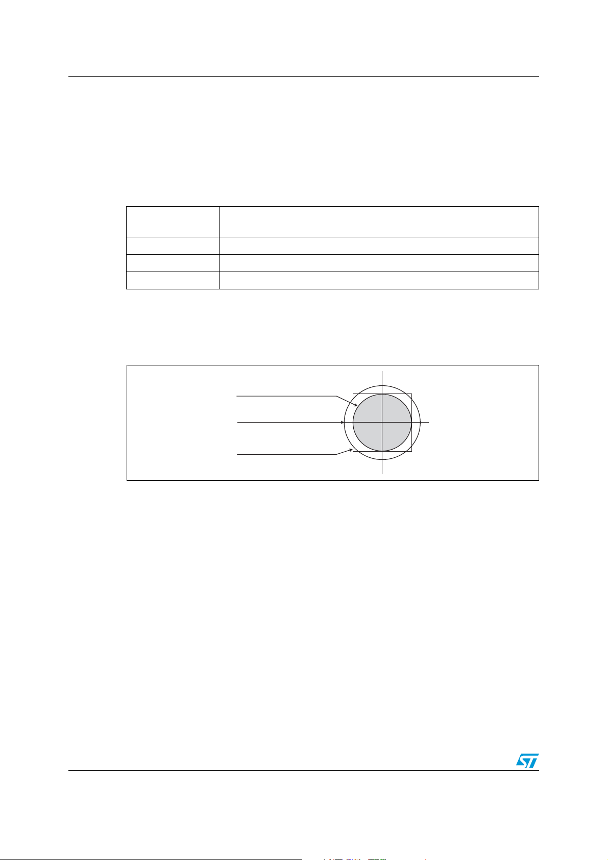
To optimize the natural self centering effect of Flip Chips on PCB, PCB pad positioning and
size have to be properly designed (see Figure 10).
Figure 10. Multi-bump Flip-Chip bump footprint
Non Solder Mask Defined
Micro via under bump allowed
Copper pad Diameter:
220 µm recommended
260 µm maximum
Solder mask opening:
300 µm minimum
Solder stencil opening :
220 µm recommended
Micro vias
An alternative to routing on the top surface is to route out on buried layers. To achieve this,
the pads are connected to the lower layers using micro vias.
10/17 Doc ID 12282 Rev 4
Page 11
AN2348 Soldering assembly recommendations
5.2 PCB design recommendations for 2-bar Flip Chips
For optimum electrical performance and highly reliable solder joints, STMicroelectronics
recommends the PCB design recommendations listed in Ta bl e 4 .
Table 4. PCB design recommendations for solder bar pitch 400 µm
Oblong pad: 370 x 180 µm
– Micro via SSBU allowed
– Micro via SBU to be avoided
For NSMD PCB
non solder mask defined
For SMD PCB
solder mask defined
PCB Pad Finishing Cu – Ni (2-6 µm) - Au (0.2 µm max)
– Micro via SBU filled (under qualification)
Tr a ck :
– Only one track per pad
– Maximum track width = 100 µm
Track layout must be symmetrical to the die axis (to homogenize stress
and welding attraction during reflow assembly)
Oblong pad:
– Micro via SSBU allowed
– Micro via SBU to be avoided
– Micro via SBU filled (under qualification)
Note: A gold layer finishing on the PCB pad that is too thick (0.2 µm maximum) is not
recommended (low joint reliability).
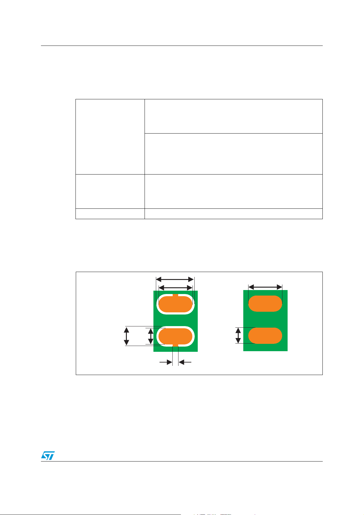
To optimize the natural self centering effect of CSP on the PCB, PCB pad positioning and
size have to be properly designed (see Figure 11).
Figure 11. Solder mask opening
450 µm
370 µm
Solder mask defined
255 µm
370 µm
180 µm
Non solder mask defined
180 µm
100 µm
Micro vias
An alternative to routing on the top surface is to route out on buried layers. To achieve this,
the pads are connected to the lower layers using micro vias. Only SSBU via technology is
approved.
Doc ID 12282 Rev 4 11/17
Page 12
Soldering assembly recommendations AN2348
5.3 PCB assembly guidelines
For Flip Chip mounting on the PCB, STMicroelectronics recommends the use of a solder
stencil aperture of 330 x 330 µm
2
maximum and a typical stencil thickness of 125 µm.
Flip Chips are fully compatible with the use of near eutectic 95.8% Sn, 3.5% Ag, 0.7% Cu
solder paste with no-clean flux. ST's recommendations for Flip-Chip board mounting are
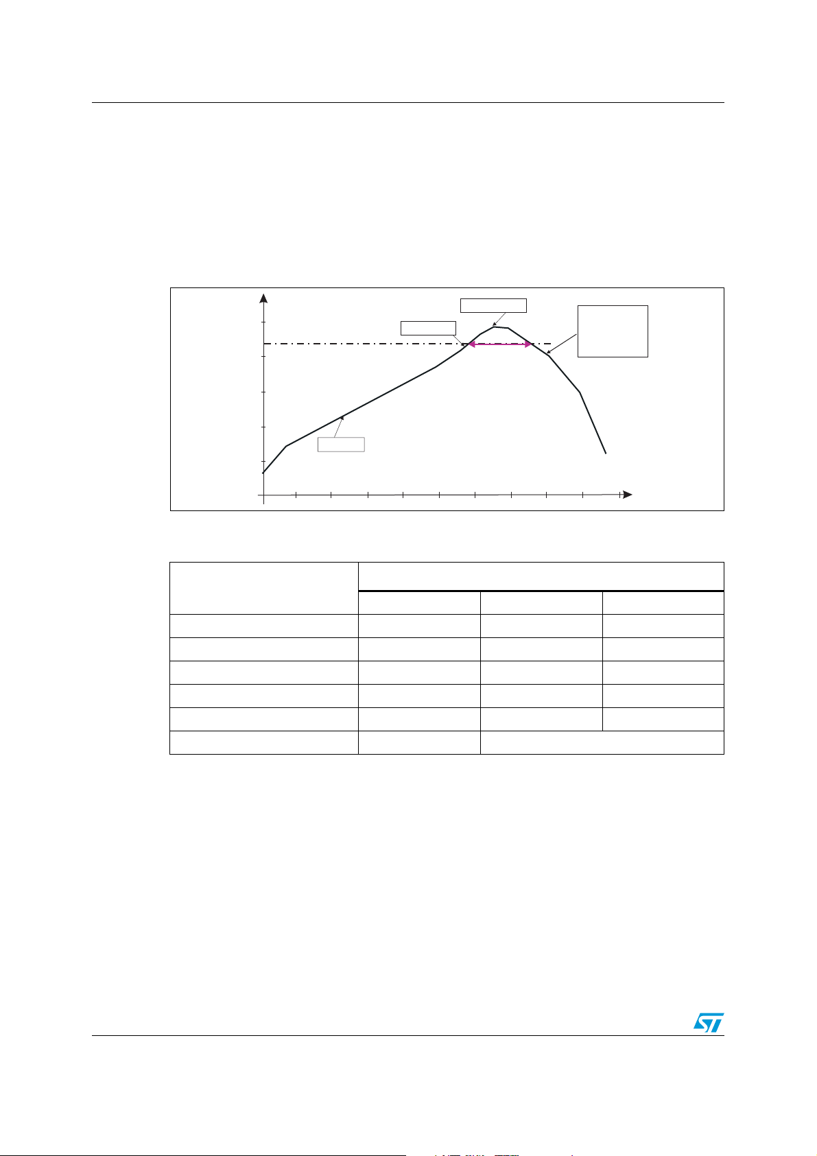
illustrated on the soldering reflow profile shown in Figure 12.
Figure 12. ST ECOPACK
®
recommended soldering reflow profile for Flip Chip
mounting on PCB (definitions)
250
250
250
250
0.9 °C/s
250
0
Table 5. ST ECOPACK
240-245 °C
2 - 3 °C/s
60 sec
(90 max)
®
recommended soldering reflow profile for Flip Chip
-2 °C/s to
-3 °C/s
-6 °C/s max
240210180150120906030 300
270
mounting on PCB (value)
Profile Ramp to strike
Typical Max.
Temp. gradient in preheat (T = 70 – 180 °C) 0.9 °C/s 3 °C/s
Temp. gradient (T = 200 – 225 °C) 2 °C/s 3 °C/s
Peak temp. in reflow 240 - 245 °C 260 °C
Time above 220 °C 60 s 90 s
Temp. gradient in cooling -2 to - 3 °C/s -6 °C/s
Time from 50 to 220 °C 160 to 220 s
Dwell time in the soldering zone (with temperature higher than 220 °C) has to be kept as
short as possible to prevent component and substrate damages. Peak temperature must not
exceed 260 °C. Controlled atmosphere (N
or N2H2) is recommended during the whole
2
reflow, specially above 150 °C.
Flip Chips are able to withstand three times the previous recommended reflow profile to be
compatible with a double reflow when SMDs are mounted on both sides of the PCB plus one
additional repair.
A maximum of three soldering reflows are allowed for these lead-free packages (with repair
step included).
The use of a no-clean paste is highly recommended to avoid any cleaning operation. To
prevent any bump cracks, ultrasonic cleaning methods are not recommended.
12/17 Doc ID 12282 Rev 4
Page 13

AN2348 Soldering assembly recommendations
5.4 Underfilling
Underfilling is not essential for Flip Chips. These devices can do without an underfill if the
process temperature does not exceed 175 °C and if the process time is short (typically 5
minutes).
5.5 Manual rework
Flip Chips are able to tolerate one repair in addition to the two reflows mentioned in
Section 5.3.
As for other BGA type packages the use of laser systems is the most suitable form for
Flip Chip repair. Manual hot gas soldering is acceptable but iron soldering is not
recommended.
For leaded Flip Chip manual rework the maximum temperature allowed is 260 °C (lead-free
compatibility) and dwell time must not exceed 30 seconds.
For lead-free Flip Chip manual rework, the maximum temperature allowed is 260 °C. The
typical soldering profile of Figure 12 can be used.
5.5.1 Rework procedure
Remove the device
Rework process start with the removal of the device. To remove the device, heat must be
applied to melt the solder joints so that the component can be lifted from the board.
Large area bottom side preheaters may be used to raise the temperature of the board. This
may help to minimize warping of the board, and minimize the amount of heat that must be
applied on the component.
Top heating may be applied to the component by using a laser or a convective hot gas
nozzle. Nozzle size must be selected to match the component footprint appropriately. After
top heating has melted the solder, vacuum is applied through the pick-up nozzle, and the
component is lifted from the board.
The heat should be carefully directed at the component to be removed to avoid adjacent
components solder joints being reflowed. Shielding, control of gas flow from the nozzle, and
accurate temperature control are the key parameters.
Removing solder
Next step is cleaning the solder from the work site. Due to space constraints and the need
for accurate temperature control, automatic tools are recommended.
Typically, site cleaners consist of controlled non-contact gas heating and vacuuming tools.
The objective is to remove the residual solder from the site without damaging the pads,
solder masks or adjacent components, and to prepare the site for application of new
component.
Doc ID 12282 Rev 4 13/17
Page 14

Soldering assembly recommendations AN2348
New device soldering
For placement of the device several solutions are possible:
● Use a mini-stencil and solder paste then place the device. This is the preferred solution
to ensure homogeneity of assembly conditions if assembly of WLCSP (wafer level chip
scale package) is performed with solder paste, even if small footprints and tight
dimensions make this operation difficult.
● Use no-clean flux on the site and place the device.
● Dip the WLCSP in no-clean flux, and to place it on the board.
Next operation is to reflow the solder joint by applying controlled heat to the component.
This can be done in much the same way as described above for component removal, but
accurate temperature control is necessary to ensure good soldering of the joint.
Alternatively this can be done by putting the whole board in a furnace. See Figure 12 for
reflow profile recommendations.
Equipment
Systems for these operations are available at various levels of automation. Methods and
techniques used in more sophisticated automatic systems can be copied using manual
equipment. Soldering irons should be avoided for these operations. Tweezers or any picking
tools pressuring the sides or bottom (bump side) of the WLCSP must be avoided since such
tools can damage silicon and create chip outs.
Figure 13 shows an example of semi-automatic equipment for component rework. (See the
Web site of Comintec for more information.)
Figure 13. Comintec ONYX32 - Semi-automatic equipment for component rework
14/17 Doc ID 12282 Rev 4
Page 15

AN2348 Changes
ONYX32 Key Features
● Fully automated X,Y,Z and theta control
● Fully automated alignment using digital feature separation (DFS) technology
● Precision force sensor and mass flow controller
● Four zone bottom preheater
● Flux dipping station
● FireWire (IEEE 1394) controls
● Visual machines software
● Machine table including power supply cabinet
ONYX32 Options
● Dispensing head for solder paste, flux, underfill or adhesives
● Non-contact temperature sensor
● Site solder removal system
6 Changes
STMicroelectronics reserves the right to implement minor changes of geometry and
manufacturing processes without prior notice. Such changes will not affect electrical
characteristics of the die, the pad layout or the maximum die size. However for confirmed
orders, no variation will be made without customer’s approval.
7 Quality
7.1 Electrical inspection
Products in Flip Chip are 100% electrically probed according to the critical parameters of the
ST product specification. The last operation before packing is 100% electrical testing. The
other parameters are guaranteed by technology, design rules and by continuous monitoring
systems.
7.2 Visual inspection
A visual control is performed on all manufacturing lots according to the MIL-STD-883
method 2010.
Doc ID 12282 Rev 4 15/17
Page 16

Conclusion AN2348
8 Conclusion
Lead-free Flip-Chip packages have been developed by STMicroelectronics for electronic
applications where integration and performance are the main concerns of designers.
STMicroelectronics Flip Chips offer:
● Remarkable board space saving (package size equal to die size and total height less
than 605 µm)
● Enhanced electrical performance (minimized parasitic inductance due to very short
electrical paths and absence of redistribution layer)
● High reliability due to integration of a whole function traditionally based on discrete
interconnected components.
Flip Chips are delivered in tape and reel and are fully compatible with other high volume
SMD components (standard plastic packages or CSP/BGA packages) regarding existing
pick and place equipment, standard solder reflow assembly equipment and standard PCB
techniques.
9 Revision history
Table 6. Document revision history
Date Revision Changes
15-Sep-2006 1 First issue
15-Oct-2006 2 Added section 5.4.1 on Rework procedure.
Updated bump composition in Section 1: Product
10-Mar-2010 3
06-Sep-2011 4
description and Section 2: Mechanical description.
Updated solder paste composition in Section 5.3: PCB
assembly guidelines. Updated for 2-bar Flip Chips.
Updated references to standards. Added parameter
variations for tape dimensions in Figure 4 and Figure 5.
Added Figure 7. Updated reel label in Figure 9. Updated
soldering reflow profile in Figure 12.
16/17 Doc ID 12282 Rev 4
Page 17

AN2348
Please Read Carefully:
Information in this document is provided solely in connection with ST products. STMicroelectronics NV and its subsidiaries (“ST”) reserve the
right to make changes, corrections, modifications or improvements, to this document, and the products and services described herein at any
time, without notice.
All ST products are sold pursuant to ST’s terms and conditions of sale.
Purchasers are solely responsible for the choice, selection and use of the ST products and services described herein, and ST assumes no
liability whatsoever relating to the choice, selection or use of the ST products and services described herein.
No license, express or implied, by estoppel or otherwise, to any intellectual property rights is granted under this document. If any part of this
document refers to any third party products or services it shall not be deemed a license grant by ST for the use of such third party products
or services, or any intellectual property contained therein or considered as a warranty covering the use in any manner whatsoever of such
third party products or services or any intellectual property contained therein.
UNLESS OTHERWISE SET FORTH IN ST’S TERMS AND CONDITIONS OF SALE ST DISCLAIMS ANY EXPRESS OR IMPLIED
WARRANTY WITH RESPECT TO THE USE AND/OR SALE OF ST PRODUCTS INCLUDING WITHOUT LIMITATION IMPLIED
WARRANTIES OF MERCHANTABILITY, FITNESS FOR A PARTICULAR PURPOSE (AND THEIR EQUIVALENTS UNDER THE LAWS
OF ANY JURISDICTION), OR INFRINGEMENT OF ANY PATENT, COPYRIGHT OR OTHER INTELLECTUAL PROPERTY RIGHT.
UNLESS EXPRESSLY APPROVED IN WRITING BY TWO AUTHORIZED ST REPRESENTATIVES, ST PRODUCTS ARE NOT
RECOMMENDED, AUTHORIZED OR WARRANTED FOR USE IN MILITARY, AIR CRAFT, SPACE, LIFE SAVING, OR LIFE SUSTAINING
APPLICATIONS, NOR IN PRODUCTS OR SYSTEMS WHERE FAILURE OR MALFUNCTION MAY RESULT IN PERSONAL INJURY,
DEATH, OR SEVERE PROPERTY OR ENVIRONMENTAL DAMAGE. ST PRODUCTS WHICH ARE NOT SPECIFIED AS "AUTOMOTIVE
GRADE" MAY ONLY BE USED IN AUTOMOTIVE APPLICATIONS AT USER’S OWN RISK.
Resale of ST products with provisions different from the statements and/or technical features set forth in this document shall immediately void
any warranty granted by ST for the ST product or service described herein and shall not create or extend in any manner whatsoever, any
liability of ST.
ST and the ST logo are trademarks or registered trademarks of ST in various countries.
Information in this document supersedes and replaces all information previously supplied.
The ST logo is a registered trademark of STMicroelectronics. All other names are the property of their respective owners.
© 2011 STMicroelectronics - All rights reserved
STMicroelectronics group of companies
Australia - Belgium - Brazil - Canada - China - Czech Republic - Finland - France - Germany - Hong Kong - India - Israel - Italy - Japan -
Malaysia - Malta - Morocco - Philippines - Singapore - Spain - Sweden - Switzerland - United Kingdom - United States of America
www.st.com
Doc ID 12282 Rev 4 17/17
 Loading...