

Page 1

AN2340
Application note
ST10 RPD pin: Functionality during Reset and Power Down mode
Introduction
RPD is a dedicated timing pin for the return from Power Down circuit. Additionally, when this
pin is recognized low, a reset event is taken as asynchronous. This note gives advice on
configuring the external circuitry connected to the RPD in order to make it work properly.
The information contained in this document is valid for ST10F27x, ST10R27x, ST10F25x
and ST10F296.
March 2006 Rev 1 1/10
www.st.com
Page 2
RPD functionality AN2340
1 RPD functionality
RPD is a dual purpose dedicated pin. This section covers its functionality.
1.1 System reset and startup
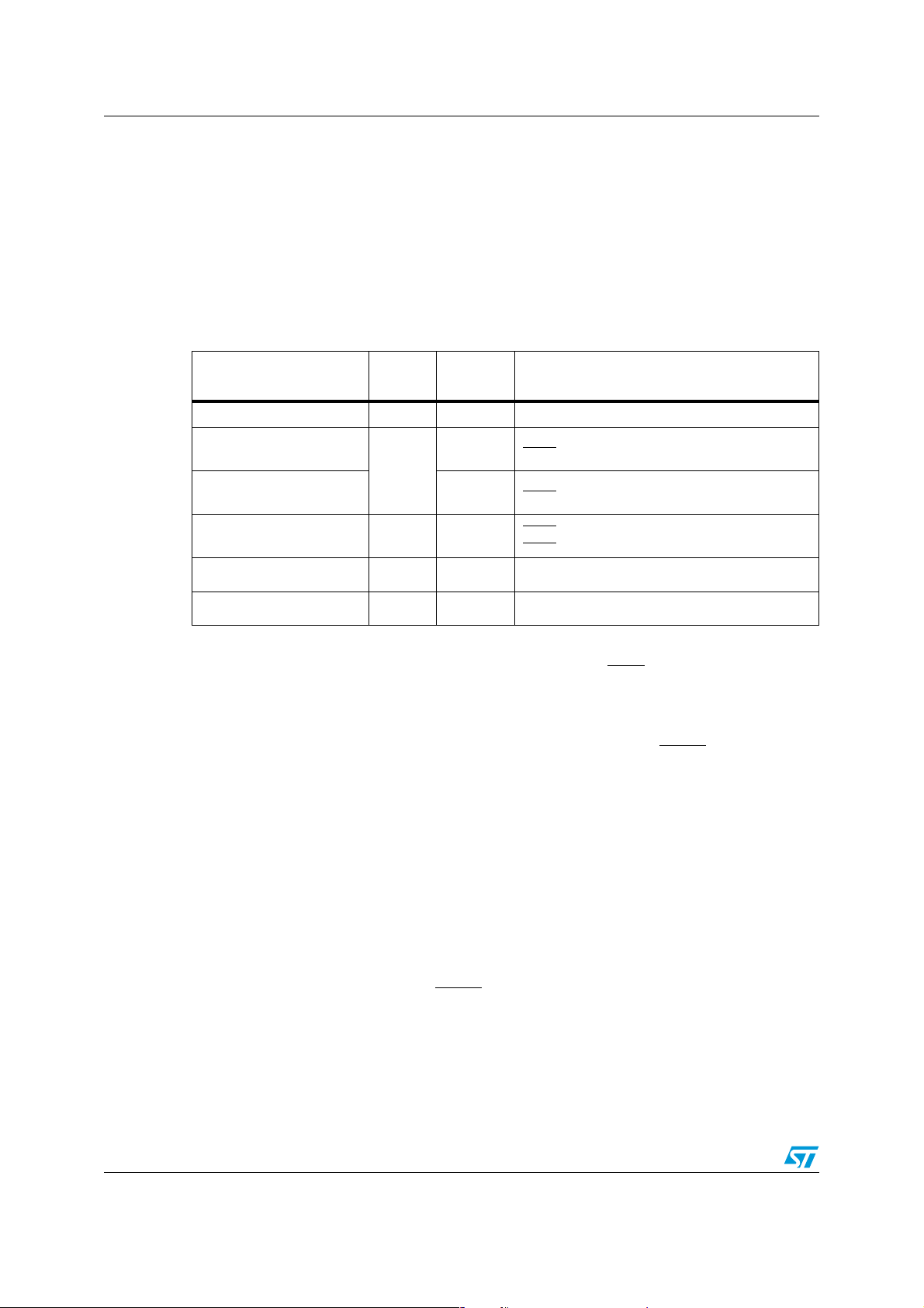
Several ST10 reset events that may occur are summarized in the following table:
Table 1. Reset event definition
Reset Source Flag
Power-on reset PONR Low Power-on
Asynchronous hardware
reset
Synchronous long
hardware reset
Synchronous short
hardware reset
Watchdog timer reset WDTR
Software reset SWR
1. Flags can be read in the WDTCON register
2. The RPD status has no influence unless Bidirectional Reset is activated (bit BDRSTEN in SYSCON): RPD
low inhibits the Bidirectional reset on SW and WDT reset events, that is RSTIN
(1)
LHWR
SHWR High
RPD
Status
Low t
High t
(2)
(2)
Conditions
> 500ns
RSTIN
> (1032 + 12) TCL + max (4 TCL, 500ns)
RSTIN
> max (4 TCL, 500ns)
t
RSTIN
≤ (1032 + 12) TCL + max (4 TCL, 500ns)
t
RSTIN
WDT overflow
SRST instruction execution
is not activated.
Therefore, roughly, the RPD pin level distinguishes between an asynchronous (low level)
and a synchronous reset (high level). The main difference between these two kinds of reset
is that the first immediately cancels pending internal hold states and if any, it aborts all
internal/external bus cycles whereas in the synchronous reset, after RSTIN
level is
detected, a short duration of a maximum of 12 TCL (six periods of CPU clock) elapses,
during which pending internal hold states are cancelled and the current internal access
cycle, if any , is completed. For this reason, if an asynchronous reset occurs during a read or
write phase in internal memories, the content of the memory itself could be corrupted. To
avoid this, synchronous reset usage is strongly recommended.
However, the asynchronous reset must be used during the power-on of the device.
Depending on crystal or resonator frequency, the on-chip oscillator needs about 1ms to
10ms to stabilize with an already stable V
stabilized clock signal to detect an asynchronous reset and is therefore suitable for poweron conditions.
On the contrary, the reset state machine needs a stabilized clock to operate correctly.
According to the length of pulse on RSTIN
2/10
. The logic of the ST10 does not need a
DD
, the synchronous reset may be recognized as
Page 3
AN2340 RPD functionality
long or short. Long and Short synchronous reset differs by the start-up configuration bits
latched:
– Long synchronous reset latches the entire Port0 configuration, including clock
frequency selection (P0[15:13])
– Short synchronous reset ignores the bits P0[15:13] and the same clock frequency
is applied.
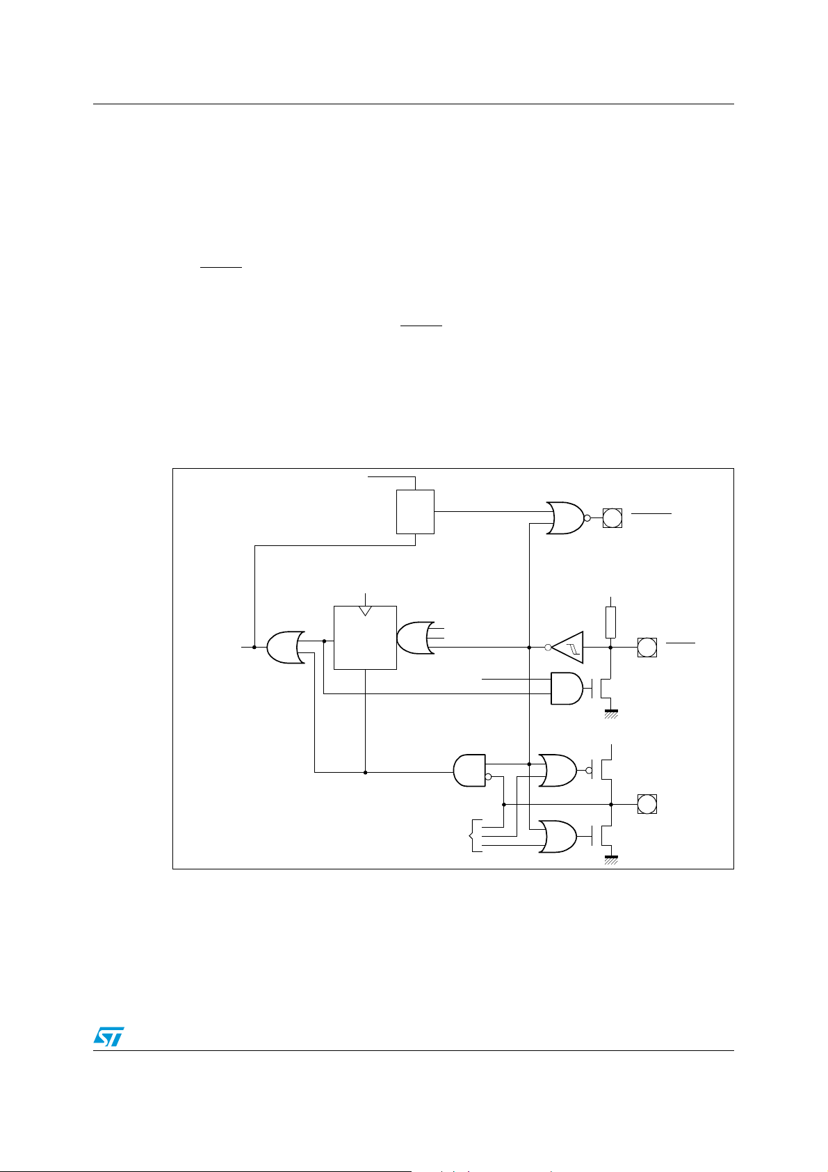
Refer to the product documentation for a full description of the reset mechanism.
The RSTIN
pin is an input of the device that can be configured as output that shows a low
level during the internal reset condition. This is called the bidirectional reset and is enabled
by setting the BDRSTEN bit in the SYSCON register.
When enabled, the open drain of the RSTIN
pin is activated, pulling down the reset signal
for the duration of the internal reset sequence (synchronous/asynchronous hardware,
synchronous software and synchronous watchdog timer resets). At the end of the internal
reset sequence (1024 TCL) the pull-down is released.
The figure below shows a simplified reset circuitry scheme.
Please refer to the product user
manual for more details and timings related to system reset.
Figure 1. Internal (simplified) reset circuitry
EINIT instruction
Clr
Internal
reset
signal
Reset state
machine
Clock
Trigger
Clr
Q
Set
SRST instruction
watchdog overflow
Reset sequence
(512 CPU Clock Cycles)
BDRSTEN
V
RSTOUT
DD
RSTIN
V
DD
Asynchronous
reset
RPD
From/to exit
powerdown
circuit
Weak pull- down
(~200µA)
3/10
Page 4

RPD functionality AN2340
1.2 Power down
To reduce power consumption, the microcontroller can be switched to Power Down mode.
Clocking of all internal blocks is stopped, the contents of the internal RAM, however, are
preserved through the voltage supplied via the V
The ST10 pr ovides two different operating Power Down modes:
● Protected Power Down mode
● Interruptible Power Down mode
The Power Down operating mode is selected by the bit PWDCFG in the SYSCON register.
pins (and on-chip voltage regulator).
DD
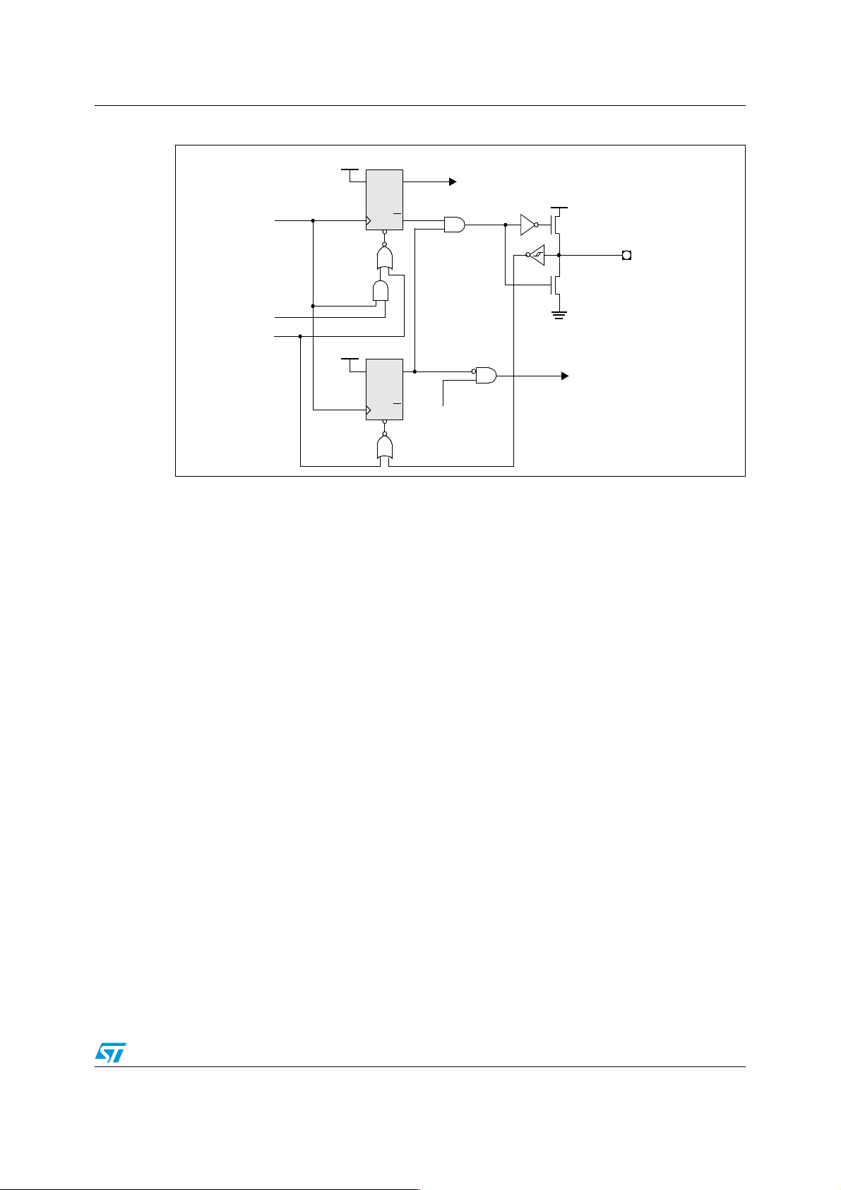
In the first case, the Power Down mode can only be entered if the NMI
(Non Maskable
Interrupt) pin is externally pulled low while the PWRDN instruction is executed and the only
way to exit the Power Down mode is with an external hardware reset.
In the second case, the Pow er Down mode can be entered if enabled Fast External Interrupt
pins (EXxIN pins, alternate functions of Port 2 pins, with x = 7...0) are in their inactive level.
This inactive level is configured with the EXIxES bit field in the EXICON register, as follows:
EXICON (F1C0H / E0H) ESFR Reset value: 0000H
1514131211109876543210
EXI7ES EXI6ES EXI5ES EXI4ES EXI3ES EXI2ES EXI1ES EXI0ES
RW RW RW RW RW RW RW RW
Bit Function
External Interrupt x Edge Selection Field (x=7...0)
‘00’: Fast external interrupts disabled: Standard mode.
EXxIN pin not taken into account for entering/exiting Power Down mode.
‘01’: Interrupt on positive edge (rising).
i
EXIxES
(x=7...0)
Enter Power Down mode if EX
active level)
‘10’: Interrupt on negative edge (falling).
Enter Power Down mode if EX
active level)
‘11’: Interrupt on any edge (rising or falling).
Always enter Power Down mode, exit if EXxIN level changed.
IN = ‘0’, exit if EXxIN = ‘1’ (referred to as ‘high’
i
IN = ‘1’, exit if EXxIN = ‘0’ (referred to as ‘low’
Interruptible Power Down mode can be exited by asserting either RSTIN or one of the
enabled EXxIN pins (Fast External Interrupt).
4/10
Page 5
AN2340 RPD functionality
Figure 2. Simplified power down exit circuitry
V
DD
en_clk_n
stop PLL
stop oscillator
exit_pwrd
V
DD
Pull-Up
Weak pull-down
(~ 200 µA)
CPU and peripherals clocks
RPD
Enter
Power Down
External
interrupt
Reset
DQ
Q1
cd
V
DD
DQ
Q2
cd system clock
Q
Q
5/10
Page 6

External RPD circuitry examples AN2340
2 External RPD circuitry examples
To ensure that both functions explained in the previous chapter work correctly, external
circuitry must be connected to the RPD.
2.1 RC network
A simple RC network can be connected to the RPD pin leading to correct behavior both
during system reset and return from power down. The cases will be analyzed separately
considering that the resi st anc e R and the capacito r C are connec ted as in
2.1.1 System reset
On power-up, the logical low level on the RPD pin forces an asynchronous hardware reset
when
RSTIN
is asserted low (see
capacitor C. Note that an internal pull-down device on the RPD pin is turned on when the
RSTIN
pin is low, and causes the external capacitor (C) to begin discharging at a typical rate
of 100 to 200µA. With this mechanism, after a power-up reset, short low pulses applied on
RSTIN
produce synchronous hardware reset. If
needed for C to be discharged by the internal pull-down device, then the device is forced
into an asynchronous reset.
Figure 1
). The external pull-up R will then charge the
RSTIN
is asserted longer than the time
Figure 3
.
2.1.2 Return from power down
To exit Pow er Down mode with external interrupt, an EXxIN pin must be asserted for at least
40ns (x = 7...0). This signal enables the internal main oscillator (if not already running) and
PLL circuitry, and also turns on the internal weak pull-down on RPD pin. The discharging of
the external capacitor C provides a delay that allows the oscillator and PLL circuits to
stabilize before the internal CPU and Peripheral clocks are enabled. When the voltage on
the RPD pin drops below the threshold voltage, the CPU and Peripheral clocks are enabled
and the device resumes code execution (see
Figure 3. RPD pin: Internal (simplified) and external circuitry
Driven by internal
reset/pwrnd
circuitry
Figure 2 on page 5
V
DD
Pull-Up
RPD
Weak Pull-Down
(~ 200 µA)
).
V
DD
R
+
C
6/10
Page 7
AN2340 External RPD circuitry examples
2.1.3 RC network sizing
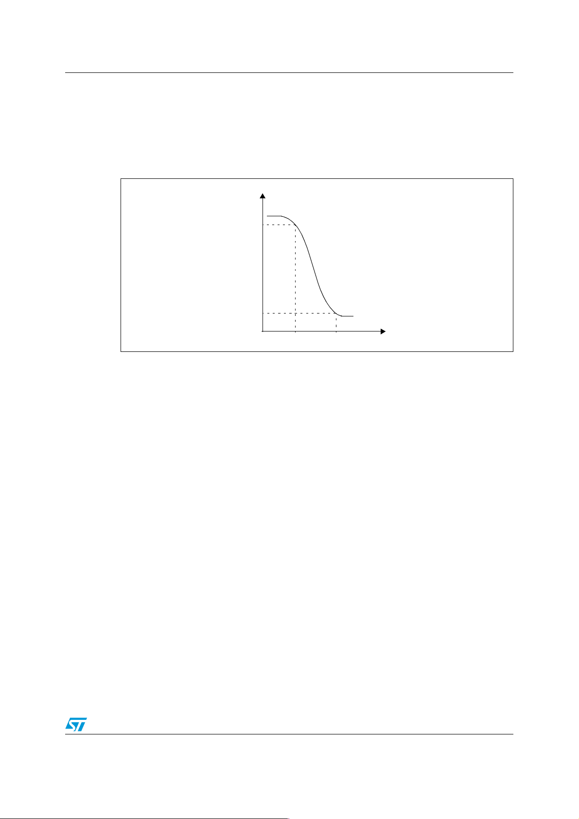
To calculate the external C value, we will suppose that a time T is required to stabilize the
oscillator and PLL circuit. Regarding a generic inverter I/O characteristic, the output level V
of that inverter can be considered high as long as the input level V
(see
Figure 4: Generic inverter I/O characteristics
).
Figure 4. Generic inverter I/O characteristics
V
o
V
OHmin
V
OLmax
V
ILmax
V
IHmin
is higher than its V
i
V
i
IHmin
o
In the same way, as long as RPD voltage is higher than V
fed with any clock (
Figure 2: Simplified power down exit circuitry
value must be chosen to maintain the voltage above V
required by PLL and the oscillator (also input hysteresis on RPD pin V
, CPU and peripherals are not
IH1
). Therefore, the capacitor
for at least the time T
IH1
HYS4
must be
restart
considered).
Using the simple formula that controls the discharge of capacitor C, we obtain:
I
pulldownTrestart⋅
C
------------ ------------- ------------ ----------- ------------- ----=
where I
pulldown
Supposing V
V
HYS4max
= 1500 mV, I
VDD V
is the current that flows internally through the weak pull-down.
= 5V, since (see product datasheet) V
DD
pulldown
= 200µA and T
–()–
IH1VHYS4
= 3.5V, V
IH1
= 10.2ms (crystal oscillator + PLL),
restart
HYS4min
= 500 mV,
it follows:
I
C
pulldownTrestart⋅
------------- ------------- ------------ ----------- ------------- ------------ --
VDD V
–()–
IH1VHYS4min
6–
⋅⋅ ⋅
200 10
------------ ------------- ------------- ---------- ------------- ---------
10 2, 10
2
3–
1µF∼==
As during reset a pull-down is activated on the RPD pin, the capacitor C will be discharged.
Subsequently the voltage will drop, causing the RPD pin to be seen at a low level. Therefore,
an asynchronous reset will be detected.
7/10
Page 8

External RPD circuitry examples AN2340
Table 2 .
RSTIN
pulse length and reset events in presence of an RC network
Pulse length Event
t
<= 500ns No effect (filtered)
RSTIN
500ns < t
512 CPU clock cycles < t
t
> 10ms Asynchronous reset
RSTIN
< 512 CPU clock cycles Short synchronous reset
RSTIN
< 10ms Long synchronous reset
RSTIN
The value of the resistance R, instead, is linked to the time needed to charge the capacitor
C. Normally 220KΩ < R < 1MΩ
.
2.2 Alternate configuration
If both synchronous reset and interruptible power down modes are not required, it is
possible to connect the RPD pin to ground, directly or through a resistance.
Figure 5. RPD pin connected to ground
V
DD
Pull-Up
driven by internal
reset/pwrnd
circuitry
Weak Pull-Down
(~ 200 µA)
RPD
The internal pull-up is sized to allow a direct connection to ground without any problem to
the internal circuitry.
As already explained, with this kind of connection, any pulse longer than 500ns on the
RSTIN
pin leads to an asynchronous reset. Moreover, it is not advised to use an interruptible
power-down.
8/10
Page 9

AN2340 Revision history
3 Revision history
Table 3. Document revision history
Date Revision Changes
30-Mar-2006 1 Initial release.
9/10
Page 10

AN2340
Please Read Carefully:
Information in this document is provided sole ly in connecti on with ST produ cts. STMicro electroni cs NV and its subsi diaries (“ST ”) reserve the
right to make changes , cor recti ons , modif ic ations or improv ement s, t o th is documen t, and the prod ucts an d servic es des crib ed he rein a t any
time, without notice.
All ST products are sold pursuant to ST’s terms and conditions of sale.
Purchasers are solely responsible for the choice, selection and use of the ST products and services described herein, and ST assumes n o
liability whatsoever relating to the choice, selection or use of the ST products and se rvices described herein.
No license, express or implied, by estoppel or otherwise, to any intellectual property rights is granted under this docu ment. If any part of this
document refers to any third party products or services it shall not be deemed a license grant by ST for the use of such third party products
or services, or any intellectual property contained therein or considered as a warranty covering the use in any manner whatsoever of such
third party products or services or any intellectual property contained therein.
UNLESS OTHERWISE SET FORTH IN ST’S TERMS AND CONDITIONS OF SALE ST DISCLAIMS ANY EXPRESS OR IMPLIED
WARRANTY WITH RESPECT TO THE USE AND/OR SALE OF ST PRODUCTS INCLUDING WITHOUT LIMITATION IMPLIED
WARRANTIES OF MERCHANTABILITY, FITNESS FOR A PARTICULAR PURPOSE (AND THEIR EQUIVALENTS UNDER THE LAWS
OF ANY JURISDICTION), OR INFRINGEMENT OF ANY PATENT, COPYRIGHT OR OTHER INTELLECTUAL PROPERTY RIGHT.
UNLESS EXPRESSLY APPROVED IN WRITING BY AN AUTHORIZE REPRESENTATIVE OF ST, ST PRODUCTS ARE NOT DESIGNED,
AUTHORIZED OR WARRANTED FOR USE IN MILITARY, AIR CRAFT, SPACE, LIFE SAVING, OR LIFE SUSTAINING APPLICATIONS,
NOR IN PRODUCTS OR SYSTEMS, WHERE FAILURE OR MALFUNCTION MAY RESULT IN PERSONAL INJURY, DEATH, OR
SEVERE PROPERTY OR ENVIRONMENTAL DAMAGE.
Resale of ST products with prov isions differen t from the state ments and/or tec hnical featur es set forth in th is document shall immediatel y void
any warranty granted by ST for the ST product or service described herein and shall not create or extend in any manner whatsoever, any
liability of ST.
ST and the ST logo are trademark s or registered trademarks of ST in various countries.
Information in this document su persedes and replaces all information previously supplied.
The ST logo is a registered trade mark of STMicroelectronics. All other names are the property of their respective owners.
© 2006 STMicroelectronics - All rights reserv ed
STMicroelectronics group of companies
Australia - Belgium - Brazil - Canada - China - Czech Republic - Finland - France - Germany - Hong Kong - India - Israel - Italy - Japan -
Malaysia - Malta - Morocco - Singapore - Spain - Sweden - Switzerland - United Kingdom - United States of America
www.st.com
10/10
 Loading...