

Page 1
AN2304
Application note
LED driver for single flash
Introduction
This application note is dedicated to the design of a flash LED driver using STCF02, which
is a step-up/down current mode converter. Schematic and functional description,
recommendations for PCB Layout and external components selection are also evaluated.
This device is dedicated for driving a single LED with forward voltage range 2.7 to 5 V.
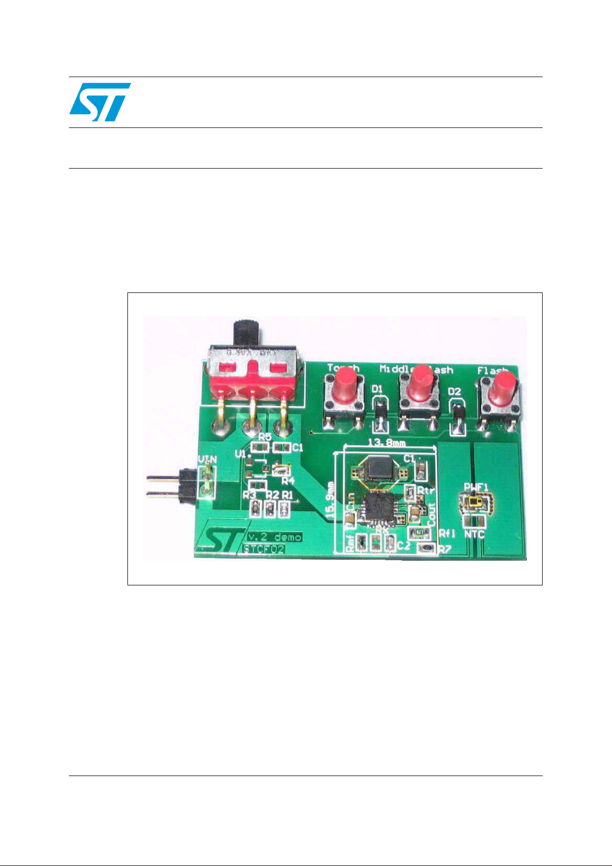
Photo of reference design board
February 2007 Rev 4 1/
www.st.com
Page 2

Contents AN2304
Contents
1 Schematic description . . . . . . . . . . . . . . . . . . . . . . . . . . . . . . . . . . . . . . . 3
1.1 Application schematic . . . . . . . . . . . . . . . . . . . . . . . . . . . . . . . . . . . . . . . . . 3
2 Selection of external components . . . . . . . . . . . . . . . . . . . . . . . . . . . . . . 5
2.1 Input and output capacitor selection . . . . . . . . . . . . . . . . . . . . . . . . . . . . . . 5
2.2 Inductor selection . . . . . . . . . . . . . . . . . . . . . . . . . . . . . . . . . . . . . . . . . . . 5
2.3 LED selection . . . . . . . . . . . . . . . . . . . . . . . . . . . . . . . . . . . . . . . . . . . . . . . 6
2.4 RFLASH selection . . . . . . . . . . . . . . . . . . . . . . . . . . . . . . . . . . . . . . . . . . . 6
2.5 RTORCH selection . . . . . . . . . . . . . . . . . . . . . . . . . . . . . . . . . . . . . . . . . . . 6
2.6 RMF selection . . . . . . . . . . . . . . . . . . . . . . . . . . . . . . . . . . . . . . . . . . . . . . 7
2.7 CCOMP selection . . . . . . . . . . . . . . . . . . . . . . . . . . . . . . . . . . . . . . . . . . . . 7
2.8 NTC and Rx resistor selection . . . . . . . . . . . . . . . . . . . . . . . . . . . . . . . . . . 7
3 PCB design . . . . . . . . . . . . . . . . . . . . . . . . . . . . . . . . . . . . . . . . . . . . . . . . 8
3.1 PCB design rules . . . . . . . . . . . . . . . . . . . . . . . . . . . . . . . . . . . . . . . . . . . . 8
4 Safety shutdown in flash mode . . . . . . . . . . . . . . . . . . . . . . . . . . . . . . . . 9
5 Revision history . . . . . . . . . . . . . . . . . . . . . . . . . . . . . . . . . . . . . . . . . . . 11
2/
Page 3
AN2304 Schematic description
1 Schematic description
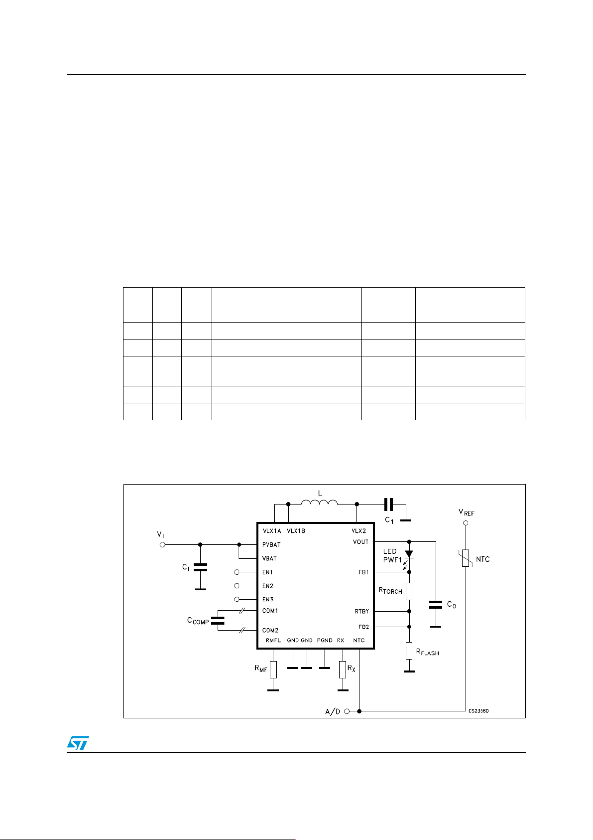
The Flash LED driver is based on STCF02 device with all necessary external components.
High operational frequency (1.8MHz) small size e xte rnal component usage, re sulting a v e ry
compact design of the Flash LED device. The device can operate in five modes:
● Shutdown mode
● Shutdown mode with activated NTC LED temperature sensing
● Torch mode
● Middle flash mode
● Flash mode
These modes can be selected by a combination of logic signals connected to enable pins.
Table 1. Truth table selection mode
EN1 EN2 EN3 ILED
00x 0 0 Shutdown
101 0 0 Shutdown+NTC
0
1
1
1
100 I
110 I
x
1
I
TORCH
MFLASH
= 160mV/(R
= f(I
FLASH
1.1 Application schematic
Figure 1. Typical application schematic
TORCH+RFLASH
, R
FLASH
= 160mV/R
MFLASH
FLASH
ILED_MAX
(mA)
) 250 Torch+NTC
) 500 Medium Flash+NTC
600 Flash+NTC
MODE
3/
Page 4
Schematic description AN2304
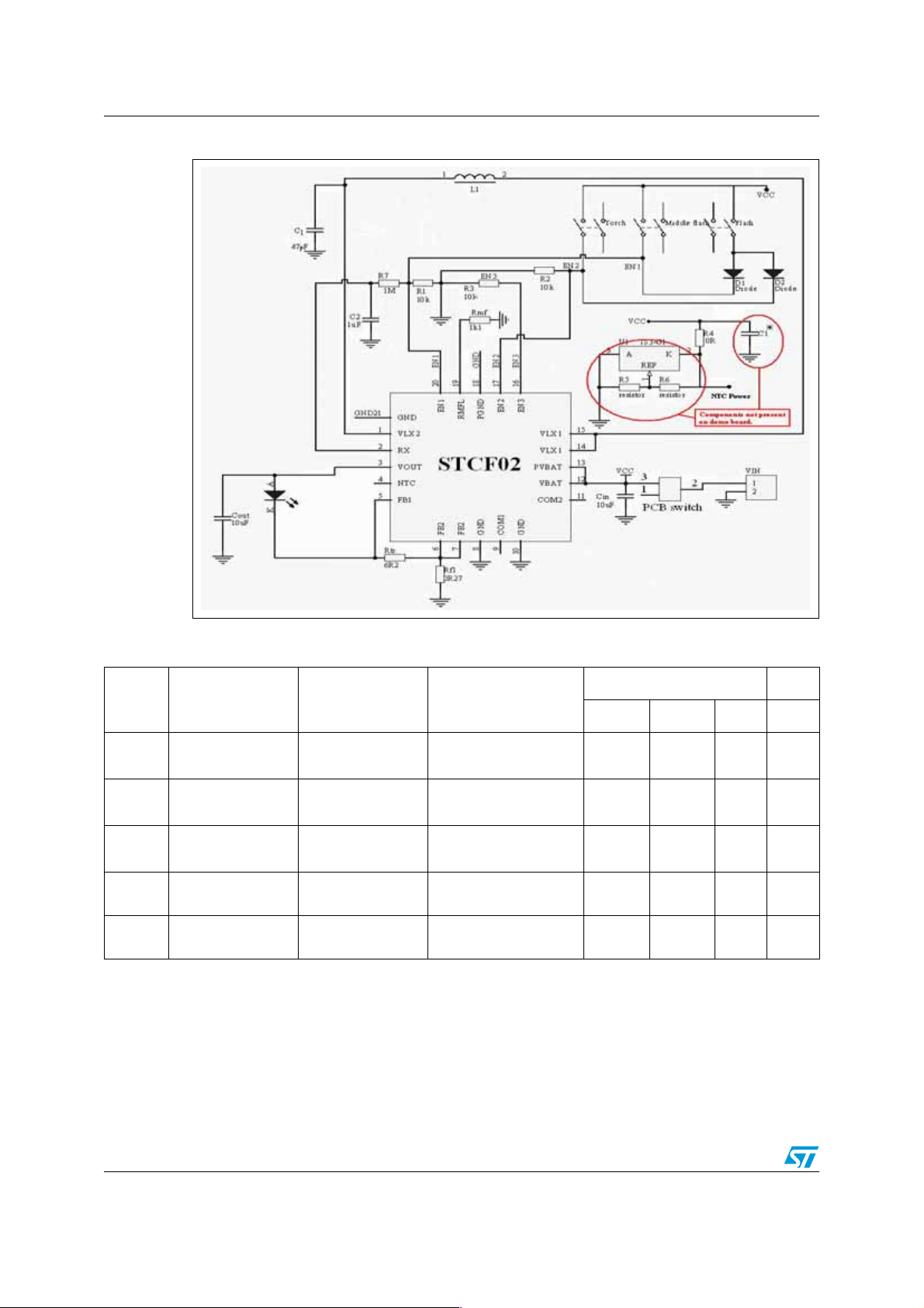
Figure 2. STCF02 Demo board electric schematic
Table 2. STCF02 Demo board BOM List
Symbol Parameter Type
R
FLASH
R
TORCH
R
MF
C
IN
C
OUT
Sensing flash
current resistor
Sensing torch
current resistor
Setting Resistor for
middle flash mode
Input filtering
capacitor
Output capacitor
Thick film type
(0805)
Thick film type
(0603)
Thick film type
(0402)
Ceramic type
(0603) 6.3 V
Ceramic type
(0603) 6.3 V
Supplier & part
number
ROHM
MCR10EZHFLOR27
ROHM
MCR03EZPJ6R20
ROHM
MCR01MZSF1K10
TDK
C1608X5ROJ106MT
TDK
C1608X5ROJ106MT
4
Typ. value Unit
Min Typ Max
0.27 Ohm
6.2 Ohm
1100 Ohm
10 2x10 µF
10 µF
4/
Page 5

AN2304 Selection of external components
Table 2. STCF02 Demo board BOM List (continued)
Symbol Parameter Type
Low profile inductor
L
R1 Anti bump resistor
R2 Anti bump resistor
R3 Anti bump resistor
R4 Resistor
R7
C1 Filtering Capacitor Ceramic (0603) TDK C1608C0J1H470J 47 pF
C2
D1 Schottky diode STPS1L40M
D2 Schottky diode STPS1L40M
4.5(L) x 4.7 (W) x
1.4 (L)
Safety shutdown
resistor
Safety shutdown
capacitor
shielded
DCR 0.12 Ohm
Isat 1.7 A
Thick film type
(0402)
Thick film type
(0402)
Thick film type
(0402)
Thick film type
(0402)
Thick film type
(0402)
Ceramic type
(0603) 6.3 V
Supplier & part
number
TDK VFL5014A-4R7
ROHM
MCR03EZPJ10KR00
ROHM
MCR03EZPJ10KR00
ROHM
MCR03EZPJ10KR00
ROHM
MCR03EZPJ1R00
ROHM
MCR03EZPJ1MR00
TDK
C1608X5ROJ105MT
Typ. value Unit
Min Typ Max
4.7 µF
10 KOhm
10 KOhm
10 KOhm
0Ohm
1MOhm
1µF
LED Luxeon LED PWF1 LXCL-PW1
2 Selection of external components
2.1 Input and output capacitor selection
For input and output capacitors it is recommend ed to use a cer amic capacitor with lo w ESR.
For a good stability of the device supplied by a low input voltage of 2.7 V at maximum
ratings, it is recommended to use 10 uF/6. 3 V as a minim um v a lue of input capacitor and 10
uF/6.3 V as a minimum value of output capacitor.
Note: See recommended components in Table 2.
2.2 Inductor selection
Shielded thick inductor with low DC series resistance of wiring is recommended for this
application. For good efficiency it is recommended to use an inductor with series DC
resistance R
DCL<RD
/10, [Ω, Ω,1] where RD is dynamic resistance of LED.
5/
Page 6

Selection of external components AN2304
For nominal operation, the peak inductor current can be calculated by this formula:
Equation 1
2
I
PEAK
⎛⎞
I
----------- -
⎜⎟
⎝⎠
OUT
n
V
–()V
OUTVin
--------------------------------------------------- -+
2L• F• V
•
•
OUT
IN
V
OUT
--------------
•=
V
2
IN
Where:
–I
–I
Peak inductor current
PEAK
Current sourced at the VOUT pin
OUT
– n Efficiency of the STCF02
–V
–V
Output voltage at the pin Vout
OUT
Input voltage at the pin Vin
IN
– L Inductance value of the inductor
– F Switching frequency
Note: See recommended components in Table 2.
2.3 LED selection
Any LED with forw ard voltage from 2.7 V to 5 V is f easib le for use with device STCF 02. LED
forward voltage must include the voltage spread of this value. It is possible to set the LED
current in the three different operating modes (torch, medium flash, high flash) through three
external sensing resistors.
Note: See recommended components in Table 2.
2.4 R
R
P
FLASH
FLASH
RFLASH=RFLASH*IFLASH
selection
resistor can be selected by equations R
2
, where PRFLASH is the dissipated power on R
recommended to use thick metal film resistor 0603 package size with 1% tolerance.
Maximum flash LED current for STCF02 device is 600mA in battery voltage range from 2.7
V to 5.5 V.
2.5 R
R
TORCH
TORCH
selection
resistor can be selected by equations:
Equation 2
160mV I
R
TORCH
-----------------------------------------------------------------------------=
=160mV/I
FLASH
•()–
TORCHRFLASH
I
TORCH
FLASH
and
FLASH
resistor. It is
Equation 3
P
RTORCHRTORCH
6/
=
I2•
TORCH
Page 7

AN2304 Selection of external components
where P
RTORCH
is the dissipated power on R
metal film resistor with 1% or 5% tolerance. Maxim um torch LED current f or STCF02 device
is 250 mA in voltage range from 2.7 V to 5.5 V.
2.6 RMF selection
With this resistor it is possible to set the LED current value in middle flash mode. The value
of R
resistor is defined by equation:
MF
Equation 4
where I
package size.
2.7 C
This component could optionally be used if the error amplifier bandwidth, which is set to
2kHz default, has to be decreased in case of unstable function of driver, which could cause
the use of different inductor and output capacitor values. It is recommended to use a
ceramic capacitor in 0402 package size.
COMP
is middle flash LED current. It is recommended to use thick film resistor in 0402
MF
selection
I
MF
resistor. It is reco mme nded t o use thick
TORCH
5–
10
⎛⎞
-----------
=
3000
⎝⎠
R
FL
13000 R
--------------------------------- -+
13000 R
•
+
MF
MF
2.8 NTC and Rx resistor selection
The NTC resistor for sensing LED temperature and the Rx resistor create the voltage
divider. Output of this divider is compared to the internal voltage reference 1.192 V. When
the voltage of the voltage divider output is increased over the reference, the logic will switch
off the power circuit.
The maximum current, which could flow through the NTC pin is 1mA. Voltage divider must
be supplied from an external voltage source.
7/
Page 8

PCB design AN2304
3 PCB design
3.1 PCB design rules
STCF02 is a powerful switched device, the PCB must be designed in line with rules for
designing switched supplies. It is recommended to use at least four layers PCB to save the
area on application PCB. The pow er wirings must be as short as possible and wide,
because of large current. Place all external components close to the STCF02. High-energy
switched loops should be as small as possible to reduce EMI. Most of LEDs need cooling,
which could be done by defi ned area of copper on the PCB. Use t he ref erence guide of each
LED to design the heatsink. Place the RFLASH resistor as close as po ssible to pin 8. When
the change of PCB layer is needed, use enough vias. Place the NTC resistor as close as
possible to LED for good temperature sensing. Direct connection of GND and PGND is
needed to achieve correct value of outp ut current. The Led current should not flow through
this track! Sensing of the v oltage on the Rflash resistor has to be done with a wire from pin 7
directly connected to Rflash resistor, no current flows through this track. Pin 6 and pin 7
have to be connected on the pin of Rflash resistor. Expose pad has to be connected to the
PGND with a track as wide as possible.
Figure 3. PCB layout
+
-
Input supply range = 2.7 V to 5.5 V
● Torch mode selection: pushing the Torch button, we will have 25 mA current flowing
through the WLed, no time limit is present. Is possible to reach up to 250 mA of torch
current calculating the R
Equation 5
8/
resistor using this formula:
torch
I
TORCH
16mV
------------------------------------------------- -=
R
+
TORCHRFLASH
Page 9

AN2304 Safety shutdown in flash mode
● Medium Flash mode selection: pushing the Medium Flash button, we will ha ve 150 mA
current flowing through the WLed, safety shutdown is active and after maximum 0.5
sec. the WLed will be turned off. Is possible to reach up to 500 mA of medium Flash
current calculating the Rmflash resistor using this formula:
Equation 6
5–
I
--------------------------------------------------------------------------------- -=
MF
R
FL
● Full Flash mode selection: pushing the Full Flash button, we will have 600 mA current
10
•
13000 R
⎛⎞
3000
----------------------------------
+•
⎝⎠
13000 R
MF
+
MF
flowing through the WLed, safety shutdown is active and after maximum 0.5 sec. the
WLed will be turned off. Is possible to reach up to 600 mA of full Flash current
calculating the Rflash resistor using this f ormula:
Equation 7
I
FLASH
160mV
-------------------- -=
R
FLASH
4 Safety shutdown in flash mode
Alternatively to NTC temperature sensing and protection, it is possible to properly drive all
the STCF02 features with only the EN1 and EN2 pins and include the safety shutdown
mode. This feature has to be active only for Mid Flash and Full Flash operating mode
because in Torch mode there is no risk of burning the LED because of the low current
flowing through it.
The purpose of this specific application is to avoid LED burning if the microcontroller does
not work properly (this means EN1 and/or EN2 are pins stu c k in a hig h logic level). If EN2 is
stuck at high level while EN1 still in low level, the selected mode is Torch, and the safety
shutdown in not needed.
If EN1 is stuck at high level, the STCF02 is in Mid/Full Flash mode and the LED should be
protected from long time operation at high peak current. In this condition, after an RC
defined time, the LED automatically go es off and sta ys off wait ing fo r EN1/EN2 pin resuming
at low level.
After the microcontroller reset, both EN pins will go at low lev el (device enters "All off" mode)
and the capacitor is discharged. At this point, the STCF02 is ready to resume the normal
operating mode.
In typical operating conditions safety shutdown time is about 500msec. This is possible by
applying an RC filter with R=1 MOhm and C=0.47 uF.
9/
Page 10

Safety shutdown in flash mode AN2304
Figure 4. Safety shutdown RC circuit
Figure 5. Safety shut down graphics
Operation for RC filter R=1M Ohm, C=1.0 uF; VLX1 switching voltage (dark blue), during
flash mode with EN1 voltage in high level (light blue). The RX pin voltage (violet) increases
and the output current (light green) goes down after one second (1.192 V threshold
reached).
10/
Page 11

AN2304 Revision history
5 Revision history
Table 3. Revision history
Date Revision
26-Jan-2006
04-Apr-2006
25-May-2006
06-Feb-2007
Changes
1
2
3
First issue
- Pictures changed
- New values added in table “Bill of Material“
- Pictures changed
- Pictures changed
4
- BOM changed
- Minor text changes
11/
Page 12

AN2304
Please Read Carefully:
Information in this document is provided solely in connection with ST products. STMicroelectronics NV and its subsidiaries (“ST”) reserve the
right to make changes, corrections, modifications or improvements, to this document, and the products and services described herein at any
time, without notice.
All ST products are sold pursuant to ST’s terms and conditions of sale.
Purchasers are solely res ponsibl e fo r the c hoic e, se lecti on an d use o f the S T prod ucts and s ervi ces d escr ibed he rein , and ST as sumes no
liability whatsoever relati ng to the choice, selection or use of the ST products and services described herein.
No license, express or implied, by estoppel or otherwise, to any intellectual property rights is granted under this document. If any part of this
document refers to any third pa rty p ro duc ts or se rv ices it sh all n ot be deem ed a lice ns e gr ant by ST fo r t he use of su ch thi r d party products
or services, or any intellectua l property c ontained the rein or consi dered as a warr anty coverin g the use in any manner whats oever of suc h
third party products or servi ces or any intellectual property contained therein.
UNLESS OTHERWISE SET FORTH IN ST’S TERMS AND CONDITIONS OF SALE ST DISCLAIMS ANY EXPRESS OR IMPLIED
WARRANTY WITH RESPECT TO THE USE AND/OR SALE OF ST PRODUCTS INCLUDING WITHOUT LIMITATION IMPLIED
WARRANTIES OF MERCHANTABILITY, FITNESS FOR A PARTICUL AR PURPOS E (AND THEIR EQUIVALE NTS UNDER THE LAWS
OF ANY JURISDICTION), OR INFRINGEMENT OF ANY PATENT, COPYRIGHT OR OTHER INTELLECTUAL PROPERTY RIGHT.
UNLESS EXPRESSLY APPROVED IN WRITING BY AN AUTHORIZED ST REPRESENTATIVE, ST PRODUCTS ARE NOT
RECOMMENDED, AUTHORIZED OR WARRANTED FOR USE IN MILITARY, AIR CRAFT, SPACE, LIFE SAVING, OR LIFE SUSTAINING
APPLICATIONS, NOR IN PRODUCTS OR SYSTEMS WHERE FAILURE OR MALFUNCTION MAY RESULT IN PERSONAL INJ URY,
DEATH, OR SEVERE PROPERTY OR ENVIRONMENTAL DAMAGE. ST PRODUCTS WHICH ARE NOT SPECIFIED AS "AUTOMOTIVE
GRADE" MAY ONLY BE USED IN AUTOMOTIVE APPLICATIONS AT USER’S OWN RISK.
Resale of ST products with provisions different from the statements and/or technical features set forth in this document shall immediately void
any warranty granted by ST fo r the ST pro duct or serv ice describe d herein and shall not cr eate or exten d in any manne r whatsoever , any
liability of ST.
ST and the ST logo are trademarks or registered trademarks of ST in various countries.
Information in this document su persedes and replaces all informatio n previously supplied.
The ST logo is a registered trademark of STMicroelectronics. All other names are the property of their respective owners.
© 2007 STMicroelectronics - All rights reserved
STMicroelectronics group of compan ie s
Australia - Belgium - Brazil - Canada - China - Czech Republic - Finland - France - Germany - Hong Kong - India - Israel - Italy - Japan -
Malaysia - Malta - Morocco - Singapore - Spain - Sweden - Switzerland - United Kingdom - United States of America
www.st.com
12/
 Loading...