

Page 1
AN2269
Application Note
Using the ST8024 Smartcard Interface
Introduction
This application note provides information and suggestions for the optimal use and
performance of the ST8024 Smartcard Interface, including PCB layout, external component
placement, and connections (see
The ST8024 is a smart card interface designed to minimize microprocessor hardware and
software complexity in all applications that require a smar t card (e.g., Set Top Box,
Electronic Payment, Pay TV, and Identification cards). It was devel oped in accordance with
New Digital Systems (NDS) conditional access requirements, and implements all of the
blocks and procedures for card activation/deactivation and checking (see
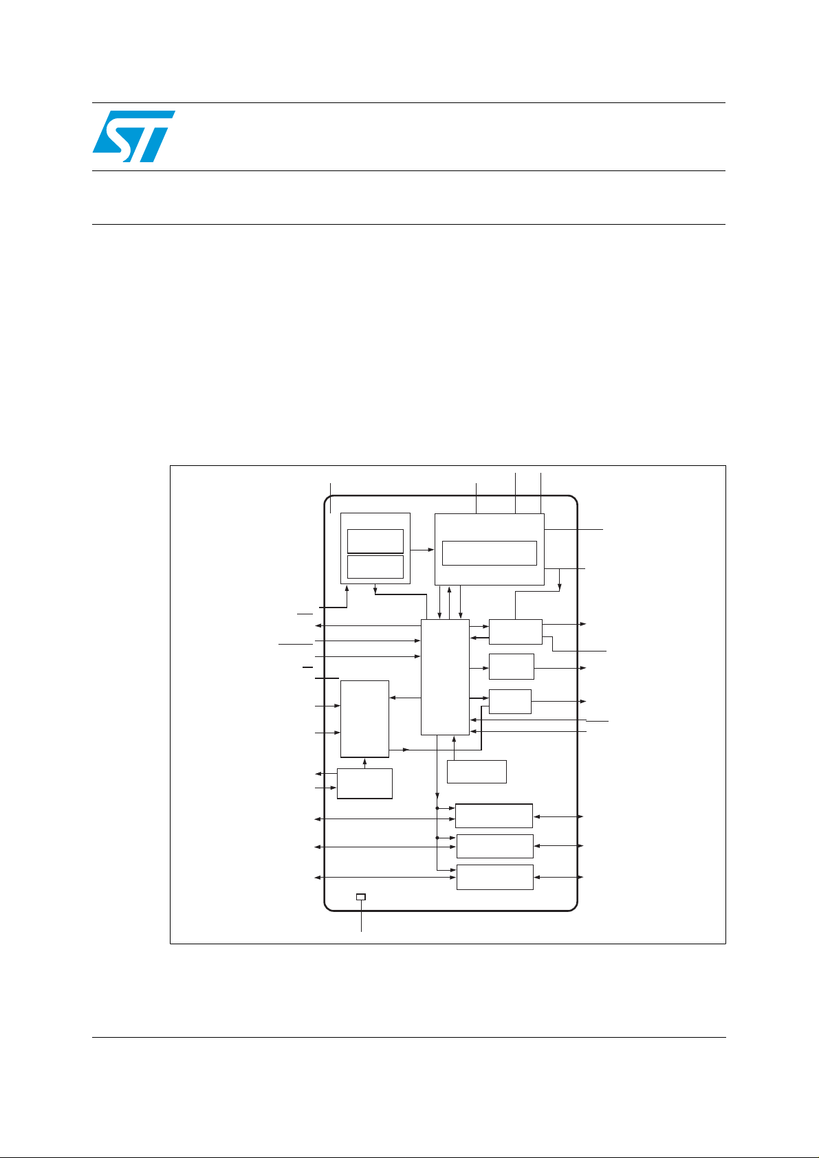
Figure 1. ST8024 Internal Block Diagram
ST8024 Application Hardware Guidelines on page 16
Figure 1
).
).
PORADJ
OFF
RSTIN
CMDV
CC
5V/3V
CLKDIV1
CLKDIV2
XTAL1
XTAL2
AUX1UC
AUX2UC
I/O UC
V
DD
21 6 7
Supply
Internal
Reference
Voltage
Supervisor
Clock
Circuitry
Oscillator
Alarm
En4
CLK
18
23
20
19
3
1
2
24
25
27
28
26
V
REF
Sequencer
En3
V
DDP
ST8024
Oscillator 2.5MHz
En1
Thermal
Protection
S1
Step-up
Converter
Internal
CLKUP
En2
Generator
PV
CC
En5
RST
Buffer
En4
Clock
Buffer
I/O T ransceiver
I/O T ransceiver
I/O T ransceiver
S2
5
P
4
GND
V
8
UP
V
17
V
CC
CC
CGND
14
RST
16
CLK
15
PRES
10
PRES
9
AUX1
13
AUX2
12
I/O
11
22
GND
AI11884
February 2006 Rev 1 1/25
www.st.com
Page 2

Table of Contents AN2269 - Application Note
Table of Contents
1 Activation/Deactivation Sequence . . . . . . . . . . . . . . . . . . . . . . . . . . . . . . 4
2 Card Clock . . . . . . . . . . . . . . . . . . . . . . . . . . . . . . . . . . . . . . . . . . . . . . . . . 6
3 Emergency Deactivation/Fault Detection . . . . . . . . . . . . . . . . . . . . . . . . 7
3.1 PORAD J VDD Undervoltage without External Resistor Bridge . . . . . . . . . 7
3.2 PORAD J V
3.3 Fault On Card Removal . . . . . . . . . . . . . . . . . . . . . . . . . . . . . . . . . . . . . . 12
3.4 V
3.5 V
3.6 Over-Temperature Fault Protection . . . . . . . . . . . . . . . . . . . . . . . . . . . . . 15
Short Circuit Fault Protection . . . . . . . . . . . . . . . . . . . . . . . . . . . . . . 13
CC
Drop . . . . . . . . . . . . . . . . . . . . . . . . . . . . . . . . . . . . . . . . . . . . . . . . 15
DDP
Undervoltage with External Divider . . . . . . . . . . . . . . . . . . . 9
DD
4 ST8024 Application Hardware Guidelines . . . . . . . . . . . . . . . . . . . . . . 16
4.1 Power Supply Optimization . . . . . . . . . . . . . . . . . . . . . . . . . . . . . . . . . . . 18
4.2 Clock Section Optimization . . . . . . . . . . . . . . . . . . . . . . . . . . . . . . . . . . . 20
4.3 Smart Card Connections . . . . . . . . . . . . . . . . . . . . . . . . . . . . . . . . . . . . . 21
5 Revision History . . . . . . . . . . . . . . . . . . . . . . . . . . . . . . . . . . . . . . . . . . . 24
2/25
Page 3

AN2269 - Application Note List of Figures
List of Figures
Figure 1. ST8024 Internal Block Diagram . . . . . . . . . . . . . . . . . . . . . . . . . . . . . . . . . . . . . . . . . . . . . . 1
Figure 2. ST8024 Activation Sequence . . . . . . . . . . . . . . . . . . . . . . . . . . . . . . . . . . . . . . . . . . . . . . . . 4
Figure 3. Deactivation Sequence. . . . . . . . . . . . . . . . . . . . . . . . . . . . . . . . . . . . . . . . . . . . . . . . . . . . . 5
Figure 4. CLKDIV Change Clock Duty Cycle. . . . . . . . . . . . . . . . . . . . . . . . . . . . . . . . . . . . . . . . . . . . 6
Figure 5. ST8024 Automatic Deactivation Sequence . . . . . . . . . . . . . . . . . . . . . . . . . . . . . . . . . . . . . 8
Figure 6. External Resistor Bridge Applied to PORADJ . . . . . . . . . . . . . . . . . . . . . . . . . . . . . . . . . . . 9
Figure 7. V
Figure 8. V
TH(ext) rise
TH(ext) fall
Figure 9. Card Extraction. . . . . . . . . . . . . . . . . . . . . . . . . . . . . . . . . . . . . . . . . . . . . . . . . . . . . . . . . . 12
Figure 10. ST8024 Activation Sequence (after t
Figure 11. ST8024 Current Supply Sequence. . . . . . . . . . . . . . . . . . . . . . . . . . . . . . . . . . . . . . . . . . . 13
Figure 12. I
Short Circuit Protection . . . . . . . . . . . . . . . . . . . . . . . . . . . . . . . . . . . . . . . . . . . . . . . . . 14
SC
Figure 13. Deactivation Caused By V
Figure 14. ST8024 Application PCB Top Layer. . . . . . . . . . . . . . . . . . . . . . . . . . . . . . . . . . . . . . . . . . 16
Figure 15. ST8024 Application PCB Bottom Layer . . . . . . . . . . . . . . . . . . . . . . . . . . . . . . . . . . . . . . . 17
Figure 16. Step-up Converter Block Diagram . . . . . . . . . . . . . . . . . . . . . . . . . . . . . . . . . . . . . . . . . . . 18
Figure 17. ST8024 Application PCB Storage and Pumping Capacitors . . . . . . . . . . . . . . . . . . . . . . . 19
Figure 18. ST8024 Application PCB Crystal (XTAL) Connection. . . . . . . . . . . . . . . . . . . . . . . . . . . . . 20
Figure 19. ST8024 Application PCB Smart Card Connections . . . . . . . . . . . . . . . . . . . . . . . . . . . . . . 21
Figure 20. Ripple on V
Figure 21. ST8024 Application PCB Schematic . . . . . . . . . . . . . . . . . . . . . . . . . . . . . . . . . . . . . . . . . 23
(External Rising Threshold Voltage on VDD) . . . . . . . . . . . . . . . . . . . . . . . . . . 10
(External Falling Thres hold on VDD) . . . . . . . . . . . . . . . . . . . . . . . . . . . . . . . . . 11
debounce
Drop. . . . . . . . . . . . . . . . . . . . . . . . . . . . . . . . . . . . . . . . . . 15
DDP
Output Voltage . . . . . . . . . . . . . . . . . . . . . . . . . . . . . . . . . . . . . . . . . . . . . . 22
CC
) . . . . . . . . . . . . . . . . . . . . . . . . . . . . . . . . . . 12
3/25
Page 4
Activation/Deactivation Sequence AN2269 - Application Note
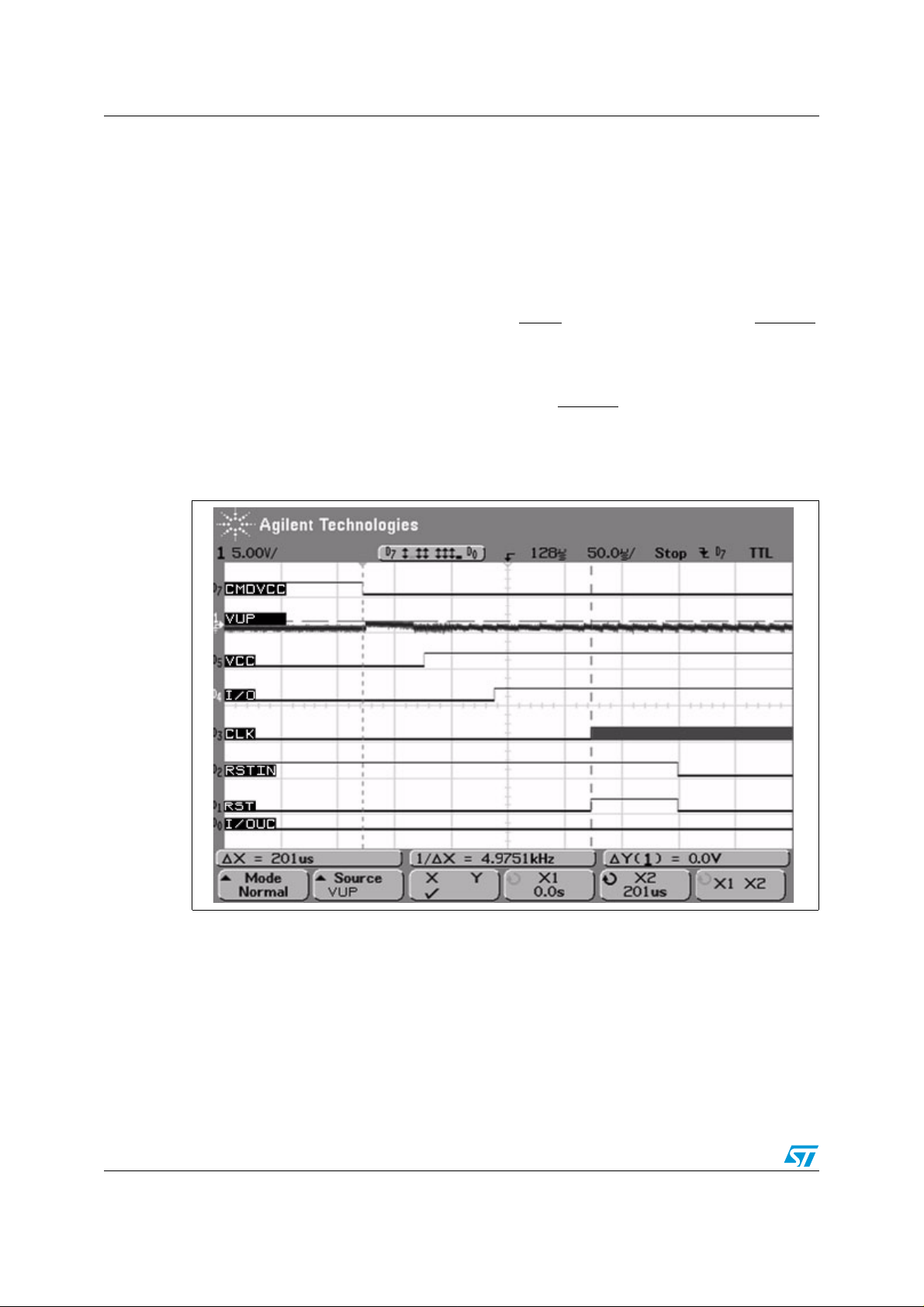
1 Activation/Deactivation Sequence
The core of the ST8024 is the sequencer (shown in
coordinate the Enable signals for the activation and deactivation sequence as well as check
for possible fault conditions. This because the smart card is basically a microcontroller and
needs to be activated/deactivated by a correct sequence as required by the ISO/IEC7816
standard. The ST8024 activation and deactivation sequences are shown in
Figure 3 on page 5
Figure 2
goes low. The activation sequence starts and the first block to be enabled is the step-up
converter (V
allows the card software to start.
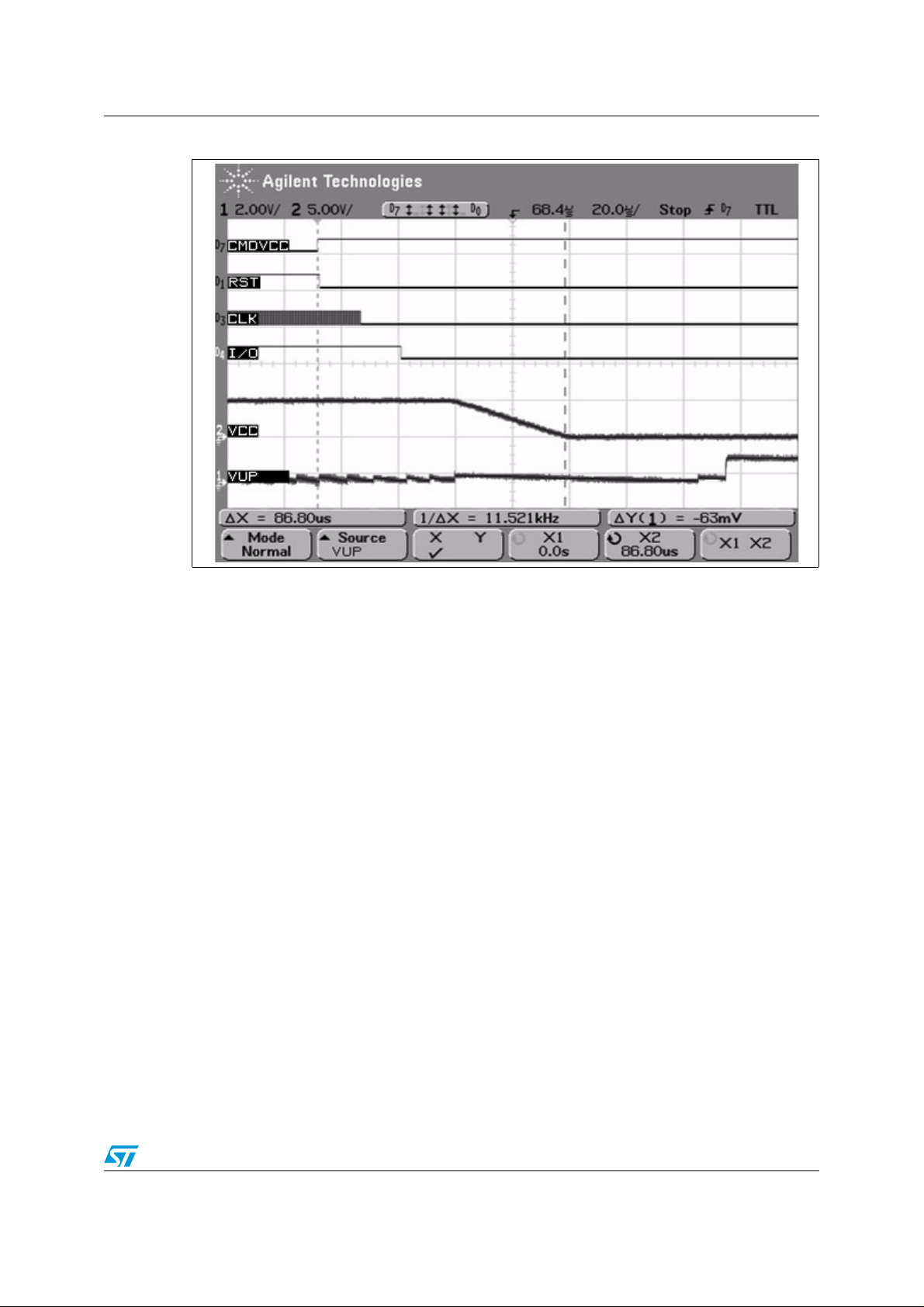
Figure 3
executes an automatic deactivation sequence, finishing in the inactive state after t
(deactivation time).
Figure 2. ST8024 Activation Sequence
shows that the PRES condition is true (PRES = low or PRES = high), and CM DVcc
shows the deactivation sequence (when the CMDVcc goes high). The circuit
, respectively. Please refer to the ST8024 datasheet for details.
), linked to En1 (see
UP
Figure 1
), while the last enabled signal is the RST that
Figure 1 on page 1
) that must
Figure 2
de
and
4/25
Page 5
AN2269 - Application Note Activation/Deactivation Sequence
Figure 3. Deactivation Sequence
5/25
Page 6
Card Clock AN2269 - Application Note
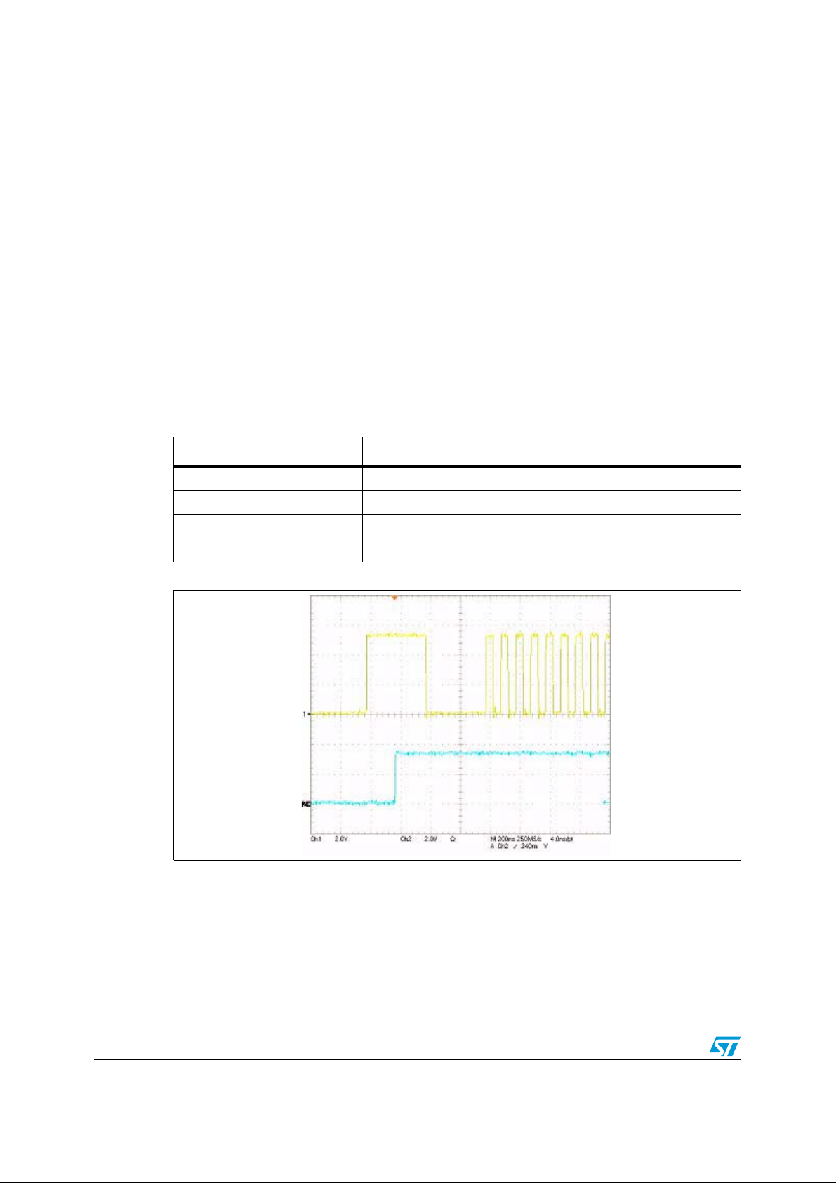
2 Card Clock
The card clock signal (CLK) is present on the CLK pin when the ST8024 is activated; it is
linked with the internal En4 signal (see
according to the settings in
Table 1
According to the ISO/IEC7816 specifications, the CLK duty cycle must be guaranteed
between 45% and 55%, even when the status of CLOCKDIV1 or CLOCKDIV2 changes.
Figure 4
shows how the ST8024 ensures duty cycle accuracy by waiting for completion of a
whole clock cycle before changing the frequency (CLKDIV1 change, rising edge of CH2).
The output Duty Cycle is 50%±5%, even if the Clock Division changes.
The card clock signal (CLK) can be obtained by connecting a crystal (“XTAL”) between the
XTAL1 and XTAL2 pins, or by an external signal applied to the XTAL1 pin. In this case the
XTAL2 pin must be left floating. The external signal voltage level must be limited between
GND and V
Table 1. CLK Division Factor
voltage.
DD
Figure 1 on page 1
.
) and its frequency is obtained
CLKDIV1 CLKDIV2 f
0 0 1/8 f
011/4 f
1 1 1/2 f
10f
Figure 4. CLKDIV Change Clock Duty Cycle
clk
Xtal
XtalL
Xtal
Xtal
Legend:
1. CH1 = Output CLK Waveform
2. CH2 = CLKDIV1 Pin
3. Conditions: V
4. Mode: ACTIVE
5. f
= 10MHz; CLKDIV2 = 0V
XTAL
= 3.3V; V
DD
6/25
= 5V; 5/3V = H
DDP
Page 7

AN2269 - Application Note Emergency Deactivation/Fault Detection
3 Emergency Deactivation/Fault Detection
ST8024 is equipped with a fault detection circuitry which monitors the following conditions
(see
Figure 1 on page 1
● V
● Fault on card removal,
● V
● V
● Over-Temperature protection.
undervoltage,
DD
Short circuit protection,
CC
drop, and
DDP
3.1 PORADJ VDD Underv oltage without External Resistor Br idge
The ST8024 logic circuitry is supplied by VDD. In order to avoid voltage spikes that could
cause damage, or malfunction of the device and/or card, a voltage supervisor block is
embedded (see
(Falling Threshold Voltage on V
deactivation sequence and V
As V
goes higher than V
DD
100mV, typ), after a certain amount of time (t
reset pulse width, 8ms typ, see
sequence starts and V
to GND to avoid noise capture is recommended.
Figure 1
):
). This block monitors VDD and when it gets lower than V
, 2.45V, typ), the supervisor immediately starts the
DD
goes low.
CC
+ V
TH2
Figure 5 on page 8
goes high. The PORADJ pin can be left floating, but connecting it
CC
HYS2
, (V
is the Hysteresis of threshold voltage,
HYS2
+ t
w
debounce
, where tw is the internal power-on
), CMDVcc goes low. The activation
TH2
Note: See
Fault On Card Removal on page 12
for t
debounce
feature details.
7/25
Page 8
Emergency Deactivation/Fault Detection AN2269 - Application Note
Figure 5. ST8024 Automatic Deactivation Sequence
Note: Deactivation: V
Activation: As V
Legend:
1. CH1 = CMDVcc
2. CH2 = V
3. CH3 = OFF
4. CH4 = V
5. Conditions: VDD = 3.3V; V
6. Mode: ACTIVE
7. f
CC
DD
= 10MHz; CLKDIV2 = 0V
XTAL
≈ 2.393V.
TH2
≥ V
DD
+ V
TH2
= 5V; 5/3V = H
DDP
(≈ 2.498V) AND CMDVcc goes low, VCC goes high.
HYS2
8/25
Page 9

AN2269 - Application Note Emergency Deactivation/Fault Detection
3.2 PORADJ VDD Undervoltage with External Divider
In this case, a resistor bridge is applied to the PORADJ pin (see
V
TH(ext) fall
Voltage on V
are the External Rising Threshold Voltage and the External Falling Threshold
, respectively. They are the voltages on pin PORADJ that switch the device
DD
Figure 6
). V
TH(ext) rise
and
ON and OFF. By knowing these values and using the formula:
V
PORADJ
R2R1R2+⁄()VDD×=
Where:
it is possible to set R
device ON and OFF (R
In particul a r, R
1
and R2 in order to get suitable values for VDD in order to turn the
1
= 100kΩ typ).
1+R2
and R2 have to be set so that, when VDD is getting low, before turning the
microcontroller off, the smart card has to be switched off properly as well. The same goes
for microcontroller start-up. The smart card has to be turned on after the microcontroller.
Figure 7
and
Figure 8 on page 11
show the V
TH(ext) rise
and V
TH(ext) fall
on the PORADJ pin
(0.21V and 1.15V, respectively).
As long as V
for t
+ t
w
debounce
gets the proper start-up value (so that V
DD
by the CMDVcc
16ms (while OFF
(tw ≈ 16ms, in this case). During this time, the device can not be turned on
TH(ext) rise
. To turn th e device on, CMDVcc must go low at least by the end of about
is high).
= 1.196V), OFF goes low
Figure 6. External Resistor Bridge Applied to PORADJ
V
DD
GND
R1
To PORADJ
R2
AI11885
9/25
Page 10

Emergency Deactivation/Fault Detection AN2269 - Application Note
Figure 7. V
Legend:
1. CH1 = CMDVcc
2. CH2 = V
3. CH3 = OFF
4. CH4 = V
CC
TH(ext) rise
TH(ext) rise
(External Rising Threshold Voltage on VDD)
10/25
Page 11

AN2269 - Application Note Emergency Deactivation/Fault Detection
Figure 8. V
Note: As V
Legend:
1. CH1 = CMDVcc
2. CH2 = V
3. CH3 = OFF
4. CH4 = V
TH(ext) rise
CC
TH(ext) fall
TH(ext) fall
(External Falling Threshold on VDD)
= 1.155V, the device starts switching OFF and VCC goes low.
11/25
Page 12

Emergency Deactivation/Fault Detection AN2269 - Application Note
3.3 Fault On Card Removal
If the smart card is pulled out from its socket (PRES goes high or PRES goes low), the
deactivation sequence starts. The OFF
Figure 9
). In order to avoid bouncing on the PRES (or PRES) signal at card insertion or
extraction, as the card is inserted again, OFF
If CM DVcc
and CMDVcc
Figure 10 on page 12
goes low before this time, after card insertion, the device does not turn itself on
must wait for t
debounce
shows the start of the activation sequence after t
Figure 9. Card Extraction
pin goes low and the device switches off (see
goes high just after a period t
debounce
(≈ 8ms).
before going low enough to switch the device on.
debounce
is elapsed.
Figure 10. ST8024 Activation Sequence (after t
12/25
debounce
)
Page 13

AN2269 - Application Note Emergency Deactivation/Fault Detection
3.4 VCC Short Circuit Fault Protection
The ST8024 is able to supply the card with current pulses of about 140mA f or no longer than
5.5µs, typical (see
Short circuit protection is an important interface feature that warns the sequencer block if
the output current becomes higher than the short circuit current li mit (≈120mA) for too much
time. This characteristic allows the de vice to supply the card with current pulses higher than
the maximum allowed, if their lengths are not too long. If the current pulses last for more
than 5.5µs, the deactivation sequence starts to protect the card. The OFF
as to warn the microcontroller about the overcurrent fault. The sequence in
page 14
shows how the current pulse becomes long enough to make the short circuit
protection happen.
Figure 11. ST8024 Current Supply Sequence
Figure 11
and
Figure 12 on page 14
).
pin goes low so
Figure 12 on
Legend:
1. CH1 = CMDVcc
2. CH2 = ISC Pulse
3. CH3 = V
4. CH4 = OFF
CC
13/25
Page 14

Emergency Deactivation/Fault Detection AN2269 - Application Note
Figure 12. ISC Short Ci rcuit Protection
14/25
Page 15

AN2269 - Application Note Emergency Deactivation/Fault Detection
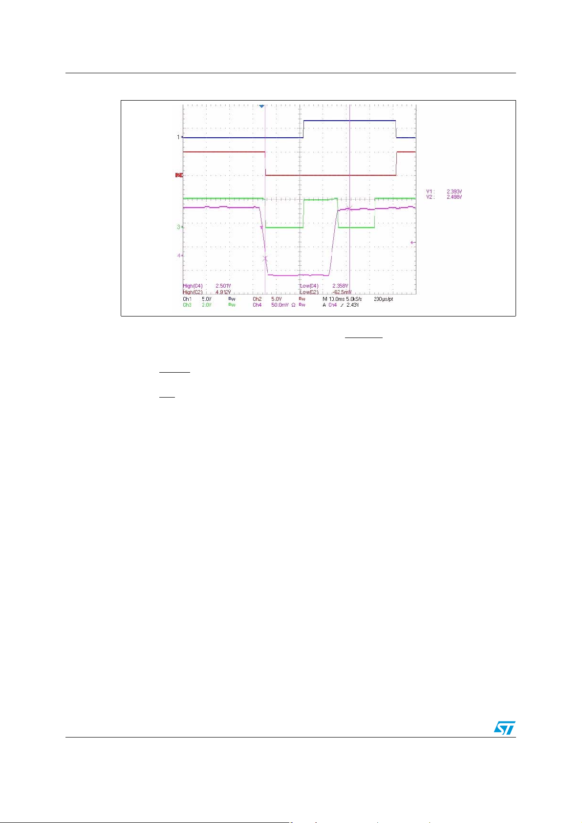
3.5 V
The voltage supervisor also controls the V
(≈2.578V, in this case, see
Figure 13. Deactivation Caused By V
Legend:
1. CH1 = V
2. CH2 = CMDVcc
3. CH3 = V
4. CH4 = OFF
DDP
Drop
DDP
CC
Figure 13
Drop. As it reaches the minimum value
DDP
, the OFF pin goes low and the VCC drops.
Drop
DDP
3.6 Over-Temperature Fault Protection
Over-Temperature protection is another impor ta nt interface feature that warns the
sequencer block of fault events. If the temperature is higher than the shutdown temperature
(150°C, typ), the deactivation sequence starts to protect the card. The OFF
as to warn the microcontroller about the over-temperature fault.
pin goes low so
15/25
Page 16

ST8024 Application Hardware Guidelines AN2269 - Application Note
4 ST8024 Application Hardware Guidelines
This section contains some optimization guidelines concerning PCB la yout as well as
external component placement and connections. The referenced application board in
Figure 14
application NDS requirements.
The PCB layout provides completely separate supply and GND copper planes, which allow
each plan to act as a shield for each group of noise-sensitive device pins. The PGND, and
CGND and GND planes share a common point on bottom layer of the PCB (see top,
Figure 15 on page 17
Figure 14. ST8024 Application PCB Top Layer
and
Figure 15 on page 17
).
has two layers, and uses these guidelines to meet
16/25
Page 17

AN2269 - Application Note ST8024 Application Hardware Gu idelines
Figure 15. ST8024 Application PCB Bottom Layer
17/25
Page 18

ST8024 Application Hardware Guidelines AN2269 - Application Note
4.1 Power Supply Optimization
The ST8024 can drive both 3V and 5V cards by the supply voltage selector pin 5/3V (pin 3)
as shown in
and if the 5/3V is connected to V
A step-up converter supplied by V
input voltage V
● 5/3V=H and V
● 5/3V=H and V
● 5/3V=L and V
● 5/3V=L and V
The S1 and S2 pins are used for duplicating the supply voltage V
pumping capacitor (C4). The charge pump output pin (V
storage capacitor (C5) to stabilize the voltage.
Figure 16. Step-up Converter Block Diagram
Figure 1 on page 1
or follows it, depending on the 5/3V and V
DDP
> 5.8 V; voltage follower
DDP
< 5.7 V; voltage doubler
DDP
> 4.1 V; voltage follower
DDP
< 4.0 V; voltage doubler
DDP
. If the 5/3V pi n is connected to GND, the VCC voltage is 3V,
, the VCC voltage is 5V.
DD
is used for the VCC voltage generation. It doubles the
DDP
values:
DDP
by using the 100nF
DDP
) has to be connected to a 100nF
UP
100nF
100nF
S1 S2
65
ON/OFF
Step-up
Mode
Selector
ST8024
EN2
PV
CC
7
OUTPUT
L
V
CC
Regulator
1
7
PGND
V
UP
100nF
V
CC
AI11894
18/25
Page 19

AN2269 - Application Note ST8024 Application Hardware Gu idelines
A small amount of noise is introduced into the design because of the switching circuitry. In
order to reduce it and improve the efficiency of the step-up converter, the capacitors must be
connected as closely as possible to the pins (see
Figure 17
). An Equiva lent Series
Resistance (ESR) of lower than 100mΩ at 100kHz is recommended.
The evaluation board is equipped with MURATA GRM31M 7U1H104JA01B capacitors.
However, other capacitors with an ESR of up to 100mΩ at 100kHz are good enough to work
within the specifications. They just may be more sensitive to the la yout optimization process.
Figure 17. ST8024 Application PCB Storage and Pumping Capacitors
19/25
Page 20

ST8024 Application Hardware Guidelines AN2269 - Application Note
4.2 Clock Section Optimization
Recommendations for the PCB design clock area include:
● The XTAL should be connected as closely as possible to the XTAL pins to reduce signal
reflections, especially for high frequency applications (see
● Two compensation capacitors (C9 and C10), each of 15pF (typ) are suggested to
improve the oscillator start-up performances. Even without those additional capacitors
the CLK Duty Cycle is guaranteed between 45% and 55% (according to the NDS
specifications), with frequencies up to 26MHz.
Figure 18. ST8024 Application PCB Crystal (XTAL) Connection
Figure 18
).
20/25
Page 21

AN2269 - Application Note ST8024 Application Hardware Gu idelines
4.3 Smart Card Connections
In typical applications, a 100nF filter capacitor (C3) is connected to the VCC output towards
GND/CGND, near the ST8024 pins. A second 100nF capacitor (C8) is connected between
the card socket pins C1 (V
to reduce noise and avoid coupling effects, the wire length between the ST8024 and card
should be as short as possible.
Another recommendation is to keep the CLK track far away from the other signal tracks to
limit coupling with the transceiver lines. Further decoupling is gained if the clock track is
shielded by a GND/CGND plane or track on the PCB.
Keeping the PGND and GND/CGND planes as large as possible improves power supply
noise rejection. With this in mind, the board design should connect these planes with a large
number of vias between the top and bottom board layers (3-4 vias per cm
) and C5 (CGND), near the card slot (see
CC
Figure 19
2
).
). In order
The V
applied with V
Figure 20 on page 22
applied and the measured ripple is lower than 160mV
spikes are much lower than 350mVPP, even when a pulsed load of up to 80mA is
CC
= 5V, or up to 65mA with VCC = 3V, as specified b y the NDS requirements.
CC
shows a typical VCC output waveform where an 80mA pulsed load
.
PP
Figure 19. ST8024 Application PCB Smart Card Connections
21/25
Page 22

ST8024 Application Hardware Guidelines AN2269 - Application Note
Figure 20. Rippl e on VCC Output Voltage
Legend:
1. VDD = 3.3V
DDP
= 5V
CC
CC
2. V
3. CH2 = 80mA Pulsed Current I
4. CH4 = Ripple on VCC Output Voltage
5. 5V Offset on V
22/25
Page 23

AN2269 - Application Note ST8024 Application Hardware Gu idelines
Figure 21. ST8024 Application PCB Schematic
A
1
of
1
Wednesday, June 22, 2005
ST8024 Evaluation Board
A4
Title
Size Document Number Rev3Date: Sheet
N.C. or N.O. switch is included in the Smartcard connector.
Please select JP17 as specified in the PRES configuration.
2 - 3
1 - 5
J7
100nF
1 - 4
2 - 5
T.P. card K
B
2
1
VCC
100nF
C8
U1
6
5
Pin 2 of JP17 to J8
RST
4
3
CLK
AUX1
K2
K1
AUX2
I/ONCGND
7
SMARTCARD CONNECTOR
8
9
10
J6
U2
XTAL GND Jumper
10pF
10MHz
AUX2UC
CLKDIV1
C
C1
C10
Y1
25
262728
I/OUC
AUX1UC
CLKDIV2
5V/3V
4
321
C4
24
XTAL2
GNDP
5
XTAL1
S2
23
6
100nF
10pF
22
OFF
VDDP
7
100nF
C5
GND
S1
VCC
19
20
15
16
21
17
18
CLK
RST
VCC
VDD
RSTIN
PORADJ
CMDVCC
C3
VUP
9
8
PRES
10
100nF
PRES
11
CGND
AUX1
AUX2
I/O
ST8024
14
13
12
J1 pins J2 pins
D
6
54321
J3
J2
2.7V - 6.5V
VDD
GND
3
2
1
J14
–OFF
3
2
1
J12
VTHSEL
3
2
1
J11
CMDVCC
3
2
1
J10
RSTIN
+
47µF
C6
C9
J8
J7
J6
J5
J4
J3
I/OUC
AUX1UC
AUX2UC
CLKDIV1
CLKDIV2
5/3V
3
2
1
3
2
1
3
2
1
3
2
1
3
2
1
3
2
1
J1
4V ÷ 6.5V
VDDP
VUP
47µF
330nF
C12
2
1
+
C7
JP18
D
C2
100nF
+PRES (SW N.C.)
–PRES (SW N.O.)
PRES conf.
and SW kind
PRES config (JP17)
Please connect the 2 jumpers as follows:
10KΩ
R6
4
5
3
2
1
JP17
J8
GND-PRES
C
PRES
No Switch
B
J5
T.P. card K
1 2 3 4 56
AI11898
A
23/25
Page 24

Revision History AN2269 - Application Note
5 Revision History
Table 2. Document Revision History
Date Revision Changes
10-Feb-2 006 1 Initial re le a s e.
24/25
Page 25

AN2269 - Application Note
y
y
Please Read Carefully:
Information in this document is provided solely in connection with ST products. STMicroelectronics NV and its subsidiaries (“ST”) reserve the
right to make changes, corrections, modifications or improvements, to this document, and the products and services described herein at an
time, with out notice.
All ST products are sold purs uant to ST’s terms and conditions of sale.
Purchase rs are solely r esponsible for the choice, se l ection and us e of the ST prod ucts and serv i ces described herein, and ST assumes no
liability whatsoever relating to the choice, selection or use of the ST products and services described herein.
No license, express or implied, by estoppel or otherwise, to any intellectual property rights is granted under this document. If any part of this
document refers to any third party product s or services it s hall not be deeme d a license grant by ST for the use of such third part y products
or services , or any intel lec tual pro per ty cont aine d ther ein or con sidere d as a warra nty c overi ng th e use i n any mann er w hats oever of such
third party products or servi ces or any intellectual property cont ai ned therein.
UNLESS OTHERWISE SET FORTH IN ST’S TERMS AND CONDITIONS OF SALE ST DISCLAIMS ANY EXPRESS OR IMPLIED
WARRANTY WITH RESPECT TO THE USE AND/OR SALE OF ST PRODUCTS INCLUDING WITHOUT LIMITATION IMPLIED
WARRANTIES OF MERCHANTABILITY, FITNESS FOR A PARTICULAR PURPOSE (AND THEIR EQUIVALENTS UNDER THE LAWS
OF ANY JURISDICTION), OR INFRINGEMENT OF ANY PATENT, COPYRIGHT OR OTHER INTELLECTUAL PROPERTY RIGHT.
UNLESS EXPRESSLY APPRO VED IN W RITING B Y AN AUTHORIZE REPRESE NTATIVE O F ST, ST PRODU CTS ARE N OT DESI GNED,
AUTHOR I Z ED OR WARRANTED FOR USE IN MILITARY , AIR CRAFT , S PACE, LIF E S AVING, OR L IF E SUSTAINI NG APPLIC AT I O NS,
NOR IN PRODUCTS OR SYSTEMS, WHERE FAILURE OR MALFUNCTION MAY RESULT IN PERSONAL INJURY, DEATH, OR
SEVERE PROPERTY OR ENVIRONMENTAL DAMAGE.
Resale of ST products with provisions different from the statements and/or technical features set forth in this document shall immediately void
any warran ty gr anted by ST fo r the ST produc t or se rvice d es cribed he rein and shall not c reat e o r extend in a ny mann er wha tsoe ver, an
liability of ST.
ST and the ST logo are trademarks or registered trademarks of ST in various countries.
Information in this document supersedes and replaces all information previously supplied.
The ST logo is a registered trademark of STMicroelectronics. All other names are the property of their respective owners.
© 2006 STMi croelectronic s - A l l rights reserved
STMicroelectronics grou p of companies
Austra l i a - Be l gi um - Brazil - Cana da - China - Czech Rep ubl i c - Finland - Franc e - Germany - Hong Kong - India - Israel - It aly - Japan -
Malaysi a - M al ta - Morocco - Sin gapore - Spain - Sweden - Switzerlan d - United Kingdom - Uni ted States of America
www.st.com
25/25
 Loading...