

Page 1

AN2252
Application note
Zero-voltage switching and emitter-switched bipolar transistor
in a 3-phase auxiliary power supply
Introduction
The flyback converter is a popular choice in applications where the required power is
normally less than 200W. The main reasons explaining its popularity are its simplicity, low
cost and high efficiency for a small number of active components.
In switching converters power loss is caused by power dissipation within the parasitic
elements of both passive and active components. Power loss in passive components can be
reduced by selecting suitable passive components and carefully designing the transformer.
Power loss in active components can be improved by selecting suitable active components
and making sure that they are used correctly.
Power loss generated by active components can be divided into two categories:
● conduction loss
● switching loss
The aim of the proposed zero-voltage switching control is to reduce switching loss (in this
application, the primary switch turn-on loss). The zero-voltage switching control also greatly
reduces the EMI generated by primary switch turn-on.
Conduction loss is generated with the device fully turned-on, by the voltage drop across the
conducting device. The proposed use of the Emitter-Switched Bipolar Transistor (ESBT) as
the primary switch reduces conduction loss efficiently. Moreover, with its low saturation
voltage and fast switching capability compared to an IGBT or a bipolar junction transistor
(BJT), the ESBT is well suited for this use. These characteristics are essential in
applications where a high breakdown voltage capability is required.
The reference board presented in this Application Note gives a solution of a power supply
for 3-phase applications like inverters for induction motors, welding machines, UPS etc. Very
commonly in this kind of applications, the neutral line is not available or its use is not
allowed, and only phase-to-phase voltage is available. The nominal European phase-tophase voltage is 400VAC. Taking into account a ±20% tolerance, the rectified input bulk
capacitor voltage can reach up to 680VDC. The zero-voltage switching topology requires a
reflected flyback voltage equal to the input bulk capacitor voltage. For this reason it is
necessary to use a switch which will accept at least 1500V and exhibits a low conduction
loss during the ON-time. The high-voltage MOSFET switches rated for this voltage, available
on the market today are rather expensive due to their large die size. The ESBT, thanks to its
low voltage drop, high speed, square reverse bias safe operating area, smaller die size and
lower price is well suited for use as a high-voltage power switch.
November 2006 Rev 2 1/21
www.st.com
Page 2

Contents AN2252
Contents
1 Theory of ESBT and quasi-resonant operation . . . . . . . . . . . . . . . . . . . 4
2 Application circuit description . . . . . . . . . . . . . . . . . . . . . . . . . . . . . . . . . 7
2.1 Operating conditions . . . . . . . . . . . . . . . . . . . . . . . . . . . . . . . . . . . . . . . . . 7
2.2 Circuit operation . . . . . . . . . . . . . . . . . . . . . . . . . . . . . . . . . . . . . . . . . . . . . 7
2.2.1 Bill of materials . . . . . . . . . . . . . . . . . . . . . . . . . . . . . . . . . . . . . . . . . . . . 9
2.2.2 Transformer design . . . . . . . . . . . . . . . . . . . . . . . . . . . . . . . . . . . . . . . . 11
2.3 PCB Layout . . . . . . . . . . . . . . . . . . . . . . . . . . . . . . . . . . . . . . . . . . . . . . . 13
2.3.1 Evaluation and measurements . . . . . . . . . . . . . . . . . . . . . . . . . . . . . . . 14
3 Conclusion . . . . . . . . . . . . . . . . . . . . . . . . . . . . . . . . . . . . . . . . . . . . . . . . 20
4 References . . . . . . . . . . . . . . . . . . . . . . . . . . . . . . . . . . . . . . . . . . . . . . . . 20
5 Revision history . . . . . . . . . . . . . . . . . . . . . . . . . . . . . . . . . . . . . . . . . . . 20
2/21
Page 3

AN2252 List of figures
List of figures
Figure 1. Flyback converter switching cycle - primary switch voltage . . . . . . . . . . . . . . . . . . . . . . . . . 5
Figure 2. Zero voltage turn-on . . . . . . . . . . . . . . . . . . . . . . . . . . . . . . . . . . . . . . . . . . . . . . . . . . . . . . . 5
Figure 3. Non zero voltage turn-on . . . . . . . . . . . . . . . . . . . . . . . . . . . . . . . . . . . . . . . . . . . . . . . . . . . 6
Figure 4. ESBT’s internal schematic and symbol . . . . . . . . . . . . . . . . . . . . . . . . . . . . . . . . . . . . . . . . 6
Figure 5. Schematic diagram . . . . . . . . . . . . . . . . . . . . . . . . . . . . . . . . . . . . . . . . . . . . . . . . . . . . . . . . 8
Figure 6. Power transformer dimensions and winding arrangement . . . . . . . . . . . . . . . . . . . . . . . . . 11
Figure 7. Current transformer dimensions and winding arrangement . . . . . . . . . . . . . . . . . . . . . . . . 12
Figure 8. Assembly schematic . . . . . . . . . . . . . . . . . . . . . . . . . . . . . . . . . . . . . . . . . . . . . . . . . . . . . . 13
Figure 9. PCB layout . . . . . . . . . . . . . . . . . . . . . . . . . . . . . . . . . . . . . . . . . . . . . . . . . . . . . . . . . . . . . 14
Figure 10. Picture of the converter. . . . . . . . . . . . . . . . . . . . . . . . . . . . . . . . . . . . . . . . . . . . . . . . . . . . 14
Figure 11. Converter efficiency versus output power. . . . . . . . . . . . . . . . . . . . . . . . . . . . . . . . . . . . . . 15
Figure 12. Converter switching frequency versus output power . . . . . . . . . . . . . . . . . . . . . . . . . . . . . 15
Figure 13. Primary switch collector voltage, gate voltage and base current at full load and minimum input
voltage . . . . . . . . . . . . . . . . . . . . . . . . . . . . . . . . . . . . . . . . . . . . . . . . . . . . . . . . . . . . . . . . 16
Figure 14. Primary switch collector voltage, gate voltage and base current at full load and maximum
input voltage . . . . . . . . . . . . . . . . . . . . . . . . . . . . . . . . . . . . . . . . . . . . . . . . . . . . . . . . . . . . 16
Figure 15. Primary switch collector voltage, gate voltage and base current at 10% load and minimum
input voltage . . . . . . . . . . . . . . . . . . . . . . . . . . . . . . . . . . . . . . . . . . . . . . . . . . . . . . . . . . . . 17
Figure 16. Primary switch collector voltage, gate voltage and base current at 10% load and maximum
input voltage . . . . . . . . . . . . . . . . . . . . . . . . . . . . . . . . . . . . . . . . . . . . . . . . . . . . . . . . . . . . 17
Figure 17. Detailed view of the primary switch base current . . . . . . . . . . . . . . . . . . . . . . . . . . . . . . . . 18
Figure 18. Detailed view of the primary switch base current . . . . . . . . . . . . . . . . . . . . . . . . . . . . . . . . 18
Figure 19. Proportional base current . . . . . . . . . . . . . . . . . . . . . . . . . . . . . . . . . . . . . . . . . . . . . . . . . . 19
Figure 20. Detailed proportional base and collector current . . . . . . . . . . . . . . . . . . . . . . . . . . . . . . . . 19
3/21
Page 4

Theory of ESBT and quasi-resonant operation AN2252
1 Theory of ESBT and quasi-resonant operation
As mentioned in Introduction, the application studied in this Application Note implements
zerovoltage switching (ZVS). This principle of operation is also known as quasi-resonant or
valley switching.
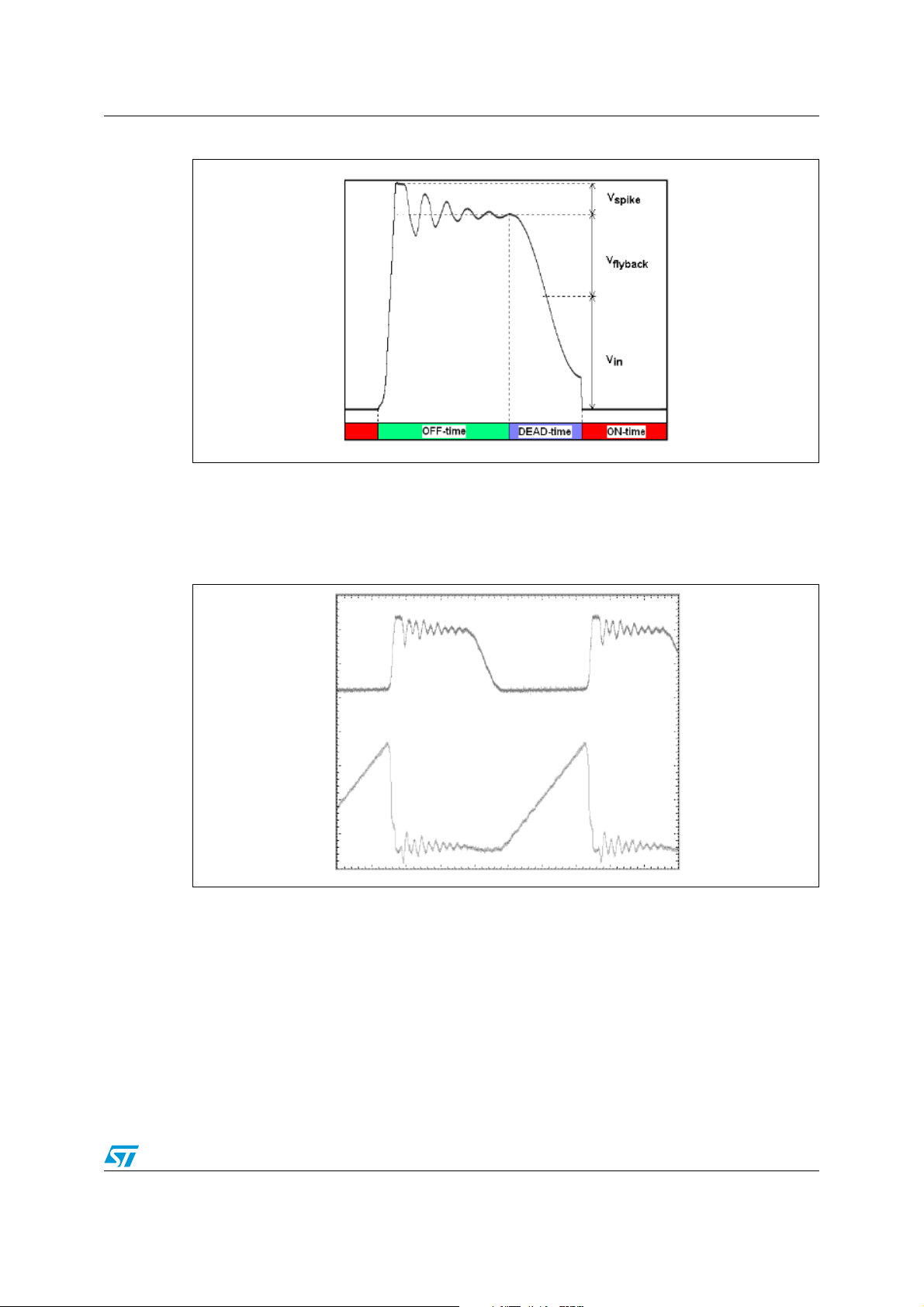
These names come from the waveform shape of the voltage across the primary side switch
during or just before switch turn-on. Figure 1. shows the switch voltage, which is the sum of
V
, the DC bulk capacitor voltage, and V
IN
winding.
The winding voltage depends on the state of the switch and the amount of magnetizing
energy stored in the magnetic circuit of the transformer. One switching period can be divided
into three basic areas determined by the state of the primary switch and the output diode
conduction: the ON time, the OFF time and the DEAD time areas.
● The “ON time” area corresponds to the time during which the primary switch is on and
the transformerfs magnetizing inductance stores energy.
● During the “OFF time”, the primary switch is off and the magnetizing inductance energy
is discharged through the conducting output diode to the output capacitor. A ringing
voltage of amplitude V
also occurs during this phase. It is generated by the layout-
spike
related track inductance and by the leakage inductance created by the imperfect
magnetic field coupling between the transformer primary and secondary windings. The
ringing voltage amplitude is controlled and limited by a clamp circuit.
● The “DEAD time” starts once all the stored magnetizing inductance energy has been
discharged to the output capacitor. It is called “DEAD time” because neither the primary
switch nor the output diode is conducting. So there is no energy transfer between the
primary side and the secondary side. The primary winding voltage during this phase is
resonating and has a cosine waveform starting from a voltage equal to the OFF-time
plateau voltage. The DEAD time is used for the initiation of the next switching cycle,
only there is no energy conversion, which is why this concept is called QUASI resonant,
in comparison with pure resonant converters where the resonance of the primary
current or voltage is the means of energy conversion. The voltage waveform has a
negative slope and approaches or can even cross zero. The suitable moment to turn
the primary switch on again is when the voltage across the primary switch is lowest.
The shape of the switch voltage waveform at this point evokes a valley. This is why
quasi-resonant or zero-voltage switching is also called valley switching. The resonance
frequency during the DEAD time is determined by the magnetizing inductance and
parasitic capacitance. The parasitic capacitance consists of the primary switch
capacitance, the transformer winding capacitance, the inter-winding capacitance, the
capacitances of the diodes located in the secondary, auxiliary and clamp circuits
transformed to the primary side. The PCB tracks also generate some parasitic
capacitance depending on the layout.
, the reflected voltage across the primary
flyback
4/21
Page 5
AN2252 Theory of ESBT and quasi-resonant operation
Figure 1. Flyback converter switching cycle - primary switch voltage
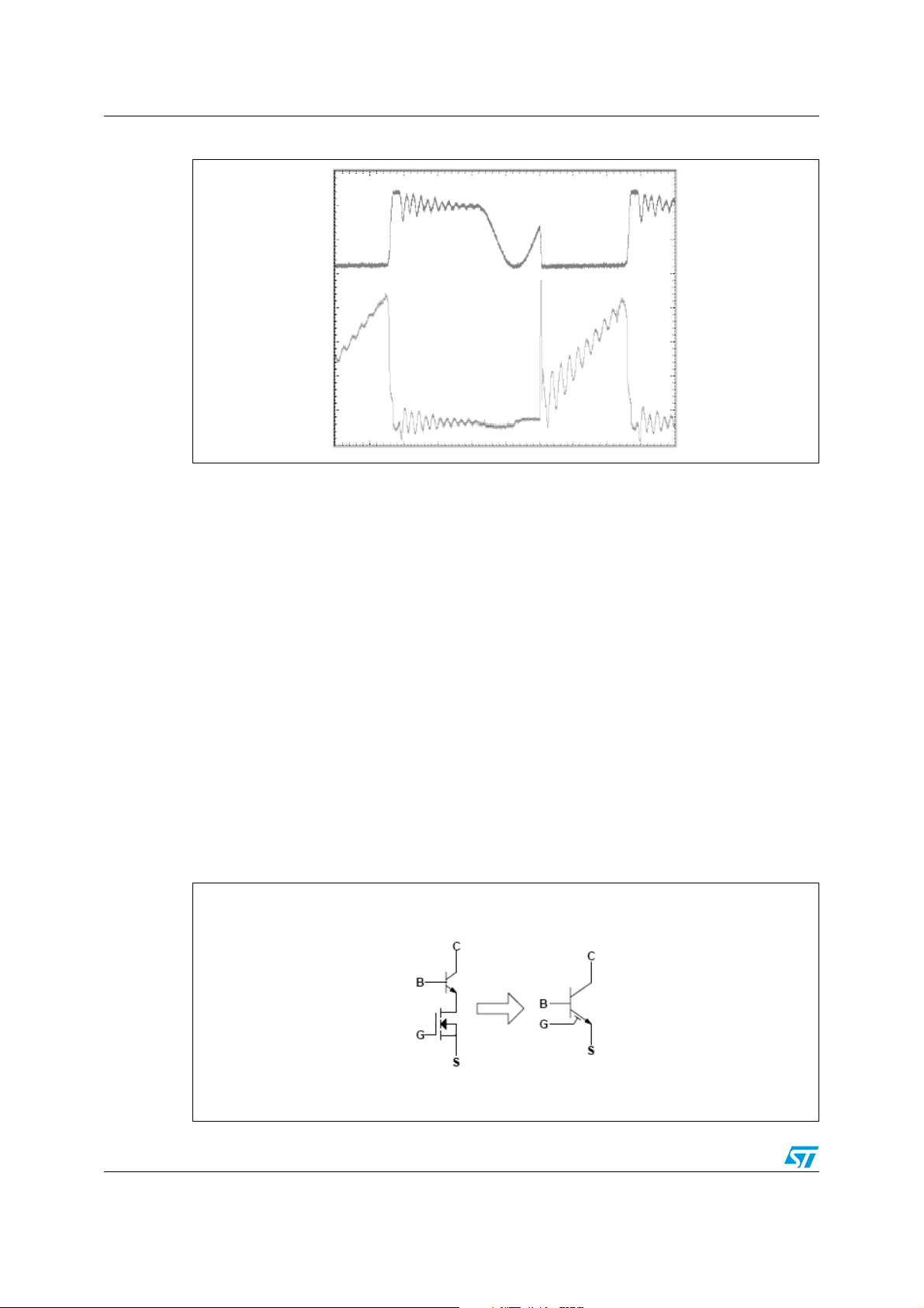
The zero-switching operation mode was selected because it has a higher efficiency and
produces less EMI. The benefits of using zero-voltage turn-on for the primary switch can be
clearly seen by comparing Figure 2. and Figure 4. The switch voltage obtained with zero-
voltage turn-on has a higher waveform and the drain or collector current is lower.
Figure 2. Zero voltage turn-on
5/21
Page 6
Theory of ESBT and quasi-resonant operation AN2252
Figure 3. Non zero voltage turn-on
Beside its advantages, the ZVS mode of operation has challenges. The main challenge lies
in the voltage rating of the primary switch. One of the conditions required for ZVS is that the
voltage across the switch must be able to fall to zero for a certain time during the DEAD
time.
This condition can be met by selecting the V
than DC bulk capacitor voltage V
least twice the maximum V
680VDC, a spike voltage V
IN
spike
. The total voltage across the switch can then reach at
IN
voltage. Considering a double maximum value of VIN of
of 100V plus a safety margin, a switch rated at a minimum of
voltage so that it is equal to or greater
flyback
1500V is required.
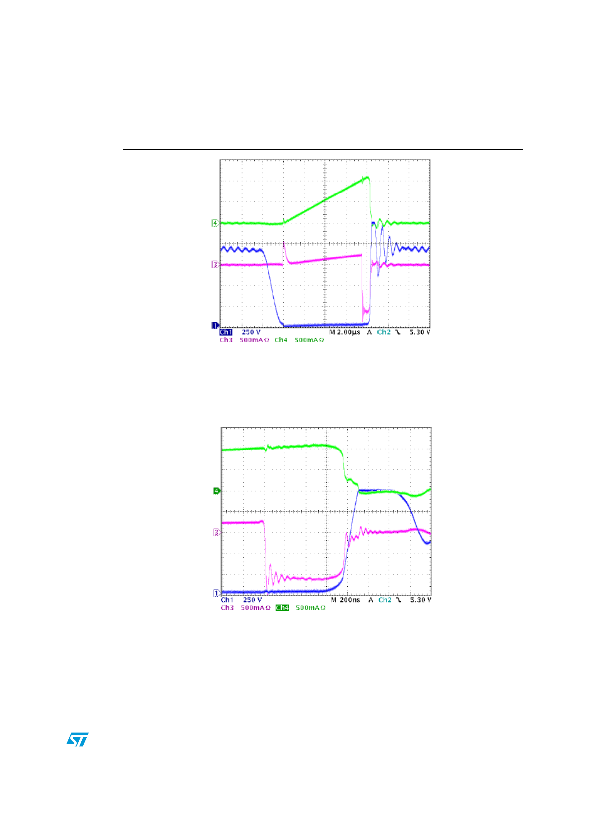
Among the available switches rated for such a high voltage, the high-voltage ESBTs from
STMicroelectronics have a low on-state voltage drop like BJTs, a square safe operating
area, they are easy to drive and have a switching speed comparable to that of MOSFETs.
The ESBT is the cascade configuration of a high-voltage BJT and a low-voltage power
MOSFET, as shown in Figure 5. This configuration is not brand new and its discrete version
is well known. Since STMicroelectronics has a good knowledge and portfolio of high-voltage
BJTs and lowvoltage power MOSFETs with very low drain-source on-state resistances
(Rds-on), the next step was to integrate and optimize the performance of the two devices by
cascading them in a single package to reduce the application complexity, EMI and price,
and to increase reliability.
Figure 4. ESBT’s internal schematic and symbol
6/21
Page 7

AN2252 Application circuit description
Quasi-resonant controller L6565 controls the ESBT by sending a PWM (Pulse Width
Modulation) signal through the gate electrode. The gate electrode drives the internal
lowvoltage MOSFET which switches the emitter of the high-voltage BJT to the external pin S
(source). This is the reason why the transistor is qualified as "emitter switched". The source
pin is usually connected to the application ground.
The base (pin B) of the BJT requires a current bias proportional to the collector current (pin
C). This proportional bias may be provided by a current transformer. The current ratio
between the base and collector currents is given by the current gain h
The current transformer turns ratio must be adapted to the current gain. An example of a
current bias arrangement is given in the Section 2. More details concerning the theoretical
and practical realizations of the bias circuit and the device operation are beyond the scope
of this application note. More details are mentioned in Application Notes AN1699 and
AN1889 (see Section 4), available from the STMicroelectronics website: www.st.com.
of the internal BJT.
21E
2 Application circuit description
2.1 Operating conditions
Table 1. Input/Output specifications
Description Value
Input AC voltage range (400 VAC input) 320 - 480VAC
Input DC voltage range (400 VAC input) 450 - 680VDC
Input AC voltage range (230 VAC input) 160 - 240VAC
Input voltage frequency range 50/60Hz
Nominal output voltage 24VDC
Maximum output current 4.3A
2.2 Circuit operation
Figure 5. shows the schematic of the power supply. The power supply can be supplied from
either an AC or a DC voltage source.
For demonstration purposes in case of an AC supply, power can be supplied through the J2
connector from a single-phase mains of 230VAC. In this case, the input voltage is doubled
by a voltage doubler consisting of diodes D2 and D3, and of capacitors C1 and C2.
If the input voltage source is AC with an RMS value above 240VAC, or if it is a DC source,
the power supply must be connected through connector J1. In this case diodes D2, D3 and
diodes D1, D4 form a bridge rectifier which charges the series-connected capacitors C1 and
C2. In the schematic (Figure 5.), diodes D1, D2, D3, D4 and capacitors C1, C2 are shown
only for demonstration purposes and the converter can be supplied directly from the bus
voltage in the application. The control device is a quasi-resonant controller L6565. During
normal converter operation it is supplied from the auxiliary winding T1C of power
transformer T1 through the one-way rectifier consisting of D5, C4 and C5. Resistor R5 and
7/21
Page 8

Application circuit description AN2252
capacitors C4 and C5 constitute a low-pass filter whose purpose is to reduce the VCC
voltage rise at heavy output loads. At heavy output loads the transformer's parasitic leakage
inductance generates ringing on the auxiliary winding voltage.
Figure 5. Schematic diagram
STC04IE170HV
8/21
Page 9

AN2252 Application circuit description
The VCC capacitors are charged during the start-up phase by the permanent current source
made up of resistors R1, R2 and R3. Thanks to the very low current consumption of L6565
during the start-up phase, the start-up current is in the order of hundreds of microamperes
which significantly reduces the power dissipated in the start-up resistors.
The complete demagnetization of the transformer core is detected by the auxiliary winding
voltage crossing zero. Resistor R6 delivers this information to the IC's internal zero crossing
detector through pin 5. Resistor R7 shifts the zero-crossing detector threshold towards a
value closer to zero for reliable zero crossing during converter start-up or under overload
conditions.
Capacitor C8 delays the power switch turn-on to the moment when the collector voltage
reaches a valley point. The primary current control circuit consists of current-sense resistors
R11, R12 and low-pass filter R9, C7 connected to the CS pin 4 of the control IC.
The primary power switch is the STC04IE170HV. It is an ESBT rated for a maximum current
of 5A and collector-to-source voltage of 1500V. The gate of the ESBT is driven directly by
the internal gate driver of U1 through pin 7. The ESBT also requires a bias current for the
base of the internal BJT. It is provided by current transformer T2 through the diode D7.
During the storage time, the collector current flows through the B-C junction for the time
required by the junction to recover from conduction. The collector current flows then through
capacitor C10 which stores the energy that will generate the initial base current spike
necessary for the next switching cycle. The value of this current spike is determined by the
voltage across capacitor C10 (which is limited by Zener diode D9), by resistor R10 and by
the resistance of the B-E junction of the internal BJT of the ESBT. Diode D6 and resistor R4
provide the bias current required to precharge C10 during the first switching cycle and
properly start the converter operation.
Since the current transformer operation may be affected by core saturation when the
voltsecond product exceeds the limit, a protection circuit consisting of R8, C9, D8 and Q2 is
inserted in the current-sense path. This circuit is a timer which watches the maximum ON
time. If the latter goes beyond a certain limit, the current-sense voltage is suddenly
increased to its maximum threshold, thus stopping the gate driver and turning off the ESBT
through the gate. Without this circuit, the current transformer core saturation would cause
the ESBT to be unsafely turned off whenever there is a lack of base current. This condition
may happen in case of an undervoltage at the input, for instance if a mains voltage drop
occurs or the power supply is unplugged. As a consequence, the ON-time would be
increased above the specified current transformer volt-second product limit.
Clamp circuit D10, D11, C3, R13 and R14 protects the ESBT switch from the voltage spikes
induced by the transformer leakage inductance.
The output voltage is controlled by an opto-isolated feedback loop consisting of U2, voltage
divider R18, R19, R20 and frequency response compensation components R17, C13 and
C14. Since most of the voltage stress was moved (by the increased flyback voltage provided
by an appropriate transformer's turns ratio) to the primary side, a 100V Schottky diode can
be used as a rectifier on the secondary side even if the nominal output voltage is 24V. This is
one of the advantages of using the quasi-resonant mode, which further helps decrease the
output rectifier loss and increases the overall converter power efficiency.
2.2.1 Bill of materials
The list of components required to build the demonstration board is shown in Ta b l e 2 . Most
of the used active components are available from STMicroelectronics. Thanks to the
outstanding performance of the ESBT, the switch does not require any heat sink for this
9/21
Page 10

Application circuit description AN2252
quasi-resonant application delivering a 100W output power. Both inductive components are
supplied by VOGT Electronic Components GmbH.
Table 2. Bill of materials
Referenc
C1,C2 2 150µF Electrolytic capacitor, EPCOS, LL, B43505-A9157-M, 400V
C3 1 6.8nF/1250V Foil capacitor, EPCOS, B32652A7682J
C4 1 10µF Electrolytic capacitor, 25V
C5 2 100nF Ceramic capacitor, 50V, –55 to 125°C
C10 1 100nF/100V Stacked film polyester capacitor, EPCOS, B32560J1104J
C6, C9,
C13
C7 1 470pF Ceramic capacitor, 50V, –55 to 125°C
C8 1 33pF Ceramic capacitor, 50V, –55 to 125°C
C11, C12 2 1000µF/35V Electrolytic capacitor, Panasonic EEUFC1V102, Nichicon UPM1V102MHH6
C14 1 22nF Ceramic capacitor, 50V, –55 to 125°C
D1, D2,
D3, D4
D5, D6,
D7, D8
D9 1 BZX85V3.9 Diode, zener, 3.9V, 1.3W, DO-41
D10, D11 2 STTH108 STMicroelectronics, diode, high voltage ultrafast, 800V, 1A, DO-41
Qty Value Description
e
3 1nF Ceramic capacitor, 50V, –55 to 125°C
4 1N4007 General purpose rectifier, 1000V, 1A, DO-41
4 1N4148 Diode, 75V, 0.15A, DO-35
D12 1 STPS8H100D STMicroelectronics, diode, high voltage power schottky, 100V, 8A, TO-220AC
F1 1 T1A Fuse, radial, SCHURTER, slow, 1A, 250VAC
H1 1 6099B Heatsink, AAVID THERMALOY, 6099B, 531102b02500, Rthjc = 11°C/W
Q1 1 STC04IE170HV
Q2 1 BC547B STMicroelectronics, small signal 100mA, 330mW,TO-92, 150°C
R1, R2,
R3
R4, R9,
R15, R16
R5 1 100 Resistor, size 0204, metal film, 250V, 0.185W, 1%
R6 1 47kΩ Resistor, size 0204, metal film, 250V, 0.185W, 1%
R7 1 390kΩ Resistor, size 0204, metal film, 250V, 0.185W, 1%
R8 1 22kΩ Resistor, size 0204, metal film, 250V, 0.185W, 1%
R10 1 2R2 Resistor, size 0207, metal film, 350V, 0.6W, 1%
R11 1 2.7 Resistor, size 0207, metal film, 350V, 0.6W, 1%
R12 1 2.2 Resistor, size 0207, metal film, 350V, 0.6W, 1%
3 680k Resistor, size 0204, metal film, 250V, 0.185W, 1%
4 1kΩ Resistor, size 0204, metal film, 250V, 0.185W, 1%
STMicroelectronics, Emitter Switched Bipolar Transistor, 4A, 1700V, TO-247
4 leads
10/21
Page 11

AN2252 Application circuit description
Table 2. Bill of materials
Referenc
R13, R14 2 82kΩ Resistor, size 0414, metal film, 500V, 2W, 5%
R17, R20 2 4,7kΩ Resistor, size 0204, metal film, 250V, 0.185W, 1%
R18 1 39kΩ Resistor, size 0204, metal film, 250V, 0.185W, 1%
R19 1 120kΩ Resistor, size 0204, metal film, 250V, 0.185W, 1%
T1 1 SL 040 923 11 03 VOGT-electronic, Power transformer, ETD39, N67
T2 1 SL 040 903 21 02 VOGT-electronic, Current transformer, RM13*7*4.5, Fi 340
U1 1 L6565 STMicroelectronics, quasi-resonant SMPS controller, DIP-8
U2 1 TL431AI
U3 1 PC817 optocoupler, SHARP, Viso = 5kV, CTR = 50..600% at IF = 5mA, DIP-4
Qty Value Description
e
STMicroelectronics, shunt Reference, 2.5V, 1 to 100mA, 2%, TO-91, –40 to
105°C
2.2.2 Transformer design
The initial power transformer specification is as follows:
● Minimum input voltage 320VAC = 450VDC
● Minimum switching frequency at full load and minimum input voltage 50kHz
● Reflected flyback voltage 500V
● Converter efficiency at full load and minimum input voltage 90%
The initial power transformer design was further optimized by VOGT Electronic Components
GmbH to cope with such a high voltage. Special attention was paid to guarantee VDE
distances by padding the winding ends.
To improve magnetic coupling, not only the primary winding but also the secondary was
split. The two primary windings so obtained have half the total number of turns each and are
connected in series while the two secondary windings have the nominal number of turns
and are connected in parallel. The windings are laid out as follows starting from the winding
nearest the core: W1 (Primary 1), W2 (Secondary 1), W3 (Primary 2), W4 (Secondary 2)
and W5 (Auxiliary). The transformer is designed so as to comply with the EN60950 safety
standard for CE certification. If the transformer must be compliant with the UL standard – on
the flammability of isolation material – whose compliance is mandatory for applications
implemented in the USA, then some modifications are required. The transformer’s physical
appearance, dimensions and winding arrangement are shown in Figure 6.
Figure 6. Power transformer dimensions and winding arrangement
11/21
Page 12

Application circuit description AN2252
The basic parameters of the power transformer's ferrite core selected from VOGT's ferrite
materials and shapes are shown in Table 3. The gap size was optimized to meet the current
and inductance requirements necessary to provide the nominal output power over the whole
input voltage range.
Table 3. Power transformer core parameters
Shape ETD39
Material Mf 198
Inductance Factor AL[nH] 132
An overview of the major parameters for each winding can be found in Table 4. Because of
the discontinuous conduction flyback, the winding current has only an AC component, and
so care was taken of minimizing the eddy current loss. For this reason the primary and
secondary windings are made of Litz wire.
Table 4. Power transformer winding parameters
Order Start Pin End Pin
1 1 2 78 4 × 0.2 CuLL 803 × 10
2 9 16 8 20 × 0.2 CuLL 8.4 × 10⁻⁶
3 2 4 78 4 × 0.2 CuLL 803 × 10-6
4 10 15 8 20 × 0.2 CuLL 8.4 × 10⁻⁶
5 7 8 5 0.2 CuLL 3.3 × 10⁻⁶
No. of
turns
Wire diameter
[mm]
Wire material Inductance [H]
-6
As was already mentioned, the ESBT requires a proportional base drive to operate. This
function is provided by current transformer T2. The basic parameters of the current
transformer's ferrite core selected from VOGT's ferrite materials and shapes are given in
Table 5. The physical appearance, dimensions and winding arrangement of the current
transformer are shown in Figure 7.
Figure 7. Current transformer dimensions and winding arrangement
12/21
Page 13

AN2252 Application circuit description
Table 5. Current transformer core parameters
Description Value
Shape R13×7×4.5
Material Fi 340
Inductance Factor A
The number of turns of primary winding W2 was optimized so as to achieve the turns ratio
W2/ W1 at which the current transformer follows the current gain of the ESBT and thus
provides proportional base current bias for the ESBT over the whole specified input voltage
range and output load range. An overview of the major parameters for each winding is given
in Table 6.
Table 6. Current transformer winding parameters
Start Pin End Pin No. of turns Wire diameter [mm] Wire material Inductance [H]
3 5 12 0.355 CuLL 313 × 10
6 1 3 0.355 CuLL 19.6 × 10
2.3 PCB Layout
The PCB is designed as a single-sided board made of FR-4 material with a 70µm copper
plating, solder and silk screen mask. The assembled board contains only throughhole
components. The outline dimensions are 139 x 61mm. The top side of the assembly can be
seen in Figure 8.
Figure 8. Assembly schematic
[nH] 2200
L
-6
-6
Figure 9. represents the PCB layout of the copper connections. The holes for through hole
components are not shown.
13/21
Page 14

Application circuit description AN2252
Figure 9. PCB layout
Figure 10. shows the converter.
Figure 10. Picture of the converter
2.3.1 Evaluation and measurements
The converter was specially designed to have a high power efficiency. Figure 11. shows that
the converter’s output efficiency depends on the input voltage (two marginal values are
taken as example). Since the flyback voltage is not higher than the maximum input voltage,
for some values of the input voltage the conditions under which the converter operates in
ZVS mode are not met and the primary switch turn-on is no longer lossless. This is clearly
seen in Figure 11., where there is a difference in efficiency according to Vin in the medium
and low output power regions. At high output powers, however, the primary switch
conduction loss prevail over the turn-on loss.
14/21
Page 15

AN2252 Application circuit description
Figure 11. Converter efficiency versus output power
The main characteristic of the ZVS control used with the L6565 is that the switching
frequency changes with the load and input voltage. The L6565 has a built-in OFF-time
control block which increases the DEAD time by skipping the valley of the collector voltage
as soon as the OFF time overreaches the internal threshold value. Figure 12. demonstrates
the function of this block and shows that the maximum switching frequency is kept below
120kHz and that, at very low load currents the switching frequency has a value similar to
that at full load. This has a positive impact on the switching loss under light load conditions.
Comparatively for a ZVS control with no valley skipping function, the switching frequency
rises dramatically and has a significant impact on the switching loss.
Figure 12. Converter switching frequency versus output power
Detailed views of waveforms under different operating conditions are shown in Figure 13.,
Figure 14., Figure 15. and Figure 16.. Figure 13. shows the switch collector voltage, gate
voltage and base current stored at minimum input voltage and maximum output load. Zero-
voltage turn-on on the collector voltage occurs when the gate voltage goes High. The
oscilloscope waveform of the base current shows the initial peak provided by capacitor C10,
followed by the current ramp supplied by the current transformer. Since more than one
waveform is shown, the base current is not at a scale that makes it possible to also show the
15/21
Page 16

Application circuit description AN2252
full negative current that flows during the storage time. Only part of it can be seen. The
storage time estimated from Figure 13. is of about 800ns.
Figure 13. Primary switch collector voltage, gate voltage and base current at full
load and minimum input voltage
Note: Channel 1 shows the switch collector voltage (dark blue), channel 2 shows the gate voltage
(light blue) and channel 4 shows the base current (green).
Figure 14. shows the same waveforms as Figure 13. but under maximum input voltage
conditions. Since the flyback voltage is lower than the input voltage, the switch turn-on does
not occur at zero voltage as can be seen from the collector voltage. The storage time
remains the same.
Figure 14. Primary switch collector voltage, gate voltage and base current at full
load and maximum input voltage
Note: Channel 1 shows the switch collector voltage (dark blue), channel 2 shows the gate voltage
(light blue) and channel 4 shows the base current (green).
16/21
Page 17

AN2252 Application circuit description
Figure 15. shows the same waveforms as Figure 13. but at 10% of the specified load. The
storage time is the same as for full load: about 800ns. This proves the good design and
operation of the current transformer that maintains a constant storage time for different
loads and input voltages. Figure 13., Figure 14. and Figure 15. also highlight the valley-
skipping function of the control IC which helps keep the switching frequency within a
reasonable range.
Figure 15. Primary switch collector voltage, gate voltage and base current at 10%
load and minimum input voltage
Note: Channel 1 shows the switch collector voltage (dark blue), channel 2 shows the gate voltage
(light blue) and channel 4 shows the base current (green).
Figure 16. shows that the storage time remains stable even under maximum input voltage
conditions.
Figure 16. Primary switch collector voltage, gate voltage and base current at 10%
load and maximum input voltage
17/21
Page 18

Application circuit description AN2252
Figure 17. shows the principle of the emitter-switching operation of the ESBT. During the
turn-off time the BJT enters the storage time area which can be identified by a negative
base current. The amplitude of the base current during the storage time is equal to the
actual collector current just before gate turn-off. The base-emitter junction is not conducting
and all the collector current flows through the collector-base junction. This process is similar
to the reverse recovery of a standard diode. Since the recovery current is high, the storage
time is very short. The storage time can be easily read from Figure 17. and its value is of
about 800ns. Since the baseemitter junction is not conducting, current crowding and hot-
spot effects are greatly reduced, which gives rise to an excellent square Reverse Bias Safe
Operating Area (RBSOAR) similar to the Safe Operating Area (SOAR) of power MOSFETS.
Figure 17. Detailed view of the primary switch base current
Figure 18. shows the part of the base current waveform that corresponds to the storage
time. Collector voltage is also represented. The Collector voltage rise indicates where
storage finishes and the current fall time begins.
Figure 18. Detailed view of the primary switch base current
Note: Channel 4 shows the base current (green) and channel 1 shows the collector voltage (blue).
18/21
Page 19
AN2252 Application circuit description
Figure 19. highlights the proportional drive. It shows the collector current (channel 4 - green)
and the base current (channel 3 - pink) at the same scale. Channel 1 (blue) is the collector
voltage.
Figure 19. Proportional base current
Figure 20. shows how the base current copies the collector current during the storage time
and the current fall time. Channel 4 shows the collector current (green), channel 3 shows the
base current (pink) and Channel 1 shows the collector voltage (blue).
Figure 20. Detailed proportional base and collector current
Table 7. shows the results of the case temperature measurement of the primary ESBT
switch and secondary Schottky diode at a 25°C room temperature, for full power and two
marginal input voltage values.
19/21
Page 20

Conclusion AN2252
Table 7. Temperatures of the power switches at full load
Input voltage [VDC] ESBT temperature [°C] Diode D12 temperature [°C]
450 80.5 82
620 79.7 80.2
Note that the ESBT switch does not have any external heat sink attached to its case. The
other most heating elements and sources of loss are the mains transformer and output
capacitors. Even when the loss generated by these passive components is minimized by a
suitable component selection and a good design, they are still significant overall converter
loss sources.
3 Conclusion
This application note shows how to build a high-input voltage power supply operating in
quasiresonant mode. The obtained efficiency is around the target value and can be further
improved by introducing a synchronous rectifier in the place of the secondary diode. With its
high speed, low conduction loss and low turn-on loss, the ESBT does not need a heatsink to
be used as a primary switch.
As this power supply is designed for use as an auxiliary supply, and only part of the
application is supplied from its input bulk capacitor, the EMI filter was not accommodated on
the board and the power supply was not tested for EMC compliance.
4 References
● AN1699, “Efficient driving network for ESBT to reduce the dynamic V
enhance the switching performances”
● AN1889, “ESBT STC03DE170 IN 3-PHASE AUXILIARY POWER SUPPLY”
5 Revision history
Table 8. Revision history
Date Revision Changes
Dec-2005 1 First issue
28-Nov-2006 2
- The document has been reformatted
- Table 2. and Figure 5. modified
CESAT
and
20/21
Page 21

AN2252
Please Read Carefully:
Information in this document is provided solely in connection with ST products. STMicroelectronics NV and its subsidiaries (“ST”) reserve the
right to make changes, corrections, modifications or improvements, to this document, and the products and services described herein at any
time, without notice.
All ST products are sold pursuant to ST’s terms and conditions of sale.
Purchasers are solely responsible for the choice, selection and use of the ST products and services described herein, and ST assumes no
liability whatsoever relating to the choice, selection or use of the ST products and services described herein.
No license, express or implied, by estoppel or otherwise, to any intellectual property rights is granted under this document. If any part of this
document refers to any third party products or services it shall not be deemed a license grant by ST for the use of such third party products
or services, or any intellectual property contained therein or considered as a warranty covering the use in any manner whatsoever of such
third party products or services or any intellectual property contained therein.
UNLESS OTHERWISE SET FORTH IN ST’S TERMS AND CONDITIONS OF SALE ST DISCLAIMS ANY EXPRESS OR IMPLIED
WARRANTY WITH RESPECT TO THE USE AND/OR SALE OF ST PRODUCTS INCLUDING WITHOUT LIMITATION IMPLIED
WARRANTIES OF MERCHANTABILITY, FITNESS FOR A PARTICULAR PURPOSE (AND THEIR EQUIVALENTS UNDER THE LAWS
OF ANY JURISDICTION), OR INFRINGEMENT OF ANY PATENT, COPYRIGHT OR OTHER INTELLECTUAL PROPERTY RIGHT.
UNLESS EXPRESSLY APPROVED IN WRITING BY AN AUTHORIZED ST REPRESENTATIVE, ST PRODUCTS ARE NOT
RECOMMENDED, AUTHORIZED OR WARRANTED FOR USE IN MILITARY, AIR CRAFT, SPACE, LIFE SAVING, OR LIFE SUSTAINING
APPLICATIONS, NOR IN PRODUCTS OR SYSTEMS WHERE FAILURE OR MALFUNCTION MAY RESULT IN PERSONAL INJURY,
DEATH, OR SEVERE PROPERTY OR ENVIRONMENTAL DAMAGE. ST PRODUCTS WHICH ARE NOT SPECIFIED AS "AUTOMOTIVE
GRADE" MAY ONLY BE USED IN AUTOMOTIVE APPLICATIONS AT USER’S OWN RISK.
Resale of ST products with provisions different from the statements and/or technical features set forth in this document shall immediately void
any warranty granted by ST for the ST product or service described herein and shall not create or extend in any manner whatsoever, any
liability of ST.
ST and the ST logo are trademarks or registered trademarks of ST in various countries.
Information in this document supersedes and replaces all information previously supplied.
The ST logo is a registered trademark of STMicroelectronics. All other names are the property of their respective owners.
© 2006 STMicroelectronics - All rights reserved
STMicroelectronics group of companies
Australia - Belgium - Brazil - Canada - China - Czech Republic - Finland - France - Germany - Hong Kong - India - Israel - Italy - Japan -
Malaysia - Malta - Morocco - Singapore - Spain - Sweden - Switzerland - United Kingdom - United States of America
www.st.com
21/21
 Loading...