

Page 1

AN2206
Application note
Designing with L6920DB, high efficiency
syncronous rectifier step-up converter
Introduction
The L6920DB is a high efficiency monolithic step-up switching converter IC especially
designed for battery powered applications, thanks to its minimum start-up of 0.8 V, and a
minimum operating voltage of 0.6 V.
It requires only three external components to realize the conversion from battery voltage to
the selected output voltage.
It has a minimum output voltage of 1.8 V, which is enough to supply even the most advanced
ASICs and microprocessors. The high switching frequency allows users to choose small
inductors and output capacitors for their designs. Supervisory functions include Reference
Voltage, Low Battery Detection, and Shutdown, which are provided with overcurrent
protection.
March 2007 Rev 4 1/11
www.st.com
Page 2

Contents AN2206
Contents
1 Application information . . . . . . . . . . . . . . . . . . . . . . . . . . . . . . . . . . . . . . 3
1.1 Output voltage selection . . . . . . . . . . . . . . . . . . . . . . . . . . . . . . . . . . . . . . . 4
1.2 Input capacitor selection . . . . . . . . . . . . . . . . . . . . . . . . . . . . . . . . . . . . . . . 4
1.3 Output capacitor selection . . . . . . . . . . . . . . . . . . . . . . . . . . . . . . . . . . . . . 4
1.4 Inductor selection . . . . . . . . . . . . . . . . . . . . . . . . . . . . . . . . . . . . . . . . . . . . 5
1.5 Switching frequency . . . . . . . . . . . . . . . . . . . . . . . . . . . . . . . . . . . . . . . . . . 5
1.6 Low battery detection . . . . . . . . . . . . . . . . . . . . . . . . . . . . . . . . . . . . . . . . . 5
1.7 Layout guidelines . . . . . . . . . . . . . . . . . . . . . . . . . . . . . . . . . . . . . . . . . . . . 7
2 Typical performance . . . . . . . . . . . . . . . . . . . . . . . . . . . . . . . . . . . . . . . . . 9
3 Revision history . . . . . . . . . . . . . . . . . . . . . . . . . . . . . . . . . . . . . . . . . . . 10
2/11
Page 3
AN2206 Application information
1 Application information
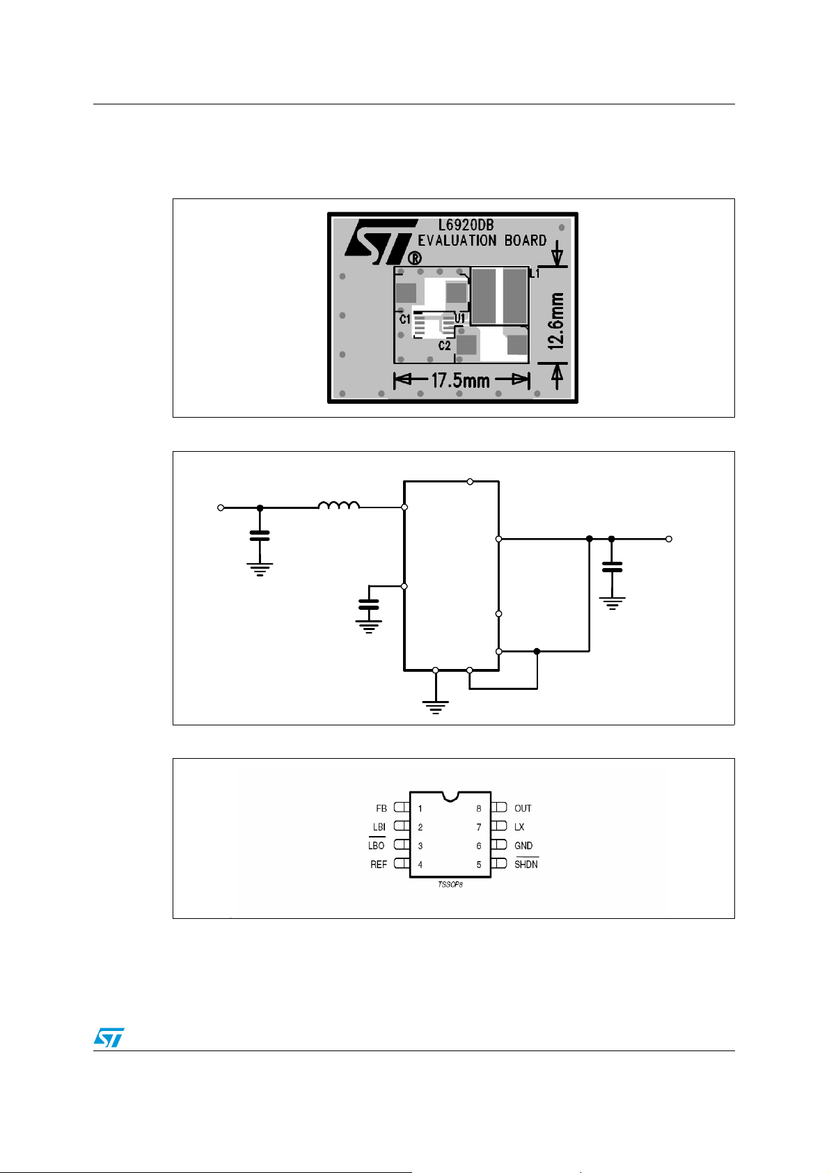
Figure 1. L6920DB Example of overall application size
Figure 2. Application circuit
LBI
V
=2.5V
BATT
L1 10µH
C1
47µF
100nF
LX
V
REF
C4
4
GND
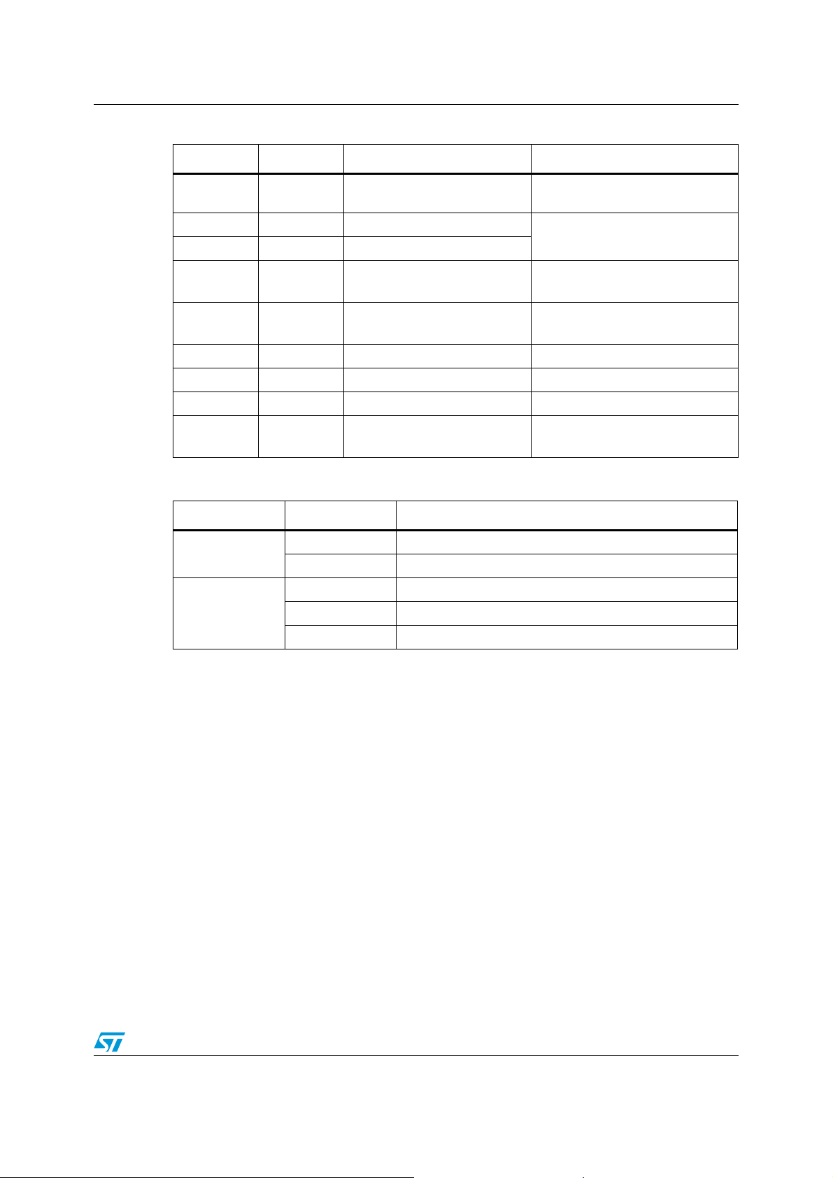
Figure 3. Pin connections (top view)
7
L6920D
6
2
5
8
3
1
_____
SHDN
V
___
LBO
FB
OUT
C1
47µF
=3.3V
V
OUT
3/11
Page 4
Application information AN2206
1.1 Output voltage selection
The output voltage must be selected by configuring the FB pin. Three choices are available:
● fixed 3.3 V
● fixed 5 V
● adjustable output set via an external resistor divider.
R4 and R5 should be selected in the range of 100 kΩ - 1 MΩ to minimize power consumption
and errors due to current sunk by FB pin (a few nA). See Figure 5
Table 1. Output voltage connection
Output voltage Feedback connection
=3.3 V FB Connected to OUT (See Figure 5)
V
OUT
V
=5 V FB Connected to GND (See Figure 5)
OUT
FB Connected to a resistor divider
R4
1.8 V=V
OUT
=5.2 V
V
OUT
1.23V 1
⎛⎞
------- -+
•=
⎝⎠
R5
1.2 Input capacitor selection
A minimum capacitance is usually added at the input to filter the current ripple. 10 µF are
enough for most of the applications.
Low-ESR Tantalum and Multilayer Ceramic Capacitors (MLCC) are good choices.
1.3 Output capacitor selection
The output capacitor affects both efficiency and output ripple, so its choice has to be
considered with particular care. The capacitance value should be in the range of about
10mF-100 µF. An additional, smaller, low Equivalent Series Resistance (ESR) capacitor can
be used (not mandatory) in parallel for high frequency filtering. A typical value is around
1 µF.
Note: For very high performance requirements (e.g., efficiency and output voltage ripple), a very
low ESR capacitor has to be used (e.g. MLCC capacitors).
Other possibilities include low-ESR tantalum capacitors, available from KEMET, and other
sources. POSCAP capacitors from SANYO and polymeric capacitors from PANASONIC are
also good choices (see Ta b l e 2 ).
Note: The cap values and rated voltages are only suggested possibilities.
Table 2. Distributor's capacitor main list
Manufacturer Series Cap value (µF) Rated voltage (V) ESR (mΩ)
KEMET T510/T494/ T495 10 to 47 6 30 to 100
4/11
Page 5

AN2206 Application information
Table 2. Distributor's capacitor main list (continued)
Manufacturer Series Cap value (µF) Rated voltage (V) ESR (mΩ)
PANASONIC EEFCD 22 to 47 6.3 50 to 700
SANYO POSCAP TPA/B/C 22 to 230 6.3 40 to 80
1.4 Inductor selection
Usually, inductors ranging between 2 µH to 10 µH satisfy most application requirements.
However, small-value inductors are physically smaller and guarantee a faster response to
load transients.
Inductor size also affects the maximum current deliverable to the load. A low series
resistance is suggested if very high efficiency values are needed. In any case, the saturation
current of the choke should be higher than the peak current limit of the device (800 mA typ.).
Good surface-mount inductors are available from COILCRAFTS, COILTRONICS and other
sources (see Ta bl e 3 ).
Table 3. Distributor's inductor main list
Manufacturer Series Inductor value (µH) Saturation current (A)
Coilcraft
Coiltronics
Panasonic
LPO1704 2.2 to 10 0.9 to 1.6
LPO6610 2.2 to 10 0.9 to 1.5
ELL6SH 10 to 22 0.9 to 1.5
ELL6RH 5.1 to10 1.1 to 1.55
1.5 Switching frequency
The control loop of the L6920DB is based on a Minimum OFF-time and a Maximum ON-time
(see datasheet). This means that the switching frequency is not fixed, but changes in order
to keep the output voltage regulated. The maximum reachable value is approximately 1MHz.
The frequency value depends on the inductor value, input and output voltage, and the load.
1.6 Low battery detection
The L6920DB includes a low battery detection comparator. The threshold is V
and a hysteresis is added to avoid oscillations when input crosses the threshold slowly. The
Low Battery Output (LBO
use. Adding a resistor divider at the Low Battery Input (LBI) pin gives the user the ability to
set at which value of V
) is an open drain, so a pull-up resistor, R3, is required for proper
the (LBO goes high. The relationship is showed below:
BATT
SD10 2.2 to 6.2 0.9 to 1.6
SD12 3.3 to 10 0.85 to 1.4
voltage
REF
Equation 1
V
BATT TH–
1.23V 1
⎛⎞
•=
⎝⎠
R1
--------+
R2
5/11
Page 6

Application information AN2206
L1 10
µ
If a Low battery voltage detection than 1.23 V is required, it is possible using a resistor
divider between V
OUT
and V
, showed in the Figure 4.
BATT
In this case the relationship is the following:
Equation 2
V
BATT TH–
1.23
V
⎛⎞
---------------------------------
⎝⎠
OUT
1.23–
R
R
2
1•–=
In order to keep the efficiency high, the resistors of this divider must be chosen with a value
higher than 100 KΩ.
Figure 4. Schematic for low battery voltage detection below the 1.23 V voltage
reference
Figure 5. Demoboard schematic
V
BATT
N.C
C4
100nF
R1
N.C
R2
LBI
V
REF
GND
2
L6920D
4
6
LX
FB
7
V
OUT
8
R3
N.C
___
LBO
3
_____
SHDN
5
1
H
J1
1
2
3
1
2
3
Table 4. Demo board components description
J2
C3
N.C
R4 N.C.
R5 N.C.
C2
47µF
C1
47µF
V
BATT
GND
V
OUT
GND
___
LBO
_____
SHDN
Name Value Manufacturer Description
R1 N.C
Low battery Input resistor divider
R2 N.C
6/11
Page 7
AN2206 Application information
Table 4. Demo board components description (continued)
Name Value Manufacturer Description
R3 N.C
R4 N.C
R5 N.C
C1 47 µ
C2 47 µ
C3 1 µ
C4 100
U1 L6920DB
L1 10 µH
F
F
F High frequency filter capacitor
nF V
PANASONIC
EEFCDJ470R
PANASONIC
EEFCDJ470R
PANASONIC
ELL6RH100M
Table 5. Jumper connections
Jumper Position Function
J1
1-2 Device enabled
2-3 Device disabled
None Adjustable using R4 and R5 (not mounted)
Pull-up resistor. Connected
between VOUT and LBO pins.
Output voltage resistor divider
Output capacitor
Input capacitor
filter capacitor
REF
Inductor
J2
1.7 Layout guidelines
The board layout is very important in order to minimize noise, high frequency resonance
problems and electromagnetic interference. It is essential to keep the high switching current
circulating paths as small as possible to reduce radiation and resonance problems. The
output and input cap should be very close to the device.
The external resistor dividers, if used, should be as close as possible to the FB and LBI pins
of the device, and as far as possible from the high current circulating paths, to avoid pick-up
noise.
Large traces for high current paths and an extended ground plane help reduce noise and
increase the efficiency.
For an example of recommended layout see the following evaluation board.
1-2 3.3 V output voltage
2-3 5 V output voltage
7/11
Page 8

Application information AN2206
Figure 6. Demoboard layout (top view)
Figure 7. Demoboard layout (bottom view)
8/11
Page 9

AN2206 Typical performance
2 Typical performance
Figure 8. Efficiency vs. output current at Vout = 3.3 V
Figure 9. Efficiency vs. output current at Vout = 5 V
Figure 10. Start-up voltage vs. output current at Vout = 5 V
VStart up vs. output current
1600
1500
1400
1300
1200
1100
1000
VStart up (mV
900
800
700
600
0.1 1 10 100 1 00 0
Output current (mA)
9/11
Page 10

Revision history AN2206
Figure 11. Start-up voltage vs. output current at Vout = 3.3 V
VStart up vs. output curren t
1600
Vout=3.3V
1500
1400
1300
1200
1100
1000
VStart up (mV
900
800
700
600
0.1 1 10 100 1000
Output current (mA)
3 Revision history
Table 6. Revision history
Date Revision Changes
05-Dec-2005 1 First issue
09-Feb-2006 2 Text modification
- New template
05-Oct-2006 3
26-Mar-2007 4 - Ta b le 4 modified
- Equation 2 modified
- Figure 4 modified
10/11
Page 11

AN2206
Please Read Carefully:
Information in this document is provided solely in connection with ST products. STMicroelectronics NV and its subsidiaries (“ST”) reserve the
right to make changes, corrections, modifications or improvements, to this document, and the products and services described herein at any
time, without notice.
All ST products are sold pursuant to ST’s terms and conditions of sale.
Purchasers are solely responsible for the choice, selection and use of the ST products and services described herein, and ST assumes no
liability whatsoever relating to the choice, selection or use of the ST products and services described herein.
No license, express or implied, by estoppel or otherwise, to any intellectual property rights is granted under this document. If any part of this
document refers to any third party products or services it shall not be deemed a license grant by ST for the use of such third party products
or services, or any intellectual property contained therein or considered as a warranty covering the use in any manner whatsoever of such
third party products or services or any intellectual property contained therein.
UNLESS OTHERWISE SET FORTH IN ST’S TERMS AND CONDITIONS OF SALE ST DISCLAIMS ANY EXPRESS OR IMPLIED
WARRANTY WITH RESPECT TO THE USE AND/OR SALE OF ST PRODUCTS INCLUDING WITHOUT LIMITATION IMPLIED
WARRANTIES OF MERCHANTABILITY, FITNESS FOR A PARTICULAR PURPOSE (AND THEIR EQUIVALENTS UNDER THE LAWS
OF ANY JURISDICTION), OR INFRINGEMENT OF ANY PATENT, COPYRIGHT OR OTHER INTELLECTUAL PROPERTY RIGHT.
UNLESS EXPRESSLY APPROVED IN WRITING BY AN AUTHORIZED ST REPRESENTATIVE, ST PRODUCTS ARE NOT
RECOMMENDED, AUTHORIZED OR WARRANTED FOR USE IN MILITARY, AIR CRAFT, SPACE, LIFE SAVING, OR LIFE SUSTAINING
APPLICATIONS, NOR IN PRODUCTS OR SYSTEMS WHERE FAILURE OR MALFUNCTION MAY RESULT IN PERSONAL INJURY,
DEATH, OR SEVERE PROPERTY OR ENVIRONMENTAL DAMAGE. ST PRODUCTS WHICH ARE NOT SPECIFIED AS "AUTOMOTIVE
GRADE" MAY ONLY BE USED IN AUTOMOTIVE APPLICATIONS AT USER’S OWN RISK.
Resale of ST products with provisions different from the statements and/or technical features set forth in this document shall immediately void
any warranty granted by ST for the ST product or service described herein and shall not create or extend in any manner whatsoever, any
liability of ST.
ST and the ST logo are trademarks or registered trademarks of ST in various countries.
Information in this document supersedes and replaces all information previously supplied.
The ST logo is a registered trademark of STMicroelectronics. All other names are the property of their respective owners.
© 2007 STMicroelectronics - All rights reserved
STMicroelectronics group of companies
Australia - Belgium - Brazil - Canada - China - Czech Republic - Finland - France - Germany - Hong Kong - India - Israel - Italy - Japan -
Malaysia - Malta - Morocco - Singapore - Spain - Sweden - Switzerland - United Kingdom - United States of America
www.st.com
11/11
 Loading...