

Page 1
AN2200
APPLICATION NOTE
Guidelines for migrating ST7LITE1x applications to ST7FLITE1xB
Introduction
This application note provides information on migrating ST7FLITE1x-based applications to
ST7FLITE1xB.
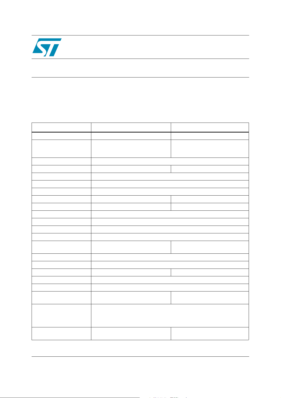
Table 1. Feature comparison
ST7FLITE1x ST7FLITE1xB
Package SO20 300 SO20 300"/ DIP20/ SO16 300" /DIP16
ST7LITE10
Device Name
Program Memory 4K (No change)
Operating Supply 2.4V to 5.5V 2.7V to 5.5V
Operating Temperature -40°C to 85°C (No change)
RAM (stack) - bytes 256 (128) (No change)
Data EEPROM - bytes 128 (No change)
I/Os 15, PA7:0, PB6:0 17, PA7:0, PB6:0, PC1:0
Interrupt 10 12
Power saving modes Slow, Wait, Active Halt, AWUFH, Halt (No change)
Clock Source 1% Internal RC, PLLx4/8, External clock source, Crystal, Resonator oscillator,
Lite Timer Yes (no change)
Watchdog Timer Yes (no change)
12-bit Autoreload Timer
with 32 MHz input clock
SPI Yes (no change)
10-bit ADC with Op-Amp Yes (no change)
Analog Comparator No Yes
Emulator ST7MDT10-EMU3 (No change)
ST7 DVP3 Series ST7MDT10-DVP3(No change)
Programming tools (EPB) ST7MDT10-EPB
Programming tools
(Socket Board)
ICD Tool
INDART kit (Softec) and Reva kit
ST7LITE15
ST7LITE19
Ye s
(Raisonance)
Yes with two counters, one pulse mode,
ST7MDT10-EPB (only for SO20
ST7SB10-123/EU
ST7SB10-123/US
ST7SB10-123/UK
(to be used along with STICK)
ST7LITE10B
ST7LITE15B
ST7LITE19B
dead time
package)
Reva kit (Raisonance)
Rev 1
July 2005 1/13
www.st.com
13
Page 2

Migrating applications from ST7FLITE1x to ST7FLITE1xB
Contents
1 Feature Overview . . . . . . . . . . . . . . . . . . . . . . . . . . . . . . . . . . . . . . . . . . . . . . 3
2 Pinout compatibility . . . . . . . . . . . . . . . . . . . . . . . . . . . . . . . . . . . . . . . . . . . 4
2.1 Package . . . . . . . . . . . . . . . . . . . . . . . . . . . . . . . . . . . . . . . . . . . . . . . . . . . . . 4
2.2 SO20 pinout . . . . . . . . . . . . . . . . . . . . . . . . . . . . . . . . . . . . . . . . . . . . . . . . . . 4
3 Register map . . . . . . . . . . . . . . . . . . . . . . . . . . . . . . . . . . . . . . . . . . . . . . . . . 5
3.1 Register address . . . . . . . . . . . . . . . . . . . . . . . . . . . . . . . . . . . . . . . . . . . . . . . 5
3.2 Register content differences . . . . . . . . . . . . . . . . . . . . . . . . . . . . . . . . . . . . . . 7
3.2.1 SICSR register . . . . . . . . . . . . . . . . . . . . . . . . . . . . . . . . . . . . . . . . . . . . . . . . 7
3.2.2 PWMxCSR Register . . . . . . . . . . . . . . . . . . . . . . . . . . . . . . . . . . . . . . . . . . . . 7
3.2.3 BREAKCR Register . . . . . . . . . . . . . . . . . . . . . . . . . . . . . . . . . . . . . . . . . . . . . 7
3.2.4 TRANCR Register . . . . . . . . . . . . . . . . . . . . . . . . . . . . . . . . . . . . . . . . . . . . . . 8
4 New features in ST7FLITE1xB . . . . . . . . . . . . . . . . . . . . . . . . . . . . . . . . . . . 9
4.1 Clock management . . . . . . . . . . . . . . . . . . . . . . . . . . . . . . . . . . . . . . . . . . . . . 9
4.2 12-bit autoreload timer . . . . . . . . . . . . . . . . . . . . . . . . . . . . . . . . . . . . . . . . . . 9
4.2.1 Dual counters . . . . . . . . . . . . . . . . . . . . . . . . . . . . . . . . . . . . . . . . . . . . . . . . . 9
4.2.2 Break function . . . . . . . . . . . . . . . . . . . . . . . . . . . . . . . . . . . . . . . . . . . . . . . . . 9
4.2.3 Dead time generation . . . . . . . . . . . . . . . . . . . . . . . . . . . . . . . . . . . . . . . . . . 10
4.2.4 Long input capture . . . . . . . . . . . . . . . . . . . . . . . . . . . . . . . . . . . . . . . . . . . . . 10
4.2.5 One pulse mode . . . . . . . . . . . . . . . . . . . . . . . . . . . . . . . . . . . . . . . . . . . . . . 10
4.2.6 Forced update . . . . . . . . . . . . . . . . . . . . . . . . . . . . . . . . . . . . . . . . . . . . . . . . 10
4.3 Analog comparator . . . . . . . . . . . . . . . . . . . . . . . . . . . . . . . . . . . . . . . . . . . . 10
4.3.1 On-chip analog comparator . . . . . . . . . . . . . . . . . . . . . . . . . . . . . . . . . . . . . . 10
4.3.2 Programmable internal voltage reference . . . . . . . . . . . . . . . . . . . . . . . . . . . 10
5 Electrical characteristics . . . . . . . . . . . . . . . . . . . . . . . . . . . . . . . . . . . . . . 11
6 Device ordering information . . . . . . . . . . . . . . . . . . . . . . . . . . . . . . . . . . . . 13
2/13
Page 3
Migrating applications from ST7FLITE1x to ST7FLITE1xB 1 Pinout compatibility
1 Pinout compatibility
1.1 Package
ST7FLITE1x is available only in SO20 300” package. ST7FLITE1xB is available in SO20 300”,
DIP20, SO16 300” and DIP16 packages.
1.2 SO20 pinout
Both ST7FLITE1x and ST7FLITE1xB are pin to pin compatible. On some pins of ST7FLITE1xB
new alternate functions have been added to add new peripherals/ features.
ST7FLITE1x ST7FLITE1xB
Pin No. 4 SS
/AIN0/PB0
Pin No. 8 CLKIN/AIN4/PB4
Pin No. 11 PA 7
Pin No. 19 OSC2
Pin No. 20 OSC1/CLKIN
COMPIN+
COMPIN-
(1)
/SS/AIN0/PB0
(2)
/CLKIN/AIN4/PB4
PA 7/ COMPOUT
OSC2/PC1
(4)
OSC1/CLKIN/PC0
(3)
(5)
(1)
COMPIN+: Analog Comparator Input
(2)
COMPIN-: Analog Comparator External Reference Input
(3)
COMPOUT: Analog Comparator Output
(4)
PC1: Port C1
(5)
PC2: Port C2
3/13
Page 4

2 Register map Migrating applications from ST7FLITE1x to ST7FLITE1xB
2 Register map
In ST7FLITE1xB, some register addresses have been added, some modified to add new
features and peripherals.
Note: For easy software migration, two general rules to be followed:
All “reserved” byte memory areas must never be “read” or “write”.
All “reserved” and “unused” bits must be left unchanged when accessing the byte.
2.1 Register address
These changes are classified in two groups:
1. New features added: Port C, dual counters in ART Timer, one pulse mode, External Break,
Dead Time generation, Force Update in ART Timer, Analog Comparator and PLL divider.
2. TRANCR (Transfer Control Register) has been replaced by ATCSR2 (Timer Control
Register2). Seven bits relative to the new features in ART Timer have been added in
ATCSR2 register. TRAN <bit0> of TRANCR register has been replaced by TRAN1 <bit0>.
Please, refer to the datasheet for the detailed description of the new features.
4/13
Page 5

Migrating applications from ST7FLITE1x to ST7FLITE1xB 2 Register map
Figure 1. Register map modifications
ST7FLITE1x
@Block
0006h
0007h
000Dh
000Eh CNTRH
000Fh CNTRL
0010h ATRH
0011h ATRL
0012h PWMCR
0013h PWM0CSR
0014h PWM1CSR
0015h PWM2CSR
0016h PWM3CSR
Autore-
0017h DCR0H
load Tim-
0018h DCR0L
0019h DCR1H
001Ah DCR1L
001Bh DCR2H
001Ch DCR2L
001Dh DCR3H
001Eh DCR3L
001Fh ATICRH
0020h ATICRL
0021h TRANCR
0022h BREAKCR
0023h
0024h
0025h
0026h
er 2
Register
Label
Reserved Area
ATCSR
Reserved Area
ST7FLITE1xB
@Block
0006h Port C PCDR
1
0007h Port C PCDDR
000Dh
000Eh CNTRH
000Fh CNTRL
0010h ATRH
0011h ATRL
0012h PWMCR
0013h PWM0CSR
0014h PWM1CSR
0015h PWM2CSR
0016h PWM3CSR
0017h DCR0H
0018h DCR0L
0019h DCR1H
Autoreload
001Ah DCR1L
001Bh DCR2H
001Ch DCR2L
001Dh DCR3H
001Eh DCR3L
001Fh ATICRH
2
0020h ATICRL
0021h ATCSR2
0022h BREAKCR
0023h ATR2H
0024h ATR2H
1
0025h DTGR
0026h BREAKEN
Timer 2
Register
Label
ATCSR
002Ch
002Dh
003Bh Reserved Area
004Bh
004Ch DMSR
004Dh DMBK1H
004Eh DMBK1L
004Fh DMBK2H
0050h DMBK2L
0051h Reserved Area
Reserved Area
DMCR
Debug
Module
002Ch
1
002Dh CMPCR
1
003Bh PLL PLLTST
004Bh
004Ch DMSR
004Dh DMBK1H
004Eh DMBK1L
004Fh DMBK2H
0050h DMBK2L
1
0051h DMCR2
Analog
Comparator
Debug Mod-
VREFCR
DMCR
ule
5/13
Page 6

2 Register map Migrating applications from ST7FLITE1x to ST7FLITE1xB
2.2 Register content differences
2.2.1 SICSR register
In the SICSR (System Integrity Control/Status Register) three new bits have been added (see
Figure 2).
LOCK32: It is set when PLL 32 MHz reaches its operating frequency
CR[1:0]: RC Oscillator Frequency Adjustment bits: These bits, as well as CR[9:2] in the RCCR
RC oscillator frequency and to obtain an accuracy of 1%. 10 bits are used for calibration of
Internal RC when compared to 8 bits in ST7FLITE1x.
Figure 2. SICSR Register
ST7FLITE1x ST7FLITE1xB
2.2.2 PWMxCSR Register
In the PWMxCSR (PWMx Control Status Register) two new bits have been added (see Figure
3) corresponding to the One Pulse mode of the Auto reload Timer.
Figure 3. PWMxCSR Register
ST7FLITE1x ST7FLITE1xB
2.2.3 BREAKCR Register
In the BREAKCR (Break Control Register) two new bits have been added (see Figure 4) related
to Break Input Select (External break pin or the output of the comparator) and Break Input Edge
selection.
Figure 4. BREAKCR Register
ST7FLITE1x ST7FLITE1xB
6/13
Page 7

Migrating applications from ST7FLITE1x to ST7FLITE1xB 2 Register map
2.2.4 TRANCR Register
The TRANCR (Transfer Control Register) has been replaced by ATCSR2 (Timer Control
Register2) (see Figure 5). ATCSR2 contains bits related to the additional features of the Auto
Reload Timer i.e. Dual counters, Forced update, Long Input Capture
Figure 5. TRANCR Register Changes
ST7FLITE1x (TRANCR) ST7FLITE1xB (ATCSR2)
7/13
Page 8

3 New features in ST7FLITE1xB Migrating applications from ST7FLITE1x to ST7FLITE1xB
3 New features in ST7FLITE1xB
3.1 Clock management
Some changes have been made in the clock management. They are as follows:
1. It is possible to also run at 4MHz with RC and PLL from 2.7V to 5.5V. An additional
PLLTST register is available in ST7FLITE1xB containing the PLLDIV2 bit which allows you
to divide the PLL output clock by 2. Hence, x4 PLL (x4PLL from 2.7V to 3.3V and x8PLL /
2 from 3.3V to 5.5V) is effectively available for the entire operating voltage range of the
device (2.7V to 5.5V).
2. Ceramic Oscillator has a self-controlled gain feature, an oscillator of any frequency from 1
to 16 MHz can be connected to the OSC1 and OSC2 pins. For the ST7FLITE1xB through
the option bytes External Oscillator is enabled but the frequency range need not be
selected. For STFLITE1x the frequency range of the oscillator should also be selected.
Refer to section 7 for details.
3. The Internal RC of ST7LITE1x has to be calibrated by writing a 8-bit calibration value in
the RCCR (RC Control Register). In contrast, the Internal RC of ST7LITE1xB must be
calibrated by writing a 10-bit calibration value in the RCCR (RC Control Register) and in
bits 6:5 in the SICSR (SI Control Status Register).
4. The predefined calibration values for ST7LITE1x: RCCR0 @ 5V and RCCR1 @ 3V are
stored at locations FFDEh and FFDFh for ST7LITE1x.
The predefined calibration values for ST7LITE1xB: RCCRH0 & RCCRL0 @ 5V and
RCCRH1 & RCCRL1 @ 3.3V are stored at locations DEE0h, DEE1h, DEE2h and DEE3h.
5. The predefined calibration value for ST7LITE1x: RCCR1 @ 3V is used for obtaining an
Internal RC frequency of 700KHz. The value for ST7LITE1xB, RCCRH1 & RCCRL1 @
3.3V is used for obtaining an internal RC frequency of 1MHz.
3.2 12-bit autoreload timer
The 12-bit Auto-Reload Timer has been modified to provide more features like Dual counters,
Long Input Capture, Internal Break Control, Dead Time generation, One Pulse mode and
Forced Update. All the other features of the timer do not change.
3.2.1 Dual counters
Apart from Single Timer mode, Dual Timer mode is available with two 12-bit upcounters and
two 12-bit autoreload registers.
3.2.2 Break function
Some additions in this feature are
● Break function can be activated through an Internal Comparator output
● Break active level can be programmed instead of just low level in ST7FLITE1x
● When the break function is active, the break pattern is forced on the PWMx outputs if OEx
is set whereas in ST7FLITE1x the active break pattern is forced on the PWMx outputs
irrespective of whether OEx bit is set or reset.
8/13
Page 9

Migrating applications from ST7FLITE1x to ST7FLITE1xB 3 New features in ST7FLITE1xB
3.2.3 Dead time generation
A programmable dead time can be inserted between PWM0 and PWM1. This is required for
half-bridge driving where PWM signals must not be overlapped.
3.2.4 Long input capture
In addition to the normal Input Capture mode, Long Input Capture is available in ST7FLITE1xB.
Using this mode, pulses that last more than 8us can be measured with an accuracy of 4us. This
configuration allows you to cascade the Lite Timer and the 12-bit AT3 Timer to get a 20-bit Input
Capture value.
3.2.5 One pulse mode
One pulse mode can be used to control PWM2/3 signal with External LTIC pin. This mode is
only available in dual timer mode.
3.2.6 Forced update
In order not to wait for CNTRx overflow to load the value into the active DCRx registers, a
programmable CNTRx overflow is provided. For both counters, a separate bit is provided which
when set makes the counters start with the overflow value i.e. FFFh. After overflow, the
counters start counting from their respective auto reload registers.
3.3 Analog comparator
ST7FLITE1B has an analog comparator and an internal voltage reference. The voltage
reference can be external or internal, selectable under program control. The comparator input
pins, COMPIN+ and COMPIN- are also connected to A/D Converter.
3.3.1 On-chip analog comparator
The analog comparator compares the voltage at the two inputs COMPIN+ and COMPIN- which
are connected to VP and VN at the input of the comparator. When the analog input at
COMPIN+ is less than analog input at COMPIN-, the output of the comparator is 0. When the
analog input at COMPIN+ is greater than analog input at COMPIN- the output of the
comparator is 1.
3.3.2 Programmable internal voltage reference
The voltage reference module can be configured to connect the comparator pin to one of the
following sources:
● Fixed internal voltage bandgap: The voltage reference module can generate a fixed
voltage reference of 1.2V on the VN input.
● Programmable internal reference voltage: The internal voltage reference module can
provide 16 distinct internally generated voltage levels from 0.2V to 3.2V each at a step
0.2V on the comparator pin VN.
● External voltage reference: If you want to have a reference voltage other than the one
generated by the internal voltage reference module, you can connect the COMPIN- to an
external voltage source.
9/13
Page 10

4 Electrical characteristics Migrating applications from ST7FLITE1x to ST7FLITE1xB
4 Electrical characteristics
There are several differences in the electrical parameters between the ST7LITE1x and
ST7LITE1xB. The principal differences are shown in the tables below. Please refer to the
respective datasheets for the complete specifications.
Table 2. Operating conditions with Low Voltage Detector (LVD) - typical values
Symbol Parameter Conditions ST7Lite1x ST7FLite1xB Unit
High Threshold 4.25 4.15 V
V
IT+(LVD)
V
IT-(LVD)
Reset release
threshold (V
DD
Reset generation
threshold (V
DD
Medium Threshold 3.60 3.55 V
rise)
Low Threshold 2.90 2.85 V
High Threshold 4.05 3.95 V
Medium Threshold 3.40 3.35 V
fall)
Low Threshold 2.7 2.7 V
V
hys
Vt
POR
LVD Voltage threshold hysteresis
V
rise time rate 0.02 - 20 0.02 - 100 ms/V
DD
200 200 mV
Table 3. Auxiliary Voltage Detector (AVD) - typical values
Symbol Parameter Conditions ST7Lite1x ST7FLite1xB Unit
High Threshold 4.70 4.40 V
Medium Threshold 4.10 3.85 V
DD
Low Threshold 3.40 3.15 V
High Threshold 4.60 4.15 V
Medium Threshold 3.90 4.0 V
DD
Low Threshold 3.20 3.35 V
200 200 mV
V
IT+(AVD)
V
IT-(AVD)
V
hys
1=> 0 AVDF flag toggle threshold (V
rise)
0=1 0 AVDF flag toggle threshold (V
fall)
LVD Voltage threshold hysteresis
Table 4. Internal RC oscillator and PLL
Symbol Parameter
V
DD(RC)
Internal RC Oscillator operating voltage
V
DD(x4PLL)
x4 PLL operating voltage 2.4 3.3 2.7 3.3
ST7Lite1x ST7Lite1xB
Min Typ Max Min Typ Max
2.4 5.5 2.7 5.5
Unit
V
V
DD(x8PLL)
t
STARTUP
x8 PLL operating voltage 3.3 5.5 3.3 5.5
PLL startup time 60 60
Note: Refer to 3.1 for more details.
10/13
f
PLL
cles
cy-
Page 11

Migrating applications from ST7FLITE1x to ST7FLITE1xB 4 Electrical characteristics
Table 5. Supply current - typical values @ VDD = 5.5V
Symbol Parameter Conditions ST7Lite1x ST7FLite1xB Unit
Supply current in
RUN mode
Supply current in
WAIT mode
I
DD
Supply current in
SLOW mode
Supply current in
SLOW-WAIT mode
Supply current in
HALT mode
I
DD
Supply current in
AWUFH mode
f
= 8MHz 7.50 5.7 mA
CPU
f
= 8MHz 3.70 2.2 mA
CPU
= 8MHz
f
CPU
f
CPU
= 8MHz
1.60 0.7 mA
1.60 0.5 mA
-40°C°‹TA°‹+85°C 1.0 1.0 µA
TA= +25°C 20 20 µA
11/13
Page 12

5 Device ordering information Migrating applications from ST7FLITE1x to ST7FLITE1xB
5 Device ordering information
The complete order code of ST7LITE1x is ST7FLITE1xF1M6.
The complete order code of ST7LITE1xB is ST7FLIT1xB(F/Y)1(M/B)6.
Please note that the The ‘E’ in “LITE” is suppressed in the ST7LITE1xB order code for length
reasons.
12/13
Page 13

Migrating applications from ST7FLITE1x to ST7FLITE1xB 5 Device ordering information
“THE PRESENT NOTE WHICH IS FOR GUIDANCE ONLY AIMS AT PROVIDING CUSTOMERS WITH
INFORMATION REGARDING THEIR PRODUCTS IN ORDER FOR THEM TO SAVE TIME. AS A
RESULT, STMICROELECTRONICS SHALL NOT BE HELD LIABLE FOR ANY DIRECT, INDIRECT OR
CONSEQUENTIAL DAMAGES WITH RESPECT TO ANY CLAIMS ARISING FROM THE CONTENT OF
SUCH A NOTE AND/OR THE USE MADE BY CUSTOMERS OF THE INFORMATION CONTAINED
HEREIN IN CONNECTION WITH THEIR PRODUCTS.”
Information furnished is believed to be accurate and reliable. However, STMicroelectronics assumes no responsibility for the consequences
of use of such information nor for any infringement of patents or other rights of third parties which may result from its use. No license is granted
by implication or otherwise under any patent or patent rights of STMicroelectronics. Specifications mentioned in this publication are subject
to change without notice. This publication supersedes and replaces all information previously supplied. STMicroelectronics products are not
authorized for use as critical components in life support devices or systems without express written approval of STMicroelectronics.
The ST logo is a registered trademark of STMicroelectronics.
All other names are the property of their respective owners
© 2005 STMicroelectronics - All rights reserved
STMicroelectronics group of companies
Australia - Belgium - Brazil - Canada - China - Czech Republic - Finland - France - Germany - Hong Kong - India - Israel - Italy - Japan -
Malaysia - Malta - Morocco - Singapore - Spain - Sweden - Switzerland - United Kingdom - United States of America
www.st.com
13/13
 Loading...