

AN2197
APPLICATION NOTE
Guidelines for migrating ST72F324 & ST72F321
applications to ST72F324B, ST72F321B or ST72F325
Introduction
This application note provides information on using ST72F321B, ST72F324B and ST72F325
microcontroller devices in applications originally designed for the ST72F324 and ST72F321 series.
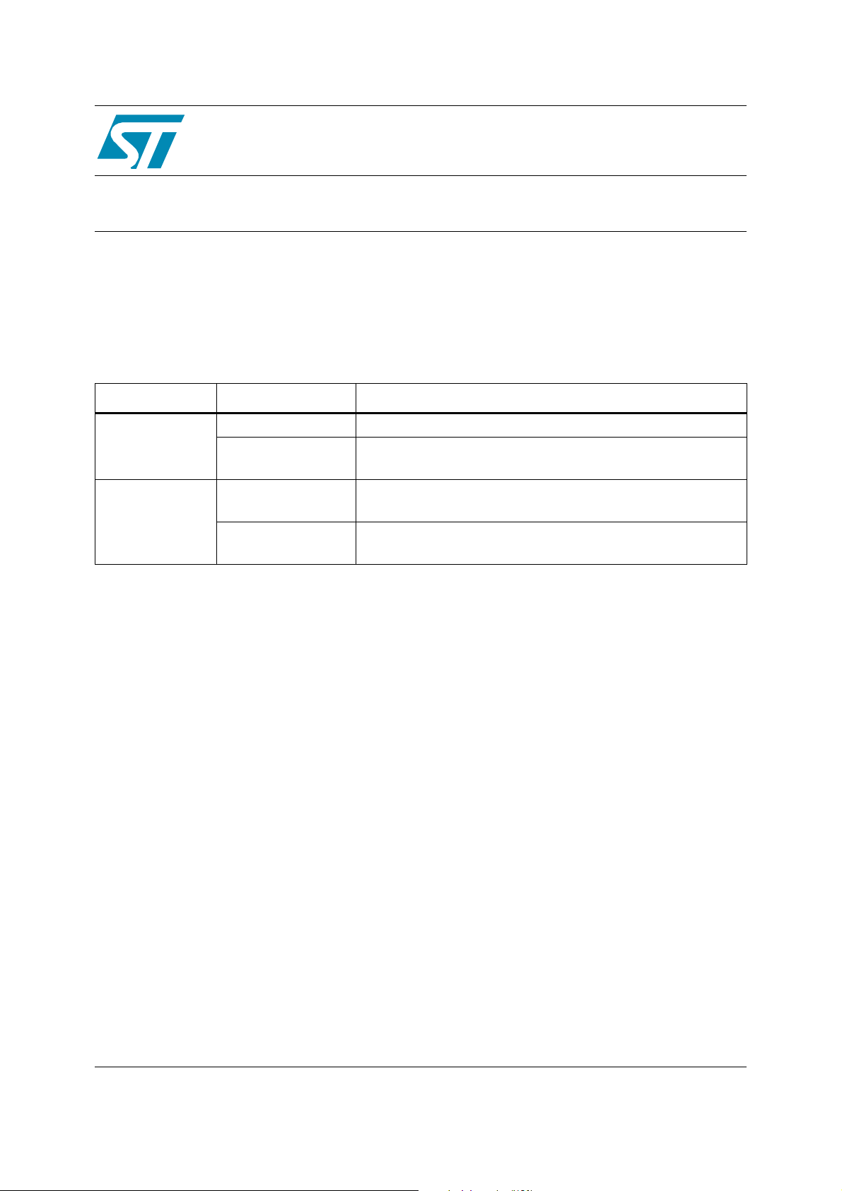
Table 1. Migration cross-reference table
FROM TO Description
ST72F324B 8K to 32K Flash, 32-pin and 44-pin
ST72F324
ST72F325
ST72F321B
ST72F321
ST72F325
16K to 32K Flash, 32-pin and 44-pin
with I²C, Auto Reload Timer and Clock Security System
32K to 60K Flash, 44-pin and 64-pin,
with I²C, Auto Reload Timer
32K to 60K Flash, 44-pin and 64-pin
with I²C, Auto Reload Timer and Clock Security System
Note: Use ST72F325 if your application requires CSS (Clock Security System).
Rev 1
October 2005 1/13
www.st.com
13

AN2187
Contents
1 ST72F324 Migration: feature overview . . . . . . . . . . . . . . . . . . . . . . . . . . . . 3
2 ST72F321 Migration: feature overview . . . . . . . . . . . . . . . . . . . . . . . . . . . . 4
3 Feature compatibility . . . . . . . . . . . . . . . . . . . . . . . . . . . . . . . . . . . . . . . . . . 5
3.1 Pinout . . . . . . . . . . . . . . . . . . . . . . . . . . . . . . . . . . . . . . . . . . . . . . . . . . . . . . . 5
3.2 VDD Rise time . . . . . . . . . . . . . . . . . . . . . . . . . . . . . . . . . . . . . . . . . . . . . . . . 5
3.3 Asynchronous RESET pin . . . . . . . . . . . . . . . . . . . . . . . . . . . . . . . . . . . . . . . 5
3.4 Oscillator pad . . . . . . . . . . . . . . . . . . . . . . . . . . . . . . . . . . . . . . . . . . . . . . . . . 6
3.5 Clock Security System (CSS) . . . . . . . . . . . . . . . . . . . . . . . . . . . . . . . . . . . . . 6
4 Performance improvements . . . . . . . . . . . . . . . . . . . . . . . . . . . . . . . . . . . . . 7
5 New features and peripherals . . . . . . . . . . . . . . . . . . . . . . . . . . . . . . . . . . . 8
5.1 Clock Security System (CSS) . . . . . . . . . . . . . . . . . . . . . . . . . . . . . . . . . . . . . 8
6 Register map . . . . . . . . . . . . . . . . . . . . . . . . . . . . . . . . . . . . . . . . . . . . . . . . . 9
6.1 Register Address . . . . . . . . . . . . . . . . . . . . . . . . . . . . . . . . . . . . . . . . . . . . . . 9
6.2 Register Modifications . . . . . . . . . . . . . . . . . . . . . . . . . . . . . . . . . . . . . . . . . . 10
6.2.1 SICSR Register . . . . . . . . . . . . . . . . . . . . . . . . . . . . . . . . . . . . . . . . . . . . . . . 10
7 Limitations summary . . . . . . . . . . . . . . . . . . . . . . . . . . . . . . . . . . . . . . . . . 11
8 Revision History . . . . . . . . . . . . . . . . . . . . . . . . . . . . . . . . . . . . . . . . . . . . . 12
2/13
AN2187 1 ST72F324 Migration: feature overview
1 ST72F324 Migration: feature overview
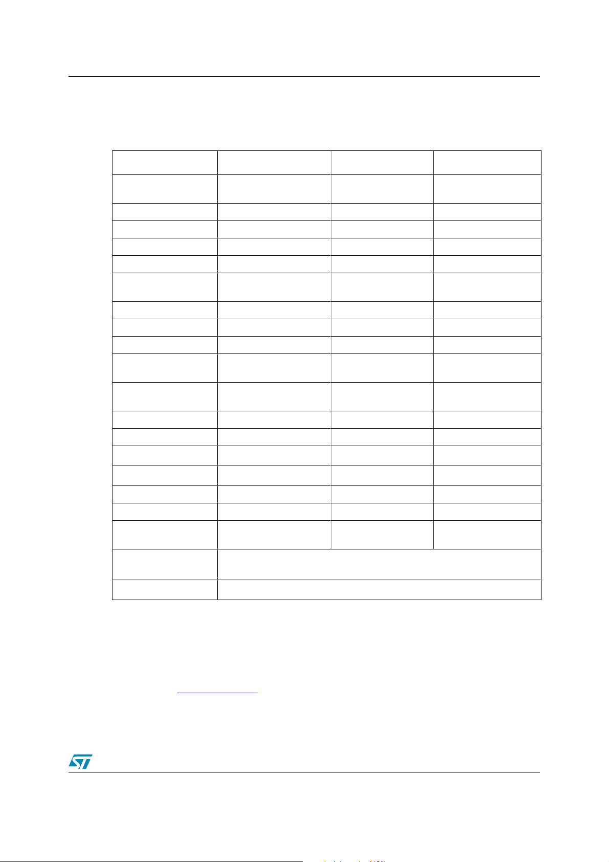
Table 2. ST72F324 migration: feature overview
Feature
1)
ST72F324 ST72F324B ST72F325
Package
Program Memory 8 to 32K Flash - 16 to 32K Flash
Operating Supply 3.8 V to 5.5V - -
Register Map 128 bytes - -
I/Os (High sink) 32/24 pins - -
Power saving Modes
Nested Interrupts Ye s - -
MCC / RTC Ye s - -
Watchdog Ye s - -
16-bit Timer
(OC / IC / PWM)
8-bit PWMART
(OC / IC / PWM)
SPI Ye s - -
SCI Yes - -
2
C
I
ADC Yes (10-bit)
LV D 3 Levels (No change) - -
TQFP44 / SDIP42 /
TQFP32 / SDIP32
Slow / Wait / Active Halt /
Halt
2 Timers (3 / 3 / 2) - -
No -
No - Yes
--
2)
-
3)
-
2)
-
1 Timer
(4 / 0 / 4)
3)
-
CSS No - Yes
ICC mode 39-pulse
Development tools
Programming tools
4)
ST7MDT20x-EMU3 and ST7MTD20-DVP3
ST7MDT20x-EPB and ST7MTD20-DVP3
39-pulse (32k Flash)
36-pulse (8/16k Flash)
ST7232X-SK/RAIS
39-pulse
“-” stands for: No change vs. ST72F324, fully compatible with existing development
Note 1: Refer to the corresponding datasheets for more information.
Note 2: Exit from Active Halt available with external interrupts (see Section 7)
Note 3: improved ADC accuracy
Note 4: Go to http://www.st.com
for information on third-party tools.
3/13
2 ST72F321 Migration: feature overview AN2187
2 ST72F321 Migration: feature overview
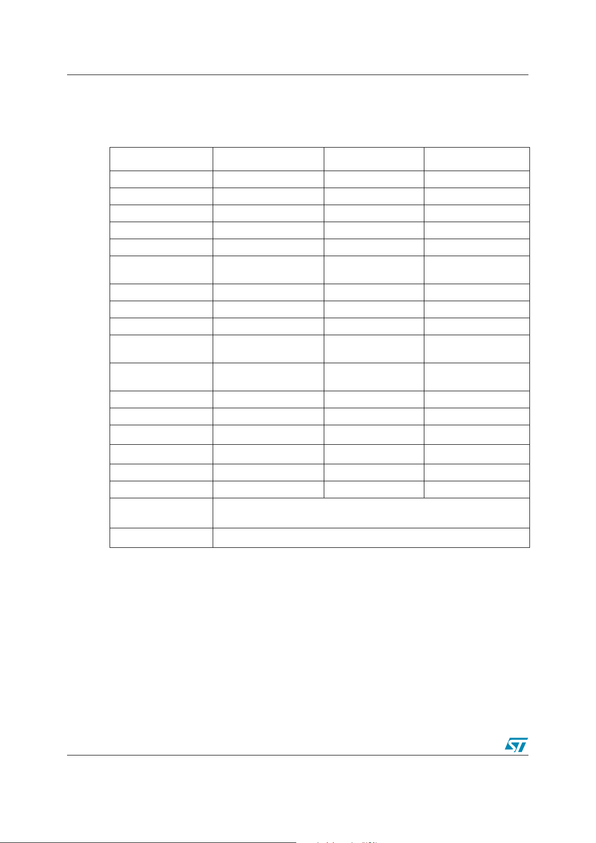
Table 3. ST72F321 Migration: feature overview
Feature
Package TQFP44 / TQFP64 - -
Program Memory 32K to 60KFlash - 16K to 60K Flash
Operating Supply 3.8 V to 5.5V - -
Register Map 128 bytes - -
I/Os (High sink) 48/32 pins - -
Power saving Modes
Nested Interrupts Ye s - -
MCC / RTC Ye s - -
Watchdog Ye s - -
16-bit Timer
(OC / IC / PWM)
8-bit PWMART
(OC / IC / PWM)
1)
ST72F321 ST72F321B ST72F325
Slow / Wait / Active Halt /
Halt
2 Timers (3 / 3 / 2) - -
1 Timer (4 / 0 / 4) - -
2)
-
2)
-
SPI Ye s - -
SCI Yes - -
2
C
I
ADC Yes (10-bit)
LV D 3 Levels - -
CSS No - Yes
Development tools
Programming tools
4)
Ye s - -
3)
-
ST7MDT20x-EMU3 and ST7MTD20-DVP3
ST7232X-SK/RAIS
ST7MDT20x-EPB and ST7MTD20-DVP3
“-” stands for: No change vs. ST72F321, fully compatible with existing development
Note 1: Refer to the corresponding datasheets for more information.
Note 2: Exit from Active Halt available with external interrupts (see Section 7)
Note 3: improved ADC accuracy
Note 4: Go to http://www.st.com for information on third-party tools.
3)
-
4/13

AN2187 3 Feature compatibility
3 Feature compatibility
3.1 Pinout
TQFP44 or TQFP32 pin packages in all salestypes are fully pin to pin compatible. ST72F325
devices have addtional alternate functions for the 8-bit PWMART and I
4).
Table 4. Addition of 8-bit PWMART and I
TQFP44
TQFP32
PWM3
(pin 2)
PWM3
(pin 28)
Note: PWM3-0 are the Pulse Width Modulation outputs and ARTCLK is the external clock for
the 8-bit Auto reload timer. SDAI is the serial data and SCLI is the serial clock pin for the I2C
peripheral. N/A stands for not-available.
3.2 VDD Rise time
Some timing differences exist between the products (see<Blue HT>Table 5). The application
must ensure that the power supply ramps up within the time window specified for the
microcontroller.
Table 5. VDD Rise time
Symbol Description Device Conditions Min Max
Vt
POR
VDD rise time
2
C (see <Blue HT>Table
2
C Alternate Function I/Os
ST72F325 only
PWM2
(pin 3)
N/A N/A
PWM1
(pin 4)
ST72F324 / 324B
ST72F321B / 325
ST72F321 LVD enabled 6µs/V 20ms/V
PWM0
(pin 5)
PWM0
(pin 29)
ARTCLK
(pin 6)
ARTCLK
(pin 30)
LVD enabled 6µs/V 100ms/V
SDAI
(pin 36)
SDAI
(pin 18)
SCLI
(pin 37)
SCLI
(pin 19)
3.3 Asynchronous RESET pin
The VIL/VIH of reset pin has been changed to 0.3Vdd/0.7Vdd from 0.16Vdd/0.85Vdd
respectively (see <Blue HT>Table 6).
Table 6. RESET
VIL 0.16xV
VIH 0.85xV
Pin Characteristics
ST72F324, ST72F321 ST72F324B, ST72F321B, ST72F325
Min Max Min Max
DD
DD
0.3xV
DD
0.7xV
DD
5/13

3 Feature compatibility AN2187
3.4 Oscillator pad
The ST72F324B (32k Flash only), ST72F321B and ST72F325 devices feature a new oscillator
pad which is more tolerant of the crystal type and is not disturbed if the oscillator pins are left
unconnected. When migrating to these, devices the MCU needs to be validated with your
existing resonator / crystal.
Murata 16 MHz 3rd overtone oscillators are not recommended for ST72F324B (32k Flash),
ST72F321B and ST72F325.
For applications requiring a high precision f
4 MHz + PLL. Note that the PLL jitter is improved compared to ST72F324 and ST72F321.
Refer to the Electrical characteristics section of the datasheets.
3.5 Clock Security System (CSS)
CSS has been added in ST72F325 devices. The Clock Security System (CSS) protects the
ST7 against main clock problems. To allow the integration of the security features in the
applications, it is based on a clock filter control and an Internal safe oscillator. The CSS can be
enabled or disabled by option byte.
Please refer to the datasheet for more information.
at 8MHz, the preferred solution is to use
CPU
6/13

AN2187 4 Performance improvements
4 Performance improvements
The ST72F324B, ST72F321B and ST72F325 devices feature many significant improvements
such as:
● Reduced PLL clock jitter
● Lower power consumption
● Improved A/D converter accuracy and negative injection on robust pins.
Refer to the relevant datasheets for more details.
7/13

5 New features and peripherals AN2187
5 New features and peripherals
5.1 Clock Security System (CSS)
CSS has been added in ST72F325 devices. The Clock Security System (CSS) protects the
ST7 against main clock problems. To allow the integration of the security features in the
applications, it is based on a clock filter control and an Internal safe oscillator.
The CSS can be enabled or disabled by an additional option byte:
Option bit 5 (CSS) in option byte 0 is used to enable or disable the CSS. CSS is disabled by
default.
Figure 1. ST72F325 Option Bytes
Default
1
11001
11 1 1 1 0 1 1 1 1
Refer to the relevant datasheets for more details.
8/13

AN2187 6 Register map
6 Register map
Registers are strictly identical between ST72F324 & ST72F324B and between ST72F321 &
ST72F321B.
In the ST72F325, some register addresses and bit locations are added for the CSS and the
extra peripherals available in ST72F325 devices.
Note: For easy software migration, two general rules have to be followed:
● All “reserved” byte memory areas must never be “read” or “write”.
● All “reserved” or “unused” bits must be left unchanged when accessing the byte.
6.1 Register Address
In ST72F325 devices, I2C and 8-bit PWMART are added as new features.
Please, refer to the datasheet for the description of the new features.
Figure 2. Register Map Modifications
ST72F324
@Block
0018h
to
Reserved Area (7 bytes)
001Eh
0073h
to
Reserved Area (7 bytes)
007Dh
Register
Label
ST72F325
@Block
0018h
0019h
001Ah
001Bh
001Ch
001Dh
001Eh
0073h
0074h
0075h
0076h
0077h
0078h
0079h
007Ah
007Bh
007Ch
007Dh
I2C
PWM ART
Register
Label
I2CCRI
I2CSR1
I2CSR2
I2CCCR
I2COAR1
I2COAR2
I2CDR
PWMDCR3
PWMDCR2
PWMDCR1
PWMDCR0
PWMCR
ARTCSR
ARTCAR
ARTARR
ARTICCSR
ARTICR1
ARTICR2
9/13

6 Register map AN2187
6.2 Register Modifications
6.2.1 SICSR Register
Two bits related to CSS have been added in the SICSR (System Integrity Control/Status Register) register.
Figure 3. SICSR Register Changes
SICSR (002Bh)
System Integrity Control/Status Register
70
0 AVDIE AVDF
LVDR
F
000
SICSR (002Bh)
System Integrity Control/Status Register
70
WDG
RF
AVDIEAVDFLVDR
0
F
0 CSSIE CSSD
WDG
RF
10/13

AN2187 7 Limitations summary
7 Limitations summary
Limitations ST72F324 ST72F321 ST72F324B ST72F321B ST72F325
Internal RC Oscillator
Operation
Active Halt wake up by
external interrupt
Negative Injection
current immunity on
Analogic pins
Over frequency on
OSC pad
CSS functionality
Vih(min) / Vil(max)
0.7xVdd / 0.3xVdd
on reset pin
ICC mode entry with
39 pulses
1
2
✔
XX ✔✔✔
XX ✔✔✔
4
X
XX X X ✔
5
X
✔✔ X
✔
2
4
X
5
X
✔✔✔
4
X
✔✔
✔✔✔
6
✔✔
For more details, refer to the KNOWN LIMITATIONS chapter at the end of each datasheet
Note 1: refer to ELECTICAL CHARACTERISTICS chapter of the datasheet
Note 2: no limitation if LVD is enabled.
Note 3: Negative injection current on any of the analog input pins significantly reduces the
accuracy of ADC.
Note 4: When OSC1 or OSC2 is unconnected, main oscillator may overrun above the
maximum frequency guaranteed. The product may then operates in unsafe / undefined state.
Note 5: Vih(min) and Vil(max) on reset pin is 0.85xVdd and 0.16xVdd respectively.
Note 6: ICC 39-pulse is not available for 8/16k Flash devices only
11/13

8 Revision History AN2187
8 Revision History
Date Revision Changes
04-Oct-2005 1 Initial release
12/13

AN2187 8 Revision History
“THE PRESENT NOTE WHICH IS FOR GUIDANCE ONLY AIMS AT PROVIDING CUSTOMERS WITH
INFORMATION REGARDING THEIR PRODUCTS IN ORDER FOR THEM TO SAVE TIME. AS A
RESULT, STMICROELECTRONICS SHALL NOT BE HELD LIABLE FOR ANY DIRECT, INDIRECT OR
CONSEQUENTIAL DAMAGES WITH RESPECT TO ANY CLAIMS ARISING FROM THE CONTENT OF
SUCH A NOTE AND/OR THE USE MADE BY CUSTOMERS OF THE INFORMATION CONTAINED
HEREIN IN CONNECTION WITH THEIR PRODUCTS.”
Information furnished is believed to be accurate and reliable. However, STMicroelectronics assumes no responsibility for the consequences
of use of such information nor for any infringement of patents or other rights of third parties which may result from its use. No license is granted
by implication or otherwise under any patent or patent rights of STMicroelectronics. Specifications mentioned in this publication are subject
to change without notice. This publication supersedes and replaces all information previously supplied. STMicroelectronics products are not
authorized for use as critical components in life support devices or systems without express written approval of STMicroelectronics.
The ST logo is a registered trademark of STMicroelectronics.
All other names are the property of their respective owners
© 2005 STMicroelectronics - All rights reserved
STMicroelectronics group of companies
Australia - Belgium - Brazil - Canada - China - Czech Republic - Finland - France - Germany - Hong Kong - India - Israel - Italy - Japan -
Malaysia - Malta - Morocco - Singapore - Spain - Sweden - Switzerland - United Kingdom - United States of America
www.st.com
13/13
 Loading...