

Page 1

AN2182
Application note
Filters using the ST10 DSP library
Introduction
The ST10F2xx family provides a 16-bit multiply and accumulate unit (MAC) allowing control-oriented
signal processing and filtering widely used in digital applications.
An ST10 DSP software library, developed by STMicroelectronics, contains a set of basic arithmetic
operations such as multiplication as we ll as two main filter functions , FIR (finite impulse response) and IIR
(infinite impulse response), mainly used in digital signal processing.
The first chapter of this application note describes a theoretical digital implementation of four different
filters:
■ Low-pass filter
■ High-pass filter
■ Passband filter
■ Cut-band filter
The method adopted for each filter is th e approximation of the ideal filter model by a FIR filter . This th eory
aims to compute the FIR’s coefficients by truncating the real signal with a known window.
The second chapter illustrates a practical implementation of a low-pass filter using the ST10 DSP library,
its results and its limitations.
July 2007 Rev 1 1/18
www.st.com
18
Page 2

Contents AN2182
Contents
1 ST10 DSP library . . . . . . . . . . . . . . . . . . . . . . . . . . . . . . . . . . . . . . . . . . . . . . 3
2 Digital filtering principles . . . . . . . . . . . . . . . . . . . . . . . . . . . . . . . . . . . . . . . 4
2.1 Fourier transform of a sampled signal . . . . . . . . . . . . . . . . . . . . . . . . . . . . . . 4
2.2 Linear filtering . . . . . . . . . . . . . . . . . . . . . . . . . . . . . . . . . . . . . . . . . . . . . . . . . 4
2.3 Finite impulse response filters . . . . . . . . . . . . . . . . . . . . . . . . . . . . . . . . . . . . 5
3 Low-pass filter . . . . . . . . . . . . . . . . . . . . . . . . . . . . . . . . . . . . . . . . . . . . . . . . 6
4 High-pass filter . . . . . . . . . . . . . . . . . . . . . . . . . . . . . . . . . . . . . . . . . . . . . . . 9
5 Passband filter . . . . . . . . . . . . . . . . . . . . . . . . . . . . . . . . . . . . . . . . . . . . . . . 10
6 Cutoff band filter . . . . . . . . . . . . . . . . . . . . . . . . . . . . . . . . . . . . . . . . . . . . . 11
7 Implementation example using the ST10 DSP library . . . . . . . . . . . . . . . 12
7.1 Overview . . . . . . . . . . . . . . . . . . . . . . . . . . . . . . . . . . . . . . . . . . . . . . . . . . . . 12
7.2 Sampling frequency and FIR coefficients . . . . . . . . . . . . . . . . . . . . . . . . . . . 14
7.3 Results . . . . . . . . . . . . . . . . . . . . . . . . . . . . . . . . . . . . . . . . . . . . . . . . . . . . . 14
7.3.1 Frequency response . . . . . . . . . . . . . . . . . . . . . . . . . . . . . . . . . . . . . . . . . . . 14
7.3.2 Phase response . . . . . . . . . . . . . . . . . . . . . . . . . . . . . . . . . . . . . . . . . . . . . . 15
8 References . . . . . . . . . . . . . . . . . . . . . . . . . . . . . . . . . . . . . . . . . . . . . . . . . . 16
9 Revision history . . . . . . . . . . . . . . . . . . . . . . . . . . . . . . . . . . . . . . . . . . . . . . 17
2/18
Page 3

AN2182 ST10 DSP library
1 ST10 DSP library
The ST10 DSP free library is a set of arithmetic and signal processing functions based on the
ST10 MAC unit. These functions are callable from C and fully compatible with the Tasking
compiler.
This library manipulates signed integers coded on 16 or 32 bits. These integers represent
numbers belonging to the interval [–1, 1[. We name these formats: Q1.31 and Q1.15.
Table 1. Examples of integer representations
–1 -0.5 -0.25 0 0.25 0.5
Q1.15 0xFFFF 0xC000 0xA000 0x0000 0x2000 0x4000 0x7FFF 0x7FFF
Q1.31
0xFFFF
FFFF
0xC000
0000
0xA0000
000
0x00000
000
0x20000
000
0x40000
000
1 - 1/2
0x7FFF
0000
15
0x7FFFFFFF
1 - 1/2
31
For a detailed description of the ST10 DSP libra ry, please refer to the application note AN1442
“Signal processing with ST10-DSP”.
3/18
Page 4
Digital filtering principles AN2182
2 Digital filtering principles
Assume a continuous signal x(t) (the complex form corresponds to the signal’s phase and
magnitude at the instant t) with a pass band B. Assume that this signal will be filtered using a
filter with a continuous impulse response h(t).
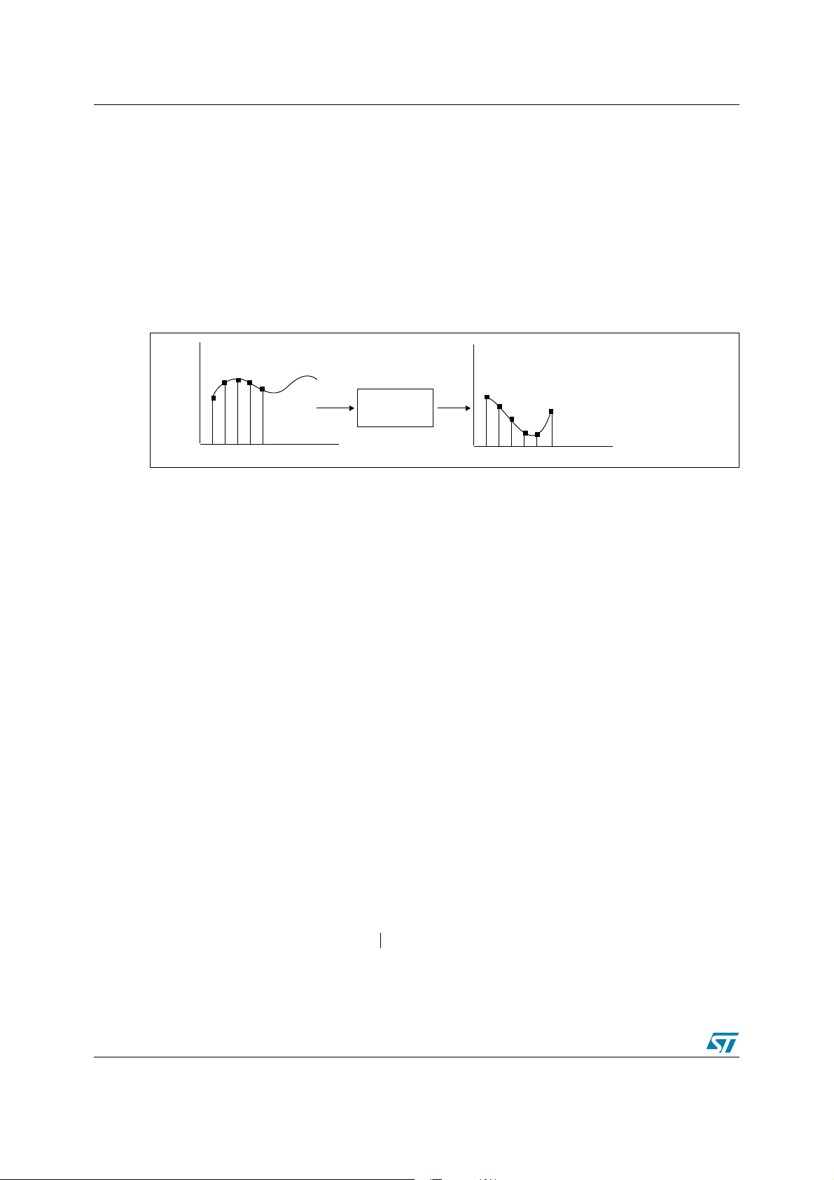
When digital processing has to be used, it is necessary to sample the input signal with a
frequency of F
from the samples obtained at the filter’s output.
Figure 1. Example of input and output signals
Input signal Output signal
The Shannon theorem states that when sampling a signal at discrete intervals, the sampling
frequency F
= 1/Ts (Ts being the sampling period). The output signal is then reconstituted
s
Filter h
should be greater than twice the highest frequency of the input signal.
s
2.1 Fourier transform of a sampled signal
Signals are converted from the time domain to the frequency domain usually through the
Fourier transf orm. With the Fo urier transf orm, the signal is conv erted to a magnitude and pha se
at each frequency.
The Fourier transform of the sampled signal x(k) has the following expression:
∞
Xf() xk()e
=
∑
The time representation can be computed f rom the X(f) as follows:
=
xk() Xf()e
i2kπf
∞–
∞
i– 2kπf
∑
∞–
2.2 Linear filtering
Using the notations defined in the previous section, the output signal y(n) is the convolution of
the input signal x(k) and the filter impulse response h(k) .
yn() hn k–()xk()
∞
==
∑
∞–
hk() xk()⊗()
n
where x(n) = x(nT
4/18
), h(n – k) = h((n – k)Ts) and y(n) = y(nTs).
s
Page 5

AN2182 Digital filtering principles
The output signal frequency response is given by the following expression:
Yf() Hf() Xf()⋅=
where H(f), X(f) and Y(f) are the respective Fourier transforms of h(k), x(k) and y(k).
2.3 Finite impulse response filters
The FIR (Finite Impulse Response) a re non-recu rsiv e filters , mean ing that the outp ut signal y( i)
is a linear combination of N input samples x(k) in the case of a N–1 order filte r. Its equation is
N1–
⎛⎞
yn() akxn k–()
⎜⎟
=
∑
⎜⎟
⎝⎠
k0=
where a
are the FIR’s coefficients.
k
A FIR filter is characterized by its order and its coefficients and can be used to implement any
kinds of filters (low-pass, high-pass, pass-band or cutoff band).
5/18
Page 6
Low-pass filter AN2182
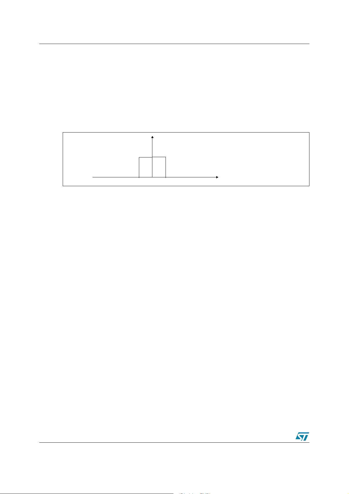
3 Low-pass filter
The aim of this section is to create a low-pass filter with a cutoff frequency Fc and a gain G = 1,
by determining a FIR filter using the digital approach. The FIR coefficien ts correspond to h(n)
where h is its continuous time response and h(n) = h(nT
In the frequency domain, the ideal filter corresponding to these criteria has the following
response:
Figure 2. Ideal low-pass filter frequency response
Magnitude
1
).
s
-F
c
F
0
c
This filter’s impulse response in the time domain is
∞
(1)
ht() Hf()e
∫
This response is sampled with a rate F
2πift
fd
2Fcc2tF
∞–
()sin==
c
= 1/Ts (sampling frequency), so the discrete response
s
has the followi ng expression
∞
( 2)
hst() hnTs()δtnT
=
∑
∞–
The impact of sampling h(t) with a rate F
around F
and a gain of Fs. In fact, the frequency response corresponding to the sampled
s
–()
s
is a periodization of the analog signal spectrum
s
impulse response is
∞
Hsf() FsHf nF
=
Therefore , t o obtain a gain o f 1, t he h
–()
∑
∞–
s
response filter should be divided by Fs. Using equations
s
(1) and (2), the low-pass filter time response becomes:
∞
F
(3)
hst() 2
=
c
------ c 2 n FcT
∑
F
s
∞–
()δtns–()sin
s
Frequency
The impulse response is a sinus cardinal (sinc) function centered at the origin.
6/18
Page 7

AN2182 Low-pass filter
Figure 3. Ideal low-pass filter impulse response
h(kTs)
h(k/2Fc) = 0
h(0)= 2F
k>=1
c
Two issues can be observed at this stage:
First, the filter length is infinite. This means that in order to have the ideal low-pass filter, an
infinite number of filter coefficients is required. In practice, this cannot be done because of the
calculation complexity. To solve this feasibility problem, the filter’s impulse response should be
truncated by a known window. In this application note, we will truncate this response using a
rectangular window.
Truncating the filter’s impulse response, howe ver, changes the ideal rectangular response;
more fluctuations are observed in the pass band. In order to reduce this effect, the FIR’s
coefficients’ numbers can be increased.
Figure 4. Effect of truncating the ideal impulse with a rectangular window
W(n)
Magnitude
1
Time domain
Time
-F
c
Frequency domain
F
0
c
Frequency
In the following sections, we will note:
● W is the window’s time response
● N the number of coefficients included in the window W. This means that the window’s
length is (N–1)T
. The window should be large enough to include at least the first lobe of
s
the sinus cardinal.
Second, the truncated response is finite but not causal because there are non-null coefficients
on the negative time axis. This means that the filter reacts before being excit ed by the input
signal. Practically, this filter is not feasible. To solve this issue, we will shift the filter’s impulse
response by (N–1)T
/2. By doing so , all coefficients on the negativ e time axis are 0 and the filter
s
becomes feasible.
f
⋅⋅
-----F
s
The impact of shifting the filter’s time response is a phase shift of in the
N1–()π
frequency domain.
7/18
Page 8

Low-pass filter AN2182
By fixing a number of points N and a sampling period Ts, the FIR coefficients h(n)
corresponding to a low-pass filter with a cutoff frequency F
F
hn() 2
(4)
c
⎛⎞
------ c 2Fcn
⎝⎠
F
s
N1–
⎛⎞
–
⎝⎠
------------2
T
Wn
⋅sin=
s
N1–
⎛⎞
–
-------------
⎝⎠
2
c
are
if n = 0 .. N – 1 and 0 if n > N – 1.
8/18
Page 9

AN2182 High-pass filter
4 High-pass filter
The aim of this section is to create a high-pass filter with a cutoff frequency Fc and a gain G = 1,
by determining a FIR h filter using the digital approach. The FIR coe fficients corr espond to h(n)
where h is its continuous time response and h(n) = h(nT
In the frequency domain, the ideal high-pass filter corresponding to these criteria has the
following response:
Figure 5. Ideal high-pass filter frequency response
1
).
s
1
-F
s
If we consider H
and H
(f) the frequency response of the low- pass filter with a cutoff fr equency Fc, we can easily
L
-F
F
-F
0
c
High-pass filter F
Low-pass filter F
(f) the frequency response of the high-pass filter with a cutoff frequency Fc
H
F
c
s
c
c
-F
s
c
F
0
F
c
s
notice that
(5)
HHf() 1HLf()–=
In the time domain, this gives
hHn() δn
(6)
⎛⎞
N1–
⎛⎞
–
-------------
⎜⎟
⎝⎠
⎝⎠
2
F
c
2
⎛⎞
sin–
------ c 2Fcn
⎝⎠
F
s
N1–
⎛⎞
–
-------------
⎝⎠
2
⋅=
T
s
N1–
⎛⎞
Wn
–
-------------
⎝⎠
2
where N is the number of the filter’s coefficients, N–1 is the filter’s order and W is the window’s
time function.
In the case of a high-pass filter, N should be odd because of the dirac.
9/18
Page 10

Passband filter AN2182
5 Passband filter
The aim of this section is to create a passband filter with a pass frequency F1, a cutoff
frequency F2> F1, and a gain G=1, by determining a FIR h filter usin g the digital approach.
In the frequency domain, the ideal passband filter corresponding to these criteria has the
following response:
Figure 6. Ideal passband filter frequency response
Magnitude
1
-F2
-F1
F10
F2
Frequency
This filter’s impulse response in the time domain is
∞
ht() Hf()e
∫
∞–
2πift
F1–
fd
2πift
e
∫
F2–
F2
2πift
fd
e
+2F
∫
F1
fd
2
c2F2t()2F1c2F1t()sin–sin== =
Here, the same method described in the section entitled Lo w-pass filter is handled. Please ref er
to this section for more details.
If we fix N the number of the filter’s coefficients and T
(7)
hn() 2
F
⎛⎞
2
⎛⎞
sin 2
------ -c2F2n
⎜⎟
⎝⎠
⎝⎠
F
s
N1–
⎛⎞
–
-------------
⎝⎠
2
T
s
F
1
⎛⎞
sin–
------ -c2F1n
⎝⎠
F
s
the sampling period then we obtain
s
N1–
⎛⎞
–
-------------
⎝⎠
2
⋅=
T
s
N1–
⎛⎞
Wn
–
-------------
⎝⎠
2
with n = 0.. N – 1 and where
● N is the number of the FIR coefficients
● N – 1 is the FIR’s order
● W is the window time response
10/18
Page 11

AN2182 Cutoff band filter
6 Cutoff band filter
The aim of this section is to create a cutoff band filter with a cutoff frequency F1, a pass
frequency F2> F1, and a gain of G=1, by determining a FIR filter using the digital approach.
The FIR coefficients correspond to h(n) where h is the contin uous time response of the filter
and h(n) = h(nT
In the frequency domain, the ideal cutoff band filter corresponding to these criteria has the
following response:
Figure 7. Ideal cut-band filter frequency response
).
s
Magnitude
1
0
-F2
-F1
Cut-band filter
Passband filter
F1
If we consider
● H
(f) the frequency response of the passband filter with a pass frequency F1 and cutoff
P
frequency F2
● H
(f) the frequency response of the cutoff band filter with a cutoff frequency F1 and pass
C
frequency F2
● T
is the sampling period
s
then, we can easily notice that
(8)
HCf() 1HPf()–=
In the time domain, this gives
F
⎛⎞
hCn() δn
⎛⎞
⎝⎠
–
N1–
------------2
2
2
------ -c2F2n
sin 2
–=
⎜⎟
F
⎝⎠
s
F2
Frequency
N1–
⎛⎞
⎛⎞
⎝⎠
–
⎝⎠
------------2
T
s
-F2
F
1
⎛⎞
------ -c2F1n
sin–
⎝⎠
F
s
Magnitude
1
–
N1–
------------2
F10
T
s
-F1
⎛⎞
⎝⎠
F2
Frequency
with n = 0.. N – 1 and where
● N is the number of FIR coefficients
● N – 1 is the FIR’s order
● W is the window time response
In the case of a cutoff band filter, N should be odd because of the dirac, that is the FIR’s order
should be even.
11/18
Page 12

Implementation example using the ST10 DSP library AN2182
7 Implementation example using the ST10 DSP library
7.1 Overview
In this example , an input signal is fed to an analog input of the ST10F27x, processed by a
digital low-pass filter and then output on a PWM output setup as a digital to analog converter.
The digital filter is a low-pass filter with a cutoff frequency equal to 2 kHz and an order of 14
implemented on the ST10F27x using the DSP library provided by STMicroelectronics.
Figure 8. Low-pass filter modules
P5.0
Input signal
P5.0
ADC
module
Signal
sampled
Lowpass
filter
DSP
ST10F276
Signal
filtered
PWM
module
P7.0
27 kΩ
220pc
The whole implementation includes the following elements:
● ADC (analog-to-digital converter): the 10-bit ADC of the ST10F27x is used. The input
signal is entered on channel 0 (P5.0) of the ST10F27x. The ADC conversion time is
4.85 µs (ADCST = ADCTC and ST10 frequency = 40 MHz). When the conversion is
complete, the result stored in the ADDAT register is provided to the FIR filter module.
● Digital filter module: it provides a digital filtered sample. The function used in this
application is the fir_q15_q15_q15() provided in the LibST10.h. This means that the
inputs, outputs and the FIR coeffi cients are fractional between –1 and 1 and are coded in
the format Q1.15.
● DAC (digital-to-analog converter): this module converts the digital filtered signal into an
analog one. An 8-bit DAC is implemented using the ST10F27x PWM and an analog lowpass filter RC. The PWM frequency is 158.8 kHz. The RC filter is used to retain the
continuous components and to remov e the freq uency of the PWM module . In our case , the
RC cutoff frequency is 26.8 kHz. The digital filtered sample sets the pulse width of the
PWM signal.
Output signal
12/18
Page 13

AN2182 Implementation example using the ST10 DSP libra ry
The following flowchart summarizes the software implementation of the low-pass filter:
Figure 9. Low-pass filter flowchart
PWM initialization (PP0 = 0xFF)
FIR structure initialization
ADC initialization
Circular buffer initialization
(1)
(2)
A
PWMIR = 1
No
Yes
Clear PWMIR
Trigger ADC conversion
ADCIR = 1
No
Yes
ADCIR = 0
Update the circular buffer with (ADDAT << 5)
Apply the filter->Output
(3)
PW0 = PP0 +1 - (Output >> 7)
(4)
B
1. Please refer to the technical note ST10 DSP library for a detailed description of the FIR structure used and its
fields.
2. If the filter’s order is 14, 15 input samples are needed to compute an output. A circular buffer is used to store
the 15 input samples of the input signal. The size of the circular buffer is 2 x (filter’s order +1), which is 30 in this
example. An input sample is stored twice in the circular buffer: at buffer[i] and buffer[i + filter’s order +1] where
0<= i<= filter’s order.
3. The ST10F27x ADC converts analog voltages between 0 and 5V into 10-bit digital values. The inputs for the
fir_q15_q15_q15 should be fractional. To normalize these samples, they are shifted to the left.
4. The FIR function delivers a fractional output coded on 16 bits(Q1.15). The DAC realized with the ST10F27x is
an 8-bit one.
13/18
Page 14

Implementation example using the ST10 DSP library AN2182
7.2 Sampling frequency and FIR coefficients
Using the flowchart in the previous section, the samplin g period is the time needed between
point A and point B.
To calculate the FIR’s coefficients , the sa mpling period should be kno wn. W e mea sure the ti me
between points A and B and the result is 17.5 kHz.
Note that to reconstitute the filtered signal, the input signal should not contain frequencies
greater than 8.75 kHz.
The FIR’s coefficients are then computed according to this sampling frequency
h0()
h1()
h2()
h3()
h4()
h5()
h6()
h7()
h8()
h9()
h10()
h11()
h12()
h13()
h14()
0.23 c 1.61–()sin
0.23 c 1.37–()sin
0.23 c 1.14–()sin
0.23 c 0.914–()sin
0.23 c 0.68–()sin
0.23 c 0.46–()sin
0.23 c 0.23–()sin
0.23 c 0()sin
0.23 c 0.23()sin
0.23 c 0.46()sin
0.23 c 0.68()sin
0.23 c 0.914()sin
0.23 c 1.14()sin
0.23 c 1.37()sin
0.23 c 1.61()sin
0.0428–
0.049–
0.0273–
0.0214
0.0902
0.1579
0.2105
0.23
0.2105
0.1579
0.0902
0.0214
0.0273–
0.049–
0.0428–
7.3 Results
To analyze the filter’s f requency and phase responses, a sinusoidal signal of a 2V amplitude is
used. The input voltage varies between 0 and 2 V.
7.3.1 Frequency response
To draw the filter’s frequency response, th e amplitude of the output signal is measured.
···
1402–
1605–
895–
701
2956
5174
6898
7537
6898
5174
2956
701
895–
1605–
1402–
15–
2
⋅===
The following figure gives the filter’s response.
Figure 10. Filter’s frequency response
10
0
1 10 100 1000 10000
-10
Gain in dB
-20
-30
14/18
Frequency
Page 15

AN2182 Implementation example using the ST10 DSP libra ry
7.3.2 Phase response
The following figure gives the phase response.
Figure 11. Phase response
120
20
1 10 100 1000 10000
Phase in °
-80
-180
Frequency
The code implemented to generate this digital low-pass filter can be used to implement a highpass, a passband or a cut off band filter. One simply needs to change the filter’ s coefficients and
the number of coefficients. However, with this implementation, care should be taken with the
sampling frequency, which changes with the filter’s coefficients number and the ST10F27x
frequency.
15/18
Page 16

References AN2182
8 References
1. ST10F276 user manual
2. ST10F276 datasheet
3. AN1442 Signal processing with ST10-DSP, application note
16/18
Page 17

AN2182 Revision history
9 Revision history
Table 2. Document revision history
Date Revision Changes
19-Jul-2007 1 Initial release.
17/18
Page 18

AN2182
Please Read Carefully:
Information in this document is provided solely in connection with ST products. STMicroelectronics NV and its subsidiaries (“ST”) reserve the
right to make changes, corrections, modifications or improvements, to this document, and the products and services described herein at any
time, without notice.
All ST products are sold pursuant to ST’s terms and conditions of sal e.
Purchasers are solely res ponsibl e fo r the c hoic e, se lecti on an d use o f the S T prod ucts and s ervi ces d escr ibed he rein , and ST as sumes no
liability whatsoever relati ng to the choice, selection or use of the ST products and services de scribed herein.
No license, express or implied, by estoppel or otherwise, to any intellectual property rights is granted under this document. If any part of this
document refers to any third pa rty p ro duc ts or se rv ices it sh all n ot be deem ed a lice ns e gr ant by ST fo r t he use of su ch thi r d party products
or services, or any intellectua l property c ontained the rein or consi dered as a warr anty coverin g the use in any manner whats oever of suc h
third party products or servi ces or any intellectual property contained therein.
UNLESS OTHERWISE SET FORTH IN ST’S TERMS AND CONDITIONS OF SALE ST DISCLAIMS ANY EXPRESS OR IMPLIED
WARRANTY WITH RESPECT TO THE USE AND/OR SALE OF ST PRODUCTS INCLUDING WITHOUT LIMITATION IMPLIED
WARRANTIES OF MERCHANTABILITY, FITNESS FOR A PARTICUL AR PURPOS E (AND THEIR EQUIVALE NTS UNDER THE LAWS
OF ANY JURISDICTION), OR INFRINGEMENT OF ANY PATENT, COPYRIGHT OR OTHER INTELLECTUAL PROPERTY RIGHT.
UNLESS EXPRESSLY APPROVED IN WRITING BY AN AUTHORIZED ST REPRESENTATIVE, ST PRODUCTS ARE NOT
RECOMMENDED, AUTHORIZED OR WARRANTED FOR USE IN MILITARY, AIR CRAFT, SPACE, LIFE SAVING, OR LIFE SUSTAINING
APPLICATIONS, NOR IN PRODUCTS OR SYSTEMS WHERE FAILURE OR MALFUNCTION MAY RESULT IN PERSONAL INJ URY,
DEATH, OR SEVERE PROPERTY OR ENVIRONMENTAL DAMAGE. ST PRODUCTS WHICH ARE NOT SPECIFIED AS "AUTOMOTIVE
GRADE" MAY ONLY BE USED IN AUTOMOTIVE APPLICATIONS AT USER’S OWN RISK.
Resale of ST products with provisions different from the statements and/or technical features set forth in this document shall immediately void
any warranty granted by ST fo r the ST pro duct or serv ice describe d herein and shall not cr eate or exten d in any manne r whatsoever , any
liability of ST.
ST and the ST logo are trademarks or registered trademarks of ST in various countries.
Information in this document su persedes and replaces all info rmation previously supplied .
The ST logo is a registered trademark of STMicroelectronics. All other names are the property of their respective owners.
© 2007 STMicroelectronics - All rights reserved
STMicroelectronics group of compan ie s
Australia - Belgium - Brazil - Canada - China - Czech Republic - Finland - France - Germany - Hong Kong - India - Israel - Italy - Japan -
Malaysia - Malta - Morocco - Singapore - Spain - Sweden - Switzerland - United Kingdom - United States of America
www.st.com
18/18
 Loading...