

Page 1

AN2169
Application note
Porting an application
from the ST10F168 to the ST10F276
Introduction
The ST10F276 is a new derivative of the STMicroelectronics ST10 family of 16-bit single-chip CMOS
microcontrollers. This document aims to describe the differences between the ST10F168 and ST10F276
and is intended for hardware or software designers who are adapting existing applications based on the
ST10F168 to the ST10F276.
This document will present the modified functionalities of the ST10F276, then the new ones before
looking at the modified and new registers. For each part, the differences with the ST10F168 that have an
impact will be shown and some advice on the way they can be handled will be given.
July 2006 Rev 1 1/33
www.st.com
33
Page 2

AN2169
Contents
1 Modified features . . . . . . . . . . . . . . . . . . . . . . . . . . . . . . . . . . . . . . . . . . . . . . 5
1.1 Pin-out . . . . . . . . . . . . . . . . . . . . . . . . . . . . . . . . . . . . . . . . . . . . . . . . . . . . . . . 5
1.1.1 Pin-out modification summary . . . . . . . . . . . . . . . . . . . . . . . . . . . . . . . . . . . . . 5
1.1.2 Pin 99 . . . . . . . . . . . . . . . . . . . . . . . . . . . . . . . . . . . . . . . . . . . . . . . . . . . . . . . 6
1.1.3 Pins 143 & 144 . . . . . . . . . . . . . . . . . . . . . . . . . . . . . . . . . . . . . . . . . . . . . . . . 6
1.1.4 Pin 84 . . . . . . . . . . . . . . . . . . . . . . . . . . . . . . . . . . . . . . . . . . . . . . . . . . . . . . . 6
1.1.5 Pin 56 . . . . . . . . . . . . . . . . . . . . . . . . . . . . . . . . . . . . . . . . . . . . . . . . . . . . . . . 7
1.2 Maximum CPU frequency . . . . . . . . . . . . . . . . . . . . . . . . . . . . . . . . . . . . . . . . 7
1.2.1 Hardware impact . . . . . . . . . . . . . . . . . . . . . . . . . . . . . . . . . . . . . . . . . . . . . . . 7
1.2.2 software impact . . . . . . . . . . . . . . . . . . . . . . . . . . . . . . . . . . . . . . . . . . . . . . . . 7
1.3 XRAM . . . . . . . . . . . . . . . . . . . . . . . . . . . . . . . . . . . . . . . . . . . . . . . . . . . . . . . 7
1.3.1 Hardware impact . . . . . . . . . . . . . . . . . . . . . . . . . . . . . . . . . . . . . . . . . . . . . . . 7
1.3.2 Software impact . . . . . . . . . . . . . . . . . . . . . . . . . . . . . . . . . . . . . . . . . . . . . . . . 7
1.4 Flash memory . . . . . . . . . . . . . . . . . . . . . . . . . . . . . . . . . . . . . . . . . . . . . . . . . 8
1.4.1 Hardware impact . . . . . . . . . . . . . . . . . . . . . . . . . . . . . . . . . . . . . . . . . . . . . . . 9
1.4.2 Software impact . . . . . . . . . . . . . . . . . . . . . . . . . . . . . . . . . . . . . . . . . . . . . . . . 9
1.5 A/D converter . . . . . . . . . . . . . . . . . . . . . . . . . . . . . . . . . . . . . . . . . . . . . . . . 10
1.5.1 Hardware / Software impact: conversion timing control . . . . . . . . . . . . . . . . . 10
1.5.2 Hardware impact . . . . . . . . . . . . . . . . . . . . . . . . . . . . . . . . . . . . . . . . . . . . . . 10
1.5.3 Software impact . . . . . . . . . . . . . . . . . . . . . . . . . . . . . . . . . . . . . . . . . . . . . . . 11
1.6 PLL and on-chip main oscillator . . . . . . . . . . . . . . . . . . . . . . . . . . . . . . . . . . 12
2 New functionalities . . . . . . . . . . . . . . . . . . . . . . . . . . . . . . . . . . . . . . . . . . . 14
2.1 CAN module . . . . . . . . . . . . . . . . . . . . . . . . . . . . . . . . . . . . . . . . . . . . . . . . . 14
2.1.1 Hardware impact . . . . . . . . . . . . . . . . . . . . . . . . . . . . . . . . . . . . . . . . . . . . . . 14
2.1.2 Software impact . . . . . . . . . . . . . . . . . . . . . . . . . . . . . . . . . . . . . . . . . . . . . . . 14
2.2 Real time clock . . . . . . . . . . . . . . . . . . . . . . . . . . . . . . . . . . . . . . . . . . . . . . . 14
2.2.1 Hardware impact . . . . . . . . . . . . . . . . . . . . . . . . . . . . . . . . . . . . . . . . . . . . . . 14
2.2.2 Software impact . . . . . . . . . . . . . . . . . . . . . . . . . . . . . . . . . . . . . . . . . . . . . . . 14
2.3 MAC unit . . . . . . . . . . . . . . . . . . . . . . . . . . . . . . . . . . . . . . . . . . . . . . . . . . . . 14
2.3.1 Hardware impact . . . . . . . . . . . . . . . . . . . . . . . . . . . . . . . . . . . . . . . . . . . . . . 14
2.3.2 Software impact . . . . . . . . . . . . . . . . . . . . . . . . . . . . . . . . . . . . . . . . . . . . . . . 14
2.4 Additional X-peripherals . . . . . . . . . . . . . . . . . . . . . . . . . . . . . . . . . . . . . . . . 15
2/33
Page 3

AN2169
2.4.1 Hardware impact . . . . . . . . . . . . . . . . . . . . . . . . . . . . . . . . . . . . . . . . . . . . . . 15
2.4.2 Software impact . . . . . . . . . . . . . . . . . . . . . . . . . . . . . . . . . . . . . . . . . . . . . . . 15
2.5 New multiplexer for X-interrupts . . . . . . . . . . . . . . . . . . . . . . . . . . . . . . . . . . 15
2.5.1 Hardware impact . . . . . . . . . . . . . . . . . . . . . . . . . . . . . . . . . . . . . . . . . . . . . . 16
2.5.2 Software impact . . . . . . . . . . . . . . . . . . . . . . . . . . . . . . . . . . . . . . . . . . . . . . . 16
2.6 Programmable divider on CLKOUT . . . . . . . . . . . . . . . . . . . . . . . . . . . . . . . 17
2.6.1 Hardware impact . . . . . . . . . . . . . . . . . . . . . . . . . . . . . . . . . . . . . . . . . . . . . . 18
2.6.2 Software impact . . . . . . . . . . . . . . . . . . . . . . . . . . . . . . . . . . . . . . . . . . . . . . . 18
3 Modified registers . . . . . . . . . . . . . . . . . . . . . . . . . . . . . . . . . . . . . . . . . . . . 19
3.1 WDTCON register . . . . . . . . . . . . . . . . . . . . . . . . . . . . . . . . . . . . . . . . . . . . . 19
3.1.1 Hardware impact . . . . . . . . . . . . . . . . . . . . . . . . . . . . . . . . . . . . . . . . . . . . . . 20
3.1.2 Software impact . . . . . . . . . . . . . . . . . . . . . . . . . . . . . . . . . . . . . . . . . . . . . . . 20
3.2 PICON register . . . . . . . . . . . . . . . . . . . . . . . . . . . . . . . . . . . . . . . . . . . . . . . 20
3.2.1 Hardware impact . . . . . . . . . . . . . . . . . . . . . . . . . . . . . . . . . . . . . . . . . . . . . . 21
3.2.2 Software impact . . . . . . . . . . . . . . . . . . . . . . . . . . . . . . . . . . . . . . . . . . . . . . . 21
3.3 IDCHIP register . . . . . . . . . . . . . . . . . . . . . . . . . . . . . . . . . . . . . . . . . . . . . . . 21
3.3.1 Hardware Impact . . . . . . . . . . . . . . . . . . . . . . . . . . . . . . . . . . . . . . . . . . . . . . 22
3.3.2 Software Impact . . . . . . . . . . . . . . . . . . . . . . . . . . . . . . . . . . . . . . . . . . . . . . . 22
4 New registers . . . . . . . . . . . . . . . . . . . . . . . . . . . . . . . . . . . . . . . . . . . . . . . . 23
4.1 XPERCON register . . . . . . . . . . . . . . . . . . . . . . . . . . . . . . . . . . . . . . . . . . . . 23
4.1.1 Hardware impact . . . . . . . . . . . . . . . . . . . . . . . . . . . . . . . . . . . . . . . . . . . . . . 24
4.1.2 Software impact . . . . . . . . . . . . . . . . . . . . . . . . . . . . . . . . . . . . . . . . . . . . . . . 24
4.2 XPEREMU register . . . . . . . . . . . . . . . . . . . . . . . . . . . . . . . . . . . . . . . . . . . . 24
4.2.1 Hardware Impact . . . . . . . . . . . . . . . . . . . . . . . . . . . . . . . . . . . . . . . . . . . . . . 24
4.2.2 Software Impact . . . . . . . . . . . . . . . . . . . . . . . . . . . . . . . . . . . . . . . . . . . . . . . 25
4.3 EXISEL register . . . . . . . . . . . . . . . . . . . . . . . . . . . . . . . . . . . . . . . . . . . . . . 25
4.4 Additional Ports Input Control: XPICON register . . . . . . . . . . . . . . . . . . . . . 26
4.4.1 Hardware impact . . . . . . . . . . . . . . . . . . . . . . . . . . . . . . . . . . . . . . . . . . . . . . 26
4.4.2 Software impact . . . . . . . . . . . . . . . . . . . . . . . . . . . . . . . . . . . . . . . . . . . . . . . 26
4.5 XMISC register . . . . . . . . . . . . . . . . . . . . . . . . . . . . . . . . . . . . . . . . . . . . . . . 27
4.5.1 Hardware impact . . . . . . . . . . . . . . . . . . . . . . . . . . . . . . . . . . . . . . . . . . . . . . 27
4.5.2 Software impact . . . . . . . . . . . . . . . . . . . . . . . . . . . . . . . . . . . . . . . . . . . . . . . 27
4.6 Emulation dedicated registers . . . . . . . . . . . . . . . . . . . . . . . . . . . . . . . . . . . . 27
4.6.1 Hardware impact . . . . . . . . . . . . . . . . . . . . . . . . . . . . . . . . . . . . . . . . . . . . . . 28
3/33
Page 4

AN2169
4.6.2 Software impact . . . . . . . . . . . . . . . . . . . . . . . . . . . . . . . . . . . . . . . . . . . . . . . 28
5 Electrical characteristics . . . . . . . . . . . . . . . . . . . . . . . . . . . . . . . . . . . . . . 29
5.1 DC characteristics . . . . . . . . . . . . . . . . . . . . . . . . . . . . . . . . . . . . . . . . . . . . . 29
5.1.1 Absolute maximum ratings . . . . . . . . . . . . . . . . . . . . . . . . . . . . . . . . . . . . . . 29
5.1.2 DC characteristics . . . . . . . . . . . . . . . . . . . . . . . . . . . . . . . . . . . . . . . . . . . . . 29
6 References . . . . . . . . . . . . . . . . . . . . . . . . . . . . . . . . . . . . . . . . . . . . . . . . . . 31
7 Revision history . . . . . . . . . . . . . . . . . . . . . . . . . . . . . . . . . . . . . . . . . . . . . . 32
4/33
Page 5
AN2169 Modified features
1 Modified features
1.1 Pin-out
1.1.1 Pin-out modification summary
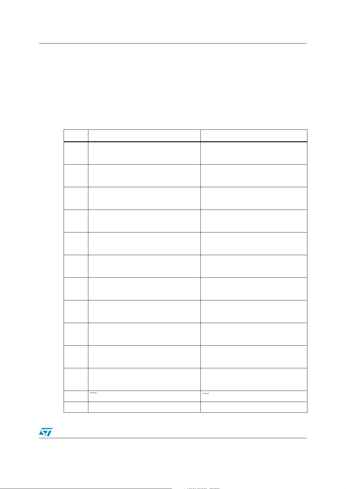
Ta bl e 1 below summarizes the modifications made in the pin-out.
Table 1. Pin-out modification summary
Pin no. ST10F276 pin function ST10F168 pin function
6 (P6.5)
7 (P6.6)
8 (P6.7)
9 (P8.0)
12
(P8.3)
15(P8.6)
16(P8.7)
89
(P4.4)
HOLD External Master Hold request Input
SCLK1 SSC1 Master Clock Output
SCLK1 SSC1 Slave Clock Input
HLDA Hold Acknowledge Output
MTSR1 SS1 Master Transmit
MTSR1 SS1 Slave Receive O/I
BREQ Bus Request Output
MRST1 SSC1 Master receive
MRST1 SSC1 Slave Transmit I/O
CC16IO: CAPCOM2 CC16 Capture-In
CC16IO: CAPCOM2 CC16 Compare-Out
XPWM0: PWM1 Channel0 Output
CC19IO: CAPCOM2 CC19 Capture-In
CC19IO: CAPCOM2 CC19 Compare-Out
XPWM3: PWM1Channel3 Output
CC22IO: CAPCOM2 CC22 Capture-In
CC22IO: CAPCOM2 CC22 Compare-Out
RXD1: ASC1 Data Input(Asynch) or I/O(Synch)
CC23IO: CAPCOM2 CC23 Capture-In
CC23IO: CAPCOM2 CC23 Compare-Out
TXD1: ASC1Clock/Data output(Asyn/Syn)
A20 segment address line
CAN2_RxD CAN2 Receive Data Input
SCL I2C Interface Serial Clock
HOLD External Master Hold request Input
HLDA Hold Acknowledge Output
BREQ Bus Request Output
CC16IO: CAPCOM2 CC16 Capture-In
CC16IO: CAPCOM2 CC16 Compare-Out
CC19IO: CAPCOM2 CC19 Capture-In
CC19IO: CAPCOM2 CC19 Compare-Out
CC22IO: CAPCOM2 CC22 Capture-In
CC22IO: CAPCOM2 CC22 Compare-Out
CC23IO: CAPCOM2 CC23 Capture-In
CC23IO: CAPCOM2 CC23 Compare-Out
A20 segment address line
90
(P4.5)
91(P4.6)
92
(P4.7)
99
143 XTAL3
A21 segment address line
CAN1_RxD CAN1 Receive Data Input
CAN2_RXD CAN2 Receive Data Input
A22 segment address line
CAN1_TxD CAN1 TransmitData Output
CAN2_TXD CAN2 TransmitData Output
A23 segment address line
CAN2_TxD CAN2 TransmitData Output
SDA I2C Interface Serial Data
& V
EA
STBY
5/33
A21 segment address line
CAN_RxD CAN Receive Data Input
A22 segment address line
CAN_TxD CAN TransmitData Output
A23 segment address line
EA
V
ss
Page 6

Modified features AN2169
Pin no. ST10F276 pin function ST10F168 pin function
V
144 XTAL4
84 RPD Vpp / RPD
56 V18 1.8v decoupling pin
Digital supply voltage
DD
V
digital supply voltage
DD
1.1.2 Pin 99
On the ST10F168, pin 99 is EA and used upon reset to select the start from internal flash or
external memory.
Now, on the ST10F276, it has an the additional function of providing the 5V power supply to the
device in standby mode (new power saving mode) and is therefore named EA
Hardware impact
For an application not using the Stand by mode, no change is required on the PCB. However,
for the application to use it , the EA
- V
pin must be separated from the common 5v and
STBY
have a specific supply path.
Software impact
- V
STBY
.
None.
1.1.3 Pins 143 & 144
These pins were a Vss-VDD pair in the ST10F168. Now, on the ST10F276, they are used as
XTAL3-XTAL4 pair for connection to an optional 32Khz crystal to clock the device during powerdown.
Hardware impact
PCB must be redesigned. In case the optional 32Khz is not used, XTAL3 must be linked to
ground as it was in the ST10F168 but XTAL4 shall be left open.
Software impact
In case the optional 32Khz is not used, the bit OFF32 of the RTCCON register shall be set.
Prior to setting the OFF32 bit in RTCCON register, the RTC must be enabled by setting
RTCEN, bit 4 of XPERCON, and XPEN, bit3 of SYSCON.
1.1.4 Pin 84
This pin was named Vpp/RPD on the ST10F168 and was the 12v input pin Flash programming.
In the ST10F276, it is now only used as RPD.
Hardware impact
This pin is no longer designed to accept 12V inputs. Its ratings are the same as any other pin: -
0.5V to V
+ 0.5V.
DD
Software impact
None.
6/33
Page 7
AN2169 Modified features
1.1.5 Pin 56
For the ST10F168, this is VDD pin connected to 5Volts.
For the ST10F276, it is a 1.8V decoupling pin and named V18. A decoupling capacitor must be
connected between this pin and the nearest V
ss
pin.
Hardware impact
The application board should be re-designed in order to introduce the decoupling capacitor.
Software impact
None
1.2 Maximum CPU frequency
ST10F168 ST10F276
Maximum CPU Frequency (MHz) 25 64
1.2.1 Hardware impact
None.
1.2.2 software impact
None.
1.3 XRAM
The ST10F168 has only 6Kbytes of extension RAM while the ST10F276 has 66Kbytes.
The XRAM address range in the ST10F168 is 00’D000h-00’E7FFh and is enabled if XPEN (bit
2 of SYSCON register) is set.
The XRAM of the ST10F276 is divided into 2 ranges named XRAM1 of 2Kbytes and XRAM2 of
64 Kbytes:
● The XRAM1 address range is 00’E000h - 00’E7FFh if enabled (XPEN set -bit 2 of
SYSCON register and XRAM1EN set -bit 2 of XPERCON register.
● The XRAM2 address range is 0F’0000h - 0F’FFFFh if enabled (XPEN set -bit 2 of
SYSCON register and XRAM2EN set -bit 3 of XPERCON register).
1.3.1 Hardware impact
None
1.3.2 Software impact
The memory mapping of the application will be impacted by the difference in XRAM size and by
the location of XRAM2 in the segment 15 while in the ST10F168, the whole XRAM is in page 3
of segment 0.
7/33
Page 8

Modified features AN2169
Variables and PEC transfers
For architecture reasons, the PEC destination and source pointers must be in the segment 0.
Therefore all RAM variables and arrays that will be PEC addressed must be located within
either the DPRAM (00’F600h - 00’FDFFh) or the XRAM1 (00’E000h - 00’E7FFh).
About Toolchain memory model
A change in the Toolchain configuration will be needed to take into account the XRAM2 new
location. In the ST10F168, all the XRAM is in page 3 and is then automatically addressed using
DPP3 that points to the page 3 (in order to access the DPRAM and the SFR/ESFR). For the
ST10F276, it will be necessary to dedicate a DPP to access some of the XRAM2.
Example for ST10F276 in case of Small Memory Model with Tasking toolchain:
The Small memory model allows to have a total code size up to 16M, up to 64K of fast
accessible 'normal user data' in three different memory configurations and the possibility to
access far/huge data, if more than 64K of data is needed.
The three memory configurations possible for this 64K of 'normal user data' are:
● Default
The four DPP registers are assumed to contain their system startup value (0-3), providing
one linear data area of 64K in the first segment (00’0000h - 00’FFFFh).
● Addresses Linear
DPP3 contains page number 3, allowing access to SYSTEM (extended) SFR registers and
bit addressable memory. DPP0 - DPP2 provide a linear data area of 48K anywhere in
memory.
● Paged
DPP3 contains page number 3, allowing access to SYSTEM (extended) SFR registers and
bit addressable memory. DPP0, DPP1 and DPP2 contain the page number of a data area
of 16K anywhere in memory.
The Default configuration can no longer be used. The other configurations offer the following
possibilities:
● with Addresses Linear configuration nearly all the XRAM2 block is covered with DPPs but
then accesses to constants must be made via EXTP instructions
● Paged configuration allows to assign up to two DPPs to XRAM2 and one DPP for
constants.
1.4 Flash memory
Table 2. Flash Memories key characteristics
ST10F168 ST10F276
Flash Size 256K Bytes 832K Bytes
Flash
Organization
Programming
voltage
8/33
4 banks 4 banks, 17 blocks
12V 5 Volts
Page 9
AN2169 Modified features
ST10F168 ST10F276
Programming
method
Program/Erase
cycles
10 Kcycles, 20 years data retention 100 Kcycles, 20 years data retention
1.4.1 Hardware impact
The 12 volts input on pin 84 is no longer needed.
1.4.2 Software impact
The mapping of the application and the programming and erasing routines are impacted.
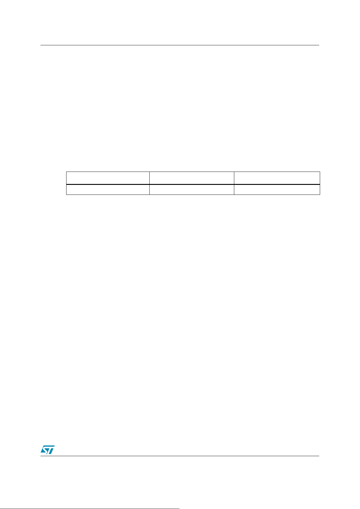
Figure 1. ST10F168 & ST10 F276 Flash Memories’ Mapping
Segment
number
14
13
12
11
10
9
8
7
6
5
4
3
2
1
0
STEAK TM Write/Erase Controller
ST10F168 mapping
03’8000 - 04’FFFF
02’0000 - 03’7FFF
01’8000 - 01’FFFF
01’4000 - 01’7FFF
01’0000 - 01’3FFF
00’0000 - 00’3FFF
Bank 3 : 96 Kbytes
Bank 2 : 96 Kbytes
Bank 1 H : 32 Kbytes
Alternate Flash Area
Alternate Flash Area
External memory+IRAM
Bank 1L : 16 Kbytes
Bank 0 : 16 Kbytes
0E’0000 - 0E’FFFF
0D’0000 - 0D’FFFF
0C’0000 - 0C’FFFF
0B’0000 - 0B’FFFF
0A’0000 - 0A’FFFF
09’0000 - 09’FFFF
08’0000 - 08’FFFF
07’0000 - 07’FFFF
06’0000 - 06’FFFF
05’0000 - 05’ FFFF
04’0000 - 04’FFFF
03’0000 - 03’FFFF
02’0000 - 02’FFFF
01’8000 - 01’FFFF
01’0000 - 01’7FFF
00’8000 -00’FFFF 00’8000 -00’FFFF
00’4000 - 00’7FFF00’4000 - 00’7FFF
00’2000 - 00’3FFF
00’0000 - 00’1FFF
ST10F276 Mapping
Reserved for Flash registers
B3F0 : 64KB
B2F1 : 64KB
B2F0 : 64KB
B1F1 : 64KB
B1F0 : 64KB
B0F9 : 64KB
B0F8: 64KB
B0F7: 64KB
B0F6: 64KB
B0F5: 64KB
B0F4: 32KB
Alternate Flash Area
External memory + IRAM
B0F2:8KB & B0F3: 8KB
B0F1:8KB
B0F0:8KB
B3F1: 64KB
B2F2: 64KB
Note: On the ST10F168, Bank 0 and Bank 1L may be remapped from segment 0 to segment 1 by
setting SYSCON.ROMS1.
On the ST10F276, sectors in segment 0 may be remapped to segment 1 by setting
SYSCON.ROMS1.
9/33
Page 10
Modified features AN2169
1.5 A/D converter
The Analog Digital converter has been re-designed between the ST10F168 and ST10F276.
The ST10F276 still provides an Analog / Digital Converter with 10-bit resolution and a sample &
hold circuit on-chip.
1.5.1 Hardware / Software impact: conversion timing control
The A/D converter is not fully compatible versus ST10F168 (timing and programming model).
As for the ST10F168, the sample time ( for loading the capacitors) and the conversion time are
programmable and can be adjusted to the external circuitry. The total conversion time is
compatible with the formula used for ST10F168, while the meaning of the bit fields ADCTC and
ADSTC is no longer compatible.
Table 3. ST10F276 Conversion timing table
ADCTC ADSTC Sample Comparison Extra Total Conversion
00 00 TCL * 120 TCL * 240 TCL * 28 TCL * 388
00 01 TCL * 140 TCL * 280 TCL * 16 TCL * 436
00 10 TCL * 200 TCL * 280 TCL * 52 TCL * 532
00 11 TCL * 400 TCL * 280 TCL * 44 TCL * 724
11 00 TCL * 240 TCL * 120 TCL * 52 TCL * 772
11 01 TCL * 280 TCL * 560 TCL * 28 TCL * 868
11 10 TCL * 400 TCL * 560 TCL * 100 TCL * 1060
11 11 TCL * 800 TCL * 560 TCL * 52 TCL * 1444
10 00 TCL * 480 TCL * 960 TCL * 100 TCL * 1540
10 01 TCL * 560 TCL * 1120 TCL * 52 TCL * 1732
10 10 TCL * 800 TCL * 1120 TCL * 196 TCL * 2116
10 11 TCL * 1600 TCL * 1120 TCL * 164 TCL * 2884
1.5.2 Hardware impact
Table 4. ADC differences
Parameter Symbol
Analog Reference
voltage
Reference supply
current
running mode
power-down mode
V
AREF
I
AREF
Limit values for
ST10F168
min. max. min. max.
+ 0.1
4.0
-
-
V
DD
Limit values for ST10F276
4.5
-
-
VDD + 0.1
5000
1
Unit
V
µA
10/33
Page 11

AN2169 Modified features
Parameter Symbol
ADC Input capacitance
Not sampling P5
Sampling P5
Not sampling P1
Sampling P1
Sample time
Total Unadjusted Error
Por t5
Port1 - No overload
Port1 - Overload
Differential Nonlinearity DNL -1 +1 LSB
Integral Nonlinearity INL -1.5 +1.5 LSB
Offset Error OFS -1.5 +1.5 LSB
1.5.3 Software impact
Self-calibration and ADC initialization routine
C
AIN
t
S
TUE
Limit values for
ST10F168
min. max. min. max.
-
-
-
-
48 TCL 1536 TCL 120 TCL 1600 TCL us
-2.0 +2.0
33
33
-
-
Limit values for ST10F276
+ CP2 +C
C
P1
-
-
-
-
-2.0
-5.0
+7.0
7
10.5
9
12.5
+2.0
+5.0
+7.0
Unit
S
pF
LSB
An automatic self-calibration adjusts the ADC module to process parameter variations at each
reset event. After reset, the busy flag (read-only) ADBSY is set because the self-calibration is
ongoing. The duration of self-calibration depends on the CPU clock: it takes up to 40.629 ± 1
clock pulses. The user shall poll this bit to know when the self-calibration is done and then
initialize the ADC module.
This self-calibration is seen by the ST10F276 as a conversion and thus bit ADCIR is set. The
software should perform a dummy read of the ADDAT register and clear the ADCIR and
ADCEIR flag before configuring the ADC module and starting the first conversion.
New bit ADOFF, bit 6 of ADCON register
ADCON (FFA0h / A0h)
SFR
Reset Value: 0000h
15 14 13 12 11 10 9 8 7 6 5 4 3 2 1 0
ADCTC ADSTC ADCTC ADCIN ADWR ADBSY ADST ADOFF ADM ADCH
RW RW RW RW RW RW RW R RW RW RW RW RW RW RW RW
Bit Function Comment
ADOFF: ADC Disable
6
0: Analog circuitry of A/D converter is on
1: Analog circuitry of A/D converter is turned off (no
consumption)
New bit only for the ST10F276.
Reserved for the ST10F168.
11/33
Page 12

Modified features AN2169
The bit 6 of ADCON register, reserved in the previous ST10 devices, has now the function of
enabling or disabling the ADC. By default this bit is cleared and the ST10F276 is compatible
with the ST10F168.
Additional analog channels on Port1
A new multiplexer selects between up to 16 or 8 analog input channels (alternate functions of
Port 5 and Port1). The selection of the Port1 or Port5 as input of the ADC is made via bit
ADCMUX, bit 0 of XMISC register.
XMISC (EB46h)
XREG
Reset Value: --00h
1514131211109876543210
VREG
------------
Bit Function
ADCMUX
0
0: default configuration, analog inputs on port P5.y can be converted
1: analog inputs on port P1.z can be converted, only 8 channel can be managed
CANCK2CANPARADCM
OFF
rw rw rw rw
UX
By default the multiplexer selects the Port5, so there is no impact on the software with regard to
a ST10F168 implementation.
1.6 PLL and on-chip main oscillator
In order to reach the new frequency range, the PLL multiplication factors have been changed.
Table 5. ST10F168 vs ST10F276 PLL ratio
ST10F168 ST10F276 ST10F276 ST10F276
P0.15-13
(P0H.7-5)
111
110
101
100
011
010
PLL factor
f
= f
CPU
F
XTAL
F
XTAL
F
XTAL
F
XTAL
F
XTAL
F
XTAL
* F
XTAL
f
CPU
* 4 F
* 3 F
* 2 F
* 5 F
* 1 F
* 1.5 F
PLL factor
= f
XTAL
* 4
XTAL
* 3
XTAL
* 8
XTAL
* 5
XTAL
* 1
XTAL
* 10
XTAL
* F
Input Frequency Range
(MHz)
Low Power
Oscillator
Wide Swing
Oscillator
Notes
4 to 8 4 to 8 Default configuration
5.3 to 8 5.3 to 10.6
4 to 8 4 to 8
6.4 to 8 6.4 to 12
1 to 64 1 to 64 Direct Drive
4 to 6.4 4 to 6.4
12/33
Page 13

AN2169 Modified features
ST10F168 ST10F276 ST10F276 ST10F276
P0.15-13
(P0H.7-5)
001
000
PLL factor
f
= f
CPU
F
XTAL
F
XTAL
* F
XTAL
f
CPU
/ 2 F
* 2.5 F
PLL factor
= f
XTAL
/ 2
XTAL
* 16
XTAL
Input Frequency Range
* F
Low Power
Oscillator
4 to 8 4 to 12
44
(MHz)
Wide Swing
Oscillator
Notes
CPU clock via prescaler
13/33
Page 14

New functionalities AN2169
2 New functionalities
2.1 CAN module
The ST10F168 has only one CAN module of the B-CAN type.
The ST10F276 has two CAN modules of the C-CAN type.
The C-CAN cells provide additional Message Objects and new functionalities like Time
Triggered Protocol capability. The main difference is that the Message Objects are no longer
directly accessed as memory but are available through a Message Interface. This changes the
programming model of the modules.
2.1.1 Hardware impact
None.
2.1.2 Software impact
Re-write the CAN Drivers
2.2 Real time clock
This is a new functionality of the ST10F276.
The Real Time Clock is an independent timer. Its clock is directly derived from the clock
oscillator so that it can keep on running even in idle or power down mode (if enabled).
2.2.1 Hardware impact
None
2.2.2 Software impact
None. By default, this peripheral is disabled.
2.3 MAC unit
This Multiply and Accumulate Unit is a feature added on the ST10F276.
2.3.1 Hardware impact
None
2.3.2 Software impact
None
14/33
Page 15

AN2169 New functionalities
2.4 Additional X-peripherals
Some peripherals have been added on the ST10F271-B. They are mapped on the X-Bus and
are linked to additional alternate functions of some ports of the ST10F271-B.
The additional X-Peripherals are the following:
● An additional SSC called XSSC.
● An additional ASC called XASC.
● An additional 4-channel PWM called XPWM .
● An I2C interface
● An additional C-CAN Interface
Note: Some restrictions and functional differences between the original peripherals and XASC, XSSC
and XPWM exist. Those differences impact interrupts management, related IO configuration
and peripherals activation.
2.4.1 Hardware impact
None if the additional peripherals are not used.
2.4.2 Software impact
None if the additional peripherals are not used. As they are X-peripherals, they can be enabled
/ disabled via the XPERCON and the SYSCON registers.
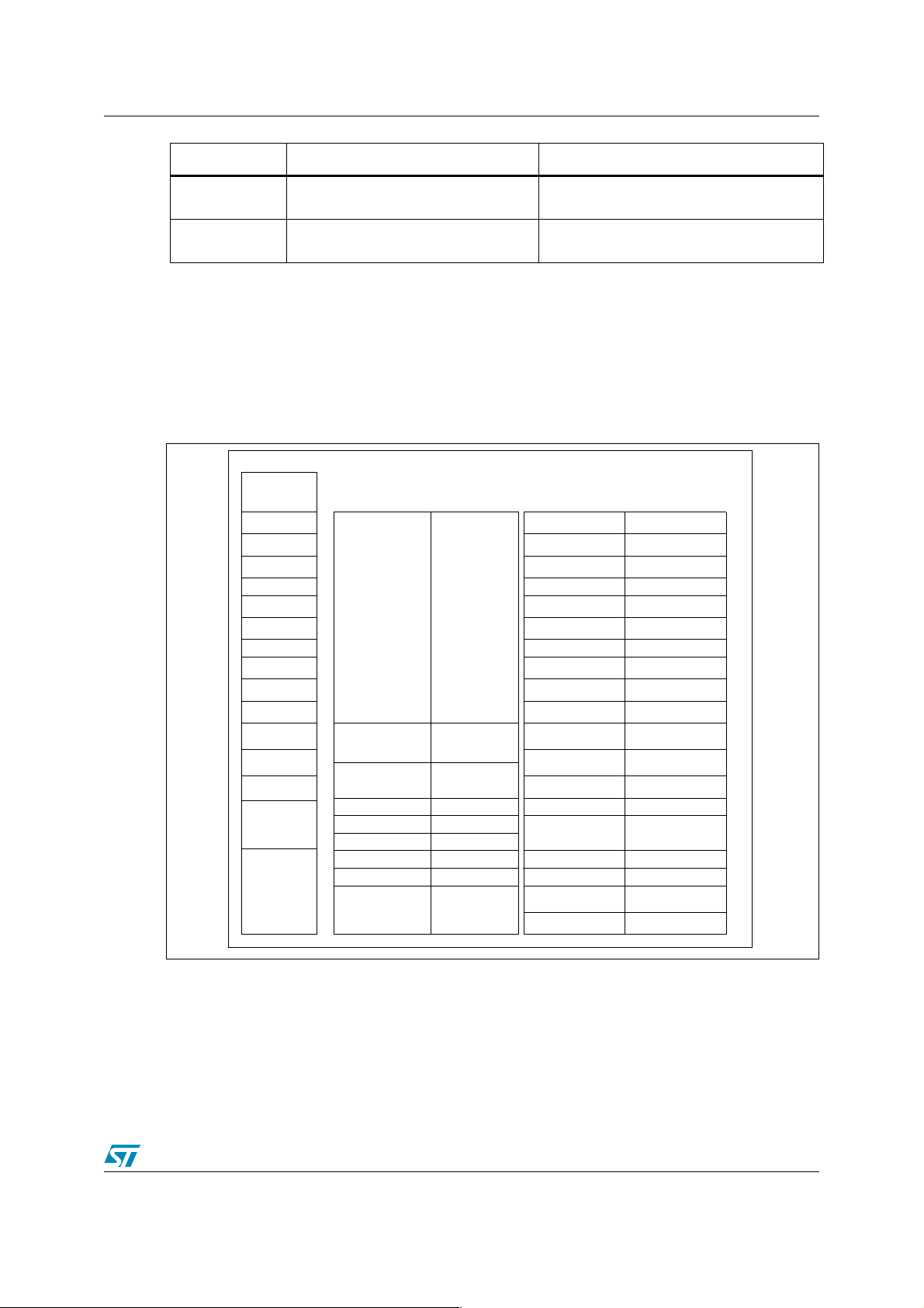
2.5 New multiplexer for X-interrupts
The limited number of X-Bus interrupt lines of the present ST10 architecture, imposes some
constraints on the implementation of the new functionalities. In particular, the additional XPeripherals XSSC, XASC, XI2C and XPWM need some resources to implement interrupt and
PEC transfer. For this reason, a complex but very flexible multiplexed structure for the interrupt
is proposed. In next figure, the principle is represented through a simple diagram, which shows
the basic structure replicated for each of the four X-interrupt vectors (XP0INT, XP1INT, XP2INT
and XP3INT).
It is based on a new 16-bit register XIRxSEL (x=0,1,2,3), divided in two portions:
● Byte High (XIRxSEL[15:8]) Interrupt Enable bits
● Byte Low (XIRxSEL[7:0]) Interrupt Flag bits
When different sources submit an interrupt request, the enable bits (Byte High of XIRxSEL
register) define a mask which controls which sources will be associated with the unique
available vector. If more than one source is enabled to issue the request, the service routine will
have to take care to identify the real event to be serviced. This can easily be done by checking
the flag bits (Byte Low of XIRxSEL register). Note that the flag bit can provide information about
events which are not currently serviced by the interrupt controller (when masked through the
enable bits), allowing an effective software management also in absence of the possibility to
serve the related interrupt request: a period polling of the flag bits may be implemented inside
the user application.
15/33
Page 16

New functionalities AN2169
Figure 2. X-Interrupt basic structure
70
Flag[7:0]
IT Source 7
IT Source 6
IT Source 5
IT Source 4
IT Source 3
IT Source 2
IT Source 1
IT Source 0
XIRxSEL[7:0] (x = 0, 1, 2, 3)
XPxIC.IR (x = 0, 1, 2, 3)
Enable[7:0]
15 8
XIRxSEL[15:8] (x = 0, 1, 2, 3)
Table 6. X-Interrupt detailed mapping
XP0INT XP1INT XP2INT XP3INT
CAN1 Interrupt X X
CAN2 Interrupt X X
I2C Receive X X X
I2C Transmit X X X
I2C Error X
SSC1 Receive X X X
SSC1 Transmit X X X
SSC1 Error X
ASC1 Receive X X X
ASC1 Transmit X X X
ASC1 Transmit Buffer X X X
ASC1 Error X
PLL Unlock / OWD X
PWM1 Channel 3...0 X X
2.5.1 Hardware impact
None.
2.5.2 Software impact
The XIRxSEL registers must be configured.
If none of the new X-Peripherals are used, i.e. only the X-Peripherals that were already present
on the ST10F168 are used, the following configuration can be used:
16/33
Page 17

AN2169 New functionalities
● XIR0SEL = 0x0100, only CAN1 interrupt is enabled and will generate an interrupt to the
ST10 through XP0IC
● XIR2SEL = 0x0, not used
● XIR3SEL = 0x2000, only PLL unlock interrupt is enabled and will generate an interrupt to
the ST10 through XP3IC.
Then, in the interrupt routines associated to the XPxIC, the respective flag in XIRxSEL register
must be cleared. Since the XIRxSEL registers are not bit addressable, a pair of registers (a pair
for each XIRxSEL) is provided to allow setting and clearing the bits of XIRxSEL without risking
to overwrite requests coming after reading the register and before writing it. Therefore the
following registers must be written to clear the flags:
● in the CAN1 interrupt routine, XIR0CLR (@ EB14h) = 0x0001
● in the PLL unlock interrupt routine, XIR3CLR (@ EB44h) = 0x0020
Additional information on the X-Interrupt multiplexer structure
Figure 2 shows that the X-Interrupt sources are connected to the interrupt request flag of the
XIRxSEL registers and to the XPxIR request flag via an AND gate with the enable bit. This AND
gate is activated by a transition on the Interrupt source line and not by the latched value in the
XIRxSEL register meaning:
● A transition on the IT source line will generate an interrupt to the ST10 core if the source is
enabled.
● Writing to an interrupt request flag in a XIRxSEL register will not generate an interrupt to
the ST10 core.
Example: If XIR0SEL = 0x0100: CAN1 interrupt enabled on XP0IC interrupt
To trigger by software the CAN1 interrupt routine with XP0IC register, the following code must
be used:
XIR0SET = 0x0001;/* Set CAN1 interrupt request Flag in XIR0SEL
register */
XP0IC = XP0IC | 0x0080;/* Set XP0IR flag and generate an interrupt
routine to the ST10 */
Executing only the first line will only set the flag in the XIR0SEL register but will not be seen by
the AND gate and can not set the XP0IR flag.
2.6 Programmable divider on CLKOUT
A specific register mapped on the XBUS allows to choose the division factor on the CLKOUT
signal (P3.15).
XCLKOUTDIV (E902h)
XBUS
Reset Value: --00h
1514131211109876543210
-------- DIV
rw rw rw rw rw rw rw rw
17/33
Page 18

New functionalities AN2169
Bit Function
7:0
DIV
Fclkout = Fcpu / (DIV + 1)
2.6.1 Hardware impact
None.
2.6.2 Software impact
None if only CLOCKOUT is needed.
When CLKOUT function is enabled by setting the bit CLKEN of register SYSCON, by default
the CPU clock is output on P3.15. To have access to XCLKOUTDIV register, and thus program
the clock pre-scaling factor, the bit XMISCEN of XPERCON and XPEN of SYSCON registers
must be set.
18/33
Page 19

AN2169 Modified registers
3 Modified registers
3.1 WDTCON register
Some bits have been added for the ST10F276. Each of the different reset sources is indicated
in the WDTCON register of the ST10F276. The indicated bits are cleared with the EINIT
instruction. It is thus possible to identify the reset during the initialization phase.
ST10F168: WDTCON (FFAEh / D7h)
SFR
Reset Value: --05h
15 14 13 12 11 10 9 8 7 6 5 4 3 2 1 0
WDTREL
-
RW RW RW RW RW RW RW RW --- RRW
ST10F276: WDTCON (FFAEh / D7h)
SFR
- - - WDTR WDTIN
Reset Value: -005h
15 14 13 12 11 10 9 8 7 6 5 4 3 2 1 0
WDTREL PONR LHWR SHWR SWR WDTR WDTIN
RW RW RW RW RW RW RW RW RW RW HR HR HR HR HR RW
Bit Function
15:8 WDTREL: Watchdog Timer Reload Value (for the high byte)
5
(ST10F276)
4
(ST10F276)
3
(ST10F276)
2
(ST10F276)
PONR: Power-on (Asynchronous) Reset Indication Flag
Set by the Input RSTIN if a power-On condition has been detected.
Cleared by the EINIT instruction
LHWR: Long Hardware Reset indication Flag
Set by the input RSTIN
Cleared by the EINIT instruction
SHWR: Short Hardware Reset indication Flag
Set by the input RSTIN
Cleared by EINIT instruction
SWR: Software Reset Indication Flag
Set by the SRST execution
Cleared by the EINIT instruction
19/33
Page 20

Modified registers AN2169
Bit Function
WDTR: Watchdog Timer Reset Indication Flag
1
0
Set by the watchdog timer on an overflow.
Cleared by a hardware reset or by the SRVWDT instruction.
WDTIN: Watchdog Timer Input Frequency Selection
0:Input frequency is Fcpu /2
1:Input frequency is Fcpu /128
Note: 1 More than one RESET indication flag may be set. After EINIT, all flags are cleared.
2 Power-on is detected when a rising edge from VDD=0 V to VDD<2.0 V is recognized.
3.1.1 Hardware impact
None.
3.1.2 Software impact
None if the ST10F168 software was masking the non-implemented bits.
3.2 PICON register
Some bits have been added, and some suppressed in this register for the ST10F276.
The port Input Control register PICON is used to select between TTL and CMOS-like input
thresholds.
The CMOS-like input thresholds are defined above the TTL levels and feature a defined
hysteresis to prevent the inputs from toggling while the respective input signal level is near the
thresholds.
On the ST10F168, this functionality is available for pins of port 2, port3, port7 and port8 and the
hysteresis level is 300 mV for CMOS levels.
In the ST10F276, this functionality has been added for the pins of port 4 and port 6.
Moreover the default hysteresis is now 500 mV for TTL levels and is 800 mV for CMOS levels.
ST10F168: PICON (F1C4h /E2h)
ESFR
Reset Value: 0000h
15 14 13 12 11 10 9 8 7 6 5 4 3 2 1 0
P8LOUT P7LOUT - P3HOUT P3LOUT P2HOUT P2LOUT P8LIN P7LIN P3HIN P3LIN P2HIN P2LIN
RW RW RW RW RW RW RW RW RW RW RW RW
ST10F276: PICON (F1C4h / E2h)
ESFR
20/33
Page 21

AN2169 Modified registers
Reset Value: 0000h
15 14 13 12 11 10 9 8 7 6 5 4 3 2 1 0
- - - - - - - - P8LIN P7LIN P6LIN P4LIN P3HIN P3LIN P2HIN P2LIN
RW RW RW RW RW RW RW RW
Bit Name Function
Port x Low Byte Input Level Selection
PxLIN
PxHIN
PxLOUT
PxHOUT
0: Pins Px.7..0 switch on standard TTL input levels
1: Pins Px.7..0 switch on CMOS input levels
Port x High Byte Input Level Selection
0: Pins Px.15..8 switch on standard TTL input levels
1: Pins Px.15..8 switch on CMOS input levels
Port x Low Byte Output Driver Characteristic selection
0: Pins Px.7...0 output driver strength is reduced after reaching VOL or
VOH
1: Pins Px.7...0 output drive is not reduced after reaching VOL or VOH
Port x High Byte Output Driver Characteristic selection
0: Pins Px.15...8 output driver strength is reduced after reaching VOL or
VOH
1: Pins Px.15...8 output drive is not reduced after reaching VOL or VOH
Only for
ST10F168
Only for
ST10F168
3.2.1 Hardware impact
The CMOS levels of the 2 devices are slightly different, therefore the circuitry must be checked
to verify that the new levels can still match the requirements.
3.2.2 Software impact
The high byte of the PICON register is reserved on the ST10F276. Check that the ST10F168
was not writing in bits P4LIN and P6LIN of PICON which are no longer reserved on the
ST10F276.
3.3 IDCHIP register
A new field has been added inside the IDCHIP register to distinguish the different peripheral
options.
ST10F168: IDCHIP (F07Ch)
ESFR
Reset Value: 10DXh
15 14 13 12 11 10 9 8 7 6 5 4 3 2 1 0
CHIPID REVID
RRRR R R R R R R RRRRRR
21/33
Page 22

Modified registers AN2169
ST10F276: IDCHIP (F07Ch)
ESFR
Reset Value: 114Xh
15 14 13 12 11 10 9 8 7 6 5 4 3 2 1 0
PCONF CHIPID REVID
RRRR R R R R R R RRRRRR
Bit Name Function
ST10 Module Revision Identifier (Full Mask Set revision)
01h: Rev. A (First main revision)
REVID
CHIPID
PCONF
02h: Rev. B (Second main revision)
:
0Fh: Rev. P
ST10 Module Identifier
0A8: ST10F168 identifier (168d = 0A8h)
114h: ST10F276 identifier (276d = 114h)
Peripheral Configuration
00: (E) Enhanced (ST10F276)
01: (B) Basic
10: (D) Dedicated
11: reserved
3.3.1 Hardware Impact
None.
3.3.2 Software Impact
None.
22/33
Page 23

AN2169 New registers
4 New registers
This section presents new registers that have to be considered when porting an application
running on the ST10F168 onto the ST10F276.
4.1 XPERCON register
The ST10F276 has a new register named XPERCON that allows the XBUS peripherals to be
separately selected for being visible to the user by means of corresponding bits. If not selected
(not activated with a bit of XPERCON) before the XPEN bit in SYSCON is set, the
corresponding address space, port pins and interrupts are not occupied by the peripheral, and
thus this peripheral is not visible and not available.
ST10F276: XPERCON (F024h / 12h)
SFR
Reset Value: -005h
15 14 13 12 11 10 9 8 7 6 5 4 3 2 1 0
---- -XMISCENXI2CENXSSCENXASCENXPWMENXFLASHENRTCENXRAM2ENXRAM1ENCAN2ENCAN1
RW RW RW RW RW RW RW RW RW RW RW
EN
Bit Function
15:11 Reserved
XMISCEN: XBUS Additional Features Enable Bit
10
9
8
7
6
5
0: Accesses to the Additional Miscellaneous Features is disabled.
1: The Additional Features are enabled and can be accessed.
XI2CEN: XI 2 C Enable Bit
0: Accesses to the on-chip XI 2 C are disabled, external access performed.
1: The on-chip XI 2 C is enabled and can be accessed.
XSSCEN: XSSC Enable Bit
0: Accesses to the on-chip XSSC are disabled, external access performed.
1: The on-chip XSSC is enabled and can be accessed.
XASCEN: XASC Enable Bit
0: Accesses to the on-chip XASC are disabled, external access performed.
1: The on-chip XASC is enabled and can be accessed.
XPWMEN: XPWM Enable
0: Accesses to the on-chip XPWM module are disabled, external access performed.
1: The on-chip XPWM module is enabled and can be accessed.
XXFLASHEN: FLASH Enable Bit
0: Accesses to the on-chip XFLASH are disabled, external access performed.
1: The on-chip XFLASH is enabled and can be accessed.
23/33
Page 24

New registers AN2169
Bit Function
RTCEN: RTC Enable Bit
4
3
2
1
0
0: Accesses to the on-chip Real Time Clock are disabled, external access performed.
1: The on-chip Real Time Clock is enabled and can be accessed.
XRAM2EN: XRAM2 Enable Bit
0: Accesses to the on-chip XRAM2 block are disabled, external access performed.
1: The on-chip XRAM2 is enabled and can be accessed.
XRAM1EN: XRAM1 Enable Bit
0: Accesses to the on-chip XRAM1 block are disabled, external access performed.
1: The on-chip XRAM1 is enabled and can be accessed.
CAN2EN: CAN2 Enable Bit
0: Accesses to the CAN2 XPeripheral and its functions are disabled (P4.4 and P4.7 pins
can be used as general purpose IOs)
1: The CAN2 X-Peripheral is enabled and can be accessed.
CAN1EN: CAN1 Enable Bit
0: Accesses to the CAN1 XPeripheral and its functions are disabled (P4.5 and P4.6 pins
can be used as general purpose IOs)
1: The CAN1 X-Peripheral is enabled and can be accessed.
4.1.1 Hardware impact
None.
4.1.2 Software impact
The value has to be changed from its default reset one to match XRAM size compatibility. Refer
to XRAM section for more details.
4.2 XPEREMU register
This register has been added as a write-only register.
ST10F276: XPEREMU (EB7Eh)
XREG
Reset Value: XXXXh
15 14 13 12 11 10 9 8 7 6 5 4 3 2 1 0
---- -XMISCENXI2CENXSSCENXASCENXPWMENXFLASHENXRTCENXRAM2ENXRAM1ENCAN2ENCAN1
---- - W W W W W W W W W WW
The bit description is exactly the same as XPERCON.
EN
4.2.1 Hardware Impact
None.
24/33
Page 25

AN2169 New registers
4.2.2 Software Impact
Once the XPEN bit of SYSCON register is set and at least one of the X-peripherals (except
memories) is activated, the register XPEREMU must be written with the same content of
XPERCON: this is mandatory in order to allow a correct emulation of the new set of features
introduced on X-BUS for the new ST10 generation. The following instructions must be added
inside the initialization routine:
if (SYSCON.XPEN && (XPERCON & 0x07D3))
then { XPEREMU = XPERCON }
Of course, XPEREMU must be programmed after XPERCON and after SYSCON, in such a
way the final configuration for X-Peripherals is stored in XPEREMU and used for the emulation
hardware setup.
4.3 EXISEL register
This register, standing for External Interrupt source selection, has been added in the
ST10F276.
The purpose of this new register is to select the interrupt sources of the fast external interrupts
among the other peripherals. For example, the CANy controller receive signal (CANy_RxD) can
be used to interrupt the system(y=1,2).
ST10F276: EXISEL (F1DAh / EDh)
SFR
Reset Value: -005h
15 14 13 12 11 10 9 8 7 6 5 4 3 2 1 0
EXI7SS EXI6SS EXI5SS EXI4SS EXI3SS EXI2SS EXI1SS EXI0SS
RW RW RW RW RW RW RW RW RW RW RW RW RW RW RW RW
Bit name Function
External Interrupt x source Selection (x=7..0)
00: Input from associated Port 2 pin.
EXIxSS
EXIxSS Port 2 pin Alternate source
01: Input from "alternate source".
10:Input from associated Port 2 pin logically ORed with "alternate source".
11:Input from associated Port 2 pin logically ANDed with "alternate source".
0 P2.8 CAN1_RxD P4.5
1 P2.9 CAN2_RxD / SCL P4.4
2 P2.10 RTC_secIT Internal MUX
3 P2.11 RTC_alarmIT Internal MUX
4..7 P2.12..P2.15 Not used (zero) -
25/33
Page 26

New registers AN2169
4.4 Additional Ports Input Control: XPICON register
The possibility to select between TTL and CMOS-like input thresholds has been extended to
the Ports 0, 1 and 5.
ST10F276: XPICON (EB26h)
XREG
Reset Value: --00h
15 14 13 12 11 10 9 8 7 6 5 4 3 2 1 0
- - - - - - - - - - P5HIN P5LIN P1HIN P1LIN P0HIN P0LIN
RW RW RW RW RW RW
Bit Function
P5HIN: Port 5 High Byte Input Level Selection
5
4
3
2
1
0
0: Pins P5.15..8 switch on standard TTL input levels
1: Pins P5.15..8 switch on CMOS input levels
P5LIN: Port 5 Low Byte Input Level Selection
0: Pins P5.7..0 switch on standard TTL input levels
1: Pins P5.7..0 switch on CMOS input levels
P1HIN: Port 1 High Byte Input Level Selection
0: Pins P1.15..8 switch on standard TTL input levels
1: Pins P1.15..8 switch on CMOS input levels
P1LIN: Port 1 Low Byte Input Level Selection
0: Pins P1.7..0 switch on standard TTL input levels
1: Pins P1.7..0 switch on CMOS input levels
P0HIN: Port 0 High Byte Input Level Selection
0: Pins P0.15..8 switch on standard TTL input levels
1: Pins P0.15..8 switch on CMOS input levels
P0LIN: Port 0 Low Byte Input Level Selection
0: Pins P0.7..0 switch on standard TTL input levels
1: Pins P0.7..0 switch on CMOS input levels
Reset
Val ue
0
0
0
0
0
0
4.4.1 Hardware impact
None.
4.4.2 Software impact
None.
26/33
Page 27

AN2169 New registers
4.5 XMISC register
ST10F276: XMISC (EB46h)
XREG
Reset Value: 0000h
151413121110987654 3 2 1 0
------------VREG
------------RWRWRWRW
Bit Function
15:4 Reserved
VREGOFF: Main Voltage Regulator disable in Power-Down mode
3
2
1
0
0: On-chip Main Regulator is held active when Power-Down mode is entered
1: On-chip Main Regulator is turned off when Power-Down mode is entered
CANCK2: CAN Clock divider by 2 disable
0: Clock provided to CAN modules is CPU clock divided by 2 (mandatory when F
higher than 40MHz)
1: Clock provided to CAN modules is directly CPU clock
CANPAR: CAN Parallel Mode Selection
0: CAN2 is mapped on P4.4/P4.7, while CAN1 is mapped on P4.5/P4.6
1: CAN1 and CAN2 are mapped in parallel on P4.5/P4.6. This is effective only if both
CAN1 and CAN2 are enabled through setting of bits CAN1EN and CAN2EN in
XPERCON register. If CAN1 is disabled, CAN2 remains on P4.4/P4.7 even if bit CANPAR
is set.
ADCMUX: Port1L ADC Channels Enable
0: Analog inputs on port P5.y can be converted (default configuration)
1: Analog inputs on port P1.z can be converted. Only 8 channels can be managed
OFF
CAN
CK2
CAN
PAR
CPU
ADC
MUX
is
4.5.1 Hardware impact
None.
4.5.2 Software impact
None.
4.6 Emulation dedicated registers
A set of additional four registers are implemented for emulation purpose only. Similarly to
XPEREMU, they are write only registers.
XEMU0 (00’EB76h)
XEMU1 (00’EB78h)
XEMU2 (00’EB7Ah)
XEMU3 (00’EB7Ch)
27/33
Page 28

New registers AN2169
These registers are used by emulators. They have no user action on the ST10F276.
4.6.1 Hardware impact
None.
4.6.2 Software impact
None.
28/33
Page 29

AN2169 Electrical characteristics
5 Electrical characteristics
5.1 DC characteristics
5.1.1 Absolute maximum ratings
They are the same.
5.1.2 DC characteristics
Overview of the DC characteristics
The pads of the ST10F276 have been redesigned according to the new technology and
therefore the characteristics are different. Users should verify the DC characteristics.
The table below lists the parameters that might have the biggest impact.
ST10F168 Limit Values ST10F276 Limit Values
Parameter Symbol
min. max. min. max.
Unit
Input low voltage
Input low voltage
(RSTIN, EA,
NMI, and RPD)
Input low voltage
(XTAL1 and
XTAL3)
Input high
voltage
Input high
voltage (RSTIN,
EA, NMI, and
RPD)
Input high
voltage XTAL1
Input Hysteresis HYS
Input Hysteresis
RSTIN, EA, NMI
Output low
voltage
Output low
voltage (all other
outputs)
Output high
voltage
Output high
voltage (all other
outputs)
VIL SR
VILS SR
VIL1 SR N.A. N.A. -0.3 0.3 VDD V
VIL2 SR -0.3 0.3 VDD V
VIH SR
VIHSSR
VIH1SR 0.6 VDD
VIH2SR 0.7 VDD VDD + 0.5 0.7 VDD VDD + 0.3 V
VHYS1CC 800 mV
VOL C C
VOL1CC – 0.45 / Iol = 1.6mA –
VOH CC
VOH1CC
-0.5
-0.5
0.2 VDD + 0.9
0.8 VDD - 0.2
N.A.
300, special threshold
PORT0, PORT1, Port
4, ALE, RD, WR,
BHE, CLKOUT,
RSTOUT
0.9VDD / Ioh = -0.5
mA
2.4 / Ioh = -2.4 mA
0.9VDD / Ioh = -0.25
mA
2.4 / Ioh = -1.6 mA
0.2 VDD - 0.1
2.0, (special
threshold)
VDD + 0.5
VDD + 0.5,( special
threshold )
VDD + 0.5, (special
threshold)
-
0.45 / Iol = 2.4mA
PORT0, PORT1,
Port 4, ALE, RD,
WR, BHE, CLKOUT,
RSTOUT
–
-0.3
-0.3
2.0
0.7 VDD
0.7 VDD VDD + 0.3 V
400
750
PORT6, ALE,
CLKOUT, WR, READY,
BHE, RD, RSTOUT,
RSTIN
VDD - 0.8 / Ioh = -8
mA
VDD -0.08 / Ioh = -1
mA
VDD - 0.8 / Ioh = -4 mA
VDD -0.08 / Ioh = -0.5
mA
0.8
0.3 VDD
VDD + 0.3
VDD + 0.3
-mV
0.4 / Iol = 8mA
0.05 / Iol = 1mA
0.4 / Iol = 4 mA
0.05 / Iol = 0,5 mA
PORT6, ALE,
CLKOUT, WR,
READY, BHE, RD,
RSTOUT, RSTIN
–V
V
V
V
V
V
29/33
Page 30

Electrical characteristics AN2169
ST10F168 Limit Values ST10F276 Limit Values
Parameter Symbol
Unit
min. max. min. max.
Input leakage
current (Port 5)
Input leakage
current (all
other)
Input leakage
current (P2.0)
Input leakage
current (RPD)
Overload current
(P2.0)
IOZ1CC –
IOZ2CC – ±1 / 0 V <VIN< VDD – ±0.5 uA
IOZ3CC – - –
IOZ4CC – - – ±3 uA
IOV2CC – - –
± 500 / 0 V <VIN<
VDD
–± 200nA
-0.5
+1
-1
+5
uA
mA
30/33
Page 31

AN2169 References
6 References
The following documents were used to write this application note:
● ST10F168 Datasheet
● ST10F276 Datasheet
● AN1313 Application Note "Porting an application from the ST10F168 to the ST10F269"
31/33
Page 32

Revision history AN2169
7 Revision history
Table 7. Document revision history
Date Revision Changes
3-Jul-2006 1 Initial release.
32/33
Page 33

AN2169 Revision history
r
Please Read Carefully:
Information in this document is provided solely in connection with ST products. STMicroelectronics NV and its subsidiaries (“ST”) reserve the right to make changes, corrections,
modifications or improvements, to this document, and the products and services described herein at any time, without notice.
All ST products are sold pursuant to ST’s terms and conditions of sale.
Purchasers are solely responsible for the choice, selection and use of the ST products and services described herein, and ST assumes no liability whatsoever relating to the
choice, selection or use of the ST products and services described herein.
No license, express or implied, by estoppel or otherwise, to any intellectual property rights is granted under this document. If any part of this document refers to any third party
products or services it shall not be deemed a license grant by ST for the use of such third party products or services, or any intellectual property contained therein or considered
as a warranty covering the use in any manner whatsoever of such third party products or services or any intellectual property contained therein.
UNLESS OTHERWISE SET FORTH IN ST’S TERMS AND CONDITIONS OF SALE ST DISCLAIMS ANY EXPRESS OR IMPLIED WARRANTY WITH RESPECT TO THE
USE AND/OR SALE OF ST PRODUCTS INCLUDING WITHOUT LIMITATION IMPLIED WARRANTIES OF MERCHANTABILITY, FITNESS FOR A PARTICULAR
PURPOSE (AND THEIR EQUIVALENTS UNDER THE LAWS OF ANY JURISDICTION), OR INFRINGEMENT OF ANY PATENT, COPYRIGHT OR OTHER INTELLECTUAL
PROPERTY RIGHT.
UNLESS EXPRESSLY APPROVED IN WRITING BY AN AUTHORIZE REPRESENTATIVE OF ST, ST PRODUCTS ARE NOT DESIGNED, AUTHORIZED OR WARRANTED
FOR USE IN MILITARY, AIR CRAFT, SPACE, LIFE SAVING, OR LIFE SUSTAINING APPLICATIONS, NOR IN PRODUCTS OR SYSTEMS, WHERE FAILURE OR
MALFUNCTION MAY RESULT IN PERSONAL INJURY, DEATH, OR SEVERE PROPERTY OR ENVIRONMENTAL DAMAGE.
Resale of ST products with provisions different from the statements and/or technical features set forth in this document shall immediately void any warranty granted by ST fo
the ST product or service described herein and shall not create or extend in any manner whatsoever, any liability of ST.
ST and the ST logo are trademarks or registered trademarks of ST in various countries.
Information in this document supersedes and replaces all information previously supplied.
The ST logo is a registered trademark of STMicroelectronics. All other names are the property of their respective owners.
© 2006 STMicroelectronics - All rights reserved
STMicroelectronics group of companies
Australia - Belgium - Brazil - Canada - China - Czech Republic - Finland - France - Germany - Hong Kong - India - Israel - Italy - Japan - Malaysia - Malta - Morocco - Singapore
- Spain - Sweden - Switzerland - United Kingdom - United States of America
www.st.com
33/33
 Loading...