

Page 1

AN2164
Application note
Interfacing the ST10 with external memory
Introduction
The ST10 microcontrollers offer an addressable space of 16 Mbytes. The on-chip
peripherals, the on-chip RAM and Flash memory cover only a small fraction of this
addressable space leaving the remaining space to be used to interface external peripherals
and memories with the ST10.
This application note is divided into two parts. The first acts as a brief overview of features of
the ST10 external bus such as the EBC operating modes, port pins timing and maximum
addressable space.
The second part of the document describes how to connect external memory to the ST10.
In the sections contained in this part, the use of both demultiplexed and multiplexed buses is
considered, giving examples of word-wide and byte-wide memory.
This application note does not replace the ST10 user manuals or data sheets.
May 2007 Rev 1 1/14
www.st.com
Page 2

Contents AN2164
Contents
1 EBC overview . . . . . . . . . . . . . . . . . . . . . . . . . . . . . . . . . . . . . . . . . . . . . . 3
1.1 EBC operating modes . . . . . . . . . . . . . . . . . . . . . . . . . . . . . . . . . . . . . . . . 3
1.2 EBC Port pins control . . . . . . . . . . . . . . . . . . . . . . . . . . . . . . . . . . . . . . . . . 3
1.3 EA pin . . . . . . . . . . . . . . . . . . . . . . . . . . . . . . . . . . . . . . . . . . . . . . . . . . . . . 4
1.4 EBC timing . . . . . . . . . . . . . . . . . . . . . . . . . . . . . . . . . . . . . . . . . . . . . . . . . 4
1.5 EBC maximum addressable space . . . . . . . . . . . . . . . . . . . . . . . . . . . . . . 5
2 How to connect an external memory to the ST10 with a demultiplexed
bus 7
2.1 16-bit demultiplexed bus and word-wide memory example . . . . . . . . . . . . 7
2.2 16-bit demultiplexed bus and byte-wide memories example . . . . . . . . . . . 8
3 How to connect an external memory to the ST10 with a multiplexed bus
11
3.1 16-bit multiplexed bus and word-wide memory example . . . . . . . . . . . . . 11
3.2 16-bit multiplexed and byte-wide memories example . . . . . . . . . . . . . . . . 12
4 Revision history . . . . . . . . . . . . . . . . . . . . . . . . . . . . . . . . . . . . . . . . . . . 13
2/14
Page 3
AN2164 EBC overview
1 EBC overview
The ST10 External Bus Controller provides the user with a number of options:
● to enable the ST10 to be run entirely from external memory (code and/or data storage)
● to use combinations of on chip and external memories up to the 16 MBytes limit
● to access some internal resources (X-peripherals, XFlash, XRAM)
1.1 EBC operating modes
The ST10F27x offers the following operational modes:
● 16-/18-/20-/24- bit addresses and 16-bit data demultiplexed
● 16-/18-/20-/24- bit addresses and 16-bit data multiplexed
● 16-/18-/20-/24- bit addresses and 8-bit data demultiplexed
● 16-/18-/20-/24- bit addresses and 8-bit data multiplexed
The ST10 provides up to 5 CSx signals which can be programmed to operate in different
modes. Each CSx mode and characteristics are selected independently allowing the
possibility to interface the ST10 with different external resources.
CS0 operating mode is selected by hardware according to the fields BYTP0 and BYTP1
(P0L.6 and P0L.7).
CS1...CS4 operating modes are selected by software via the field BYTP in the
corresponding BUSCONx register.
For a detailed description of these modes, the ST10 EBC-related registers and their
configurations, refer to the ST10 user manuals.
1.2 EBC Port pins control
The ST10 external memory interface is implemented through 4 ports: P0, P1,P4 and P6 in
addition to some dedicated pins.
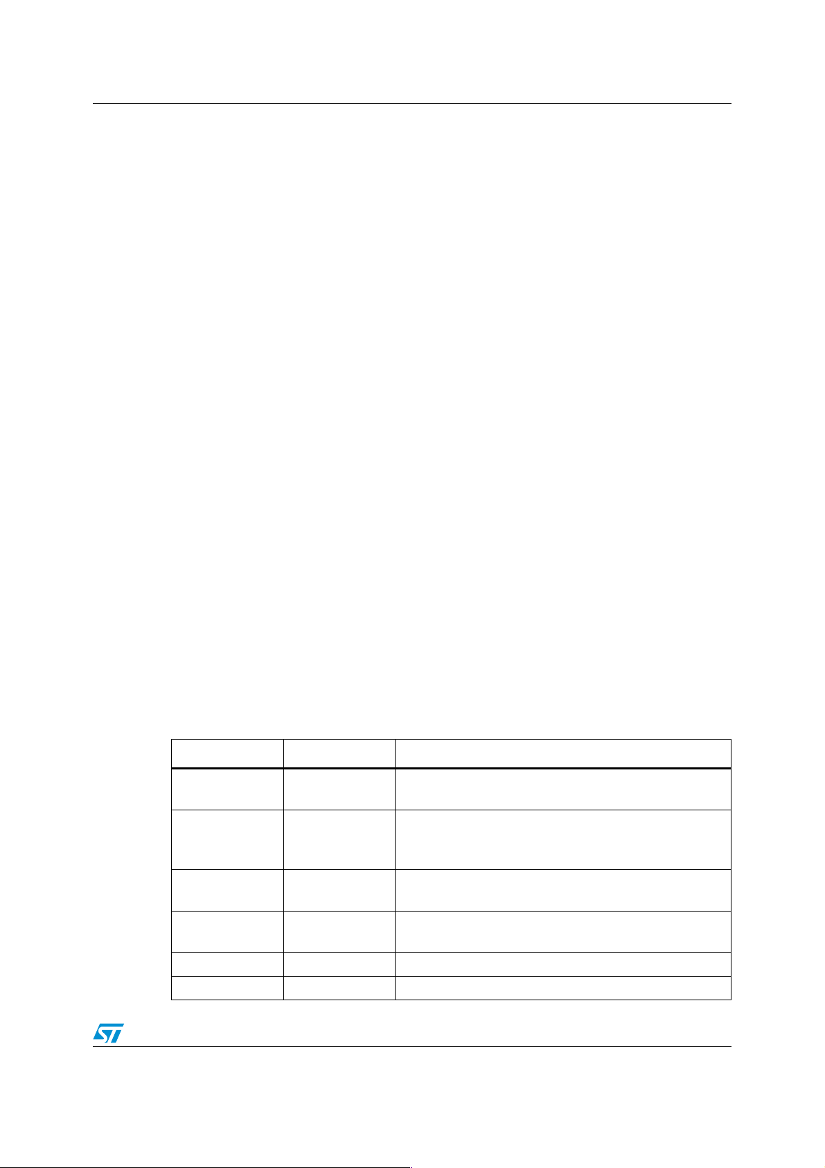
Table 1.
I/O Name Pin Number Function
P0L
AD0 .. AD7
P0H
AD8.. AD15
P1L
A0 .. A7
P1H
A8 .. A15
P4 85.. 92 O Address A16 .. A23 if needed
P6.0 .. P6.4 1 .. 5 Output Chip Select Enable CS0 .. CS4
ST10F27x EBC I/O port lines.
100 .. 107
108, 111.. 117
118 ..125 O address in 8-/16- bit demultiplexed bus
128 .. 135 O address in 8-/16- bit demultiplexed bus
I/O Data in 8-/16- bit demultiplexed bus
O address & I/O Data 8-/16- bit in multiplexed bus
I/O Data in 16-bit demultiplexed bus
O address in 8-bit multiplexed bus
O address and I/O data in 16-bit demultiplexed bus
3/14
Page 4

EBC overview AN2164
I/O Name Pin Number Function
EA 99 External Memory Access Enable pin
ALE 98 Address Latch Enable Output
READY 97 Ready input level
WR/WRL 96 External Write Enable/ External Write low byte Enable
RD 95 External Read Enable
HOLD 6 External Master Hold Request Input
HLDA 7 Hold Acknowledge Output
BREQ 8 Bus Request Output
1.3 EA pin
When the ST10 bootstrap mode is switched off, ST10 devices with embedded Flash give the
user the possibility to boot either from the internal Flash or from external memory. The boot
memory is selected according to the EA pin level during reset.
In order to start fetching code from the internal Flash, EA
reset. Otherwise, the ST10 starts executing the program code stored in the external
memory.
When booting from internal Flash, an access can be performed to an external resource if
required. This resource can be interfaced to the ST10 using any of the CSx chip selects and
the related configuration registers should be set according to its characteristics.
1.4 EBC timing
An external bus memory cycle specifies the time required to perform a read or write access
to an external resource.
It depends on the ST10 speed, the bus configuration (address and data on the same or
different busses) and the external resource characteristics.
The ST10 EBC allows the user to adapt the controller's external bus cycles to the external
memory characteristics. For example, the access time can be enlarged to allow access to
very slow memories.
The user can act on the following parameters to adapt the EBC cycle timing to the external
memory.
● Wait states: up to 15 wait states can be inserted to extend the memory access time. As
an example, a 40 MHz ST10 operating frequency gives a 25ns CPU cycle. If it is
necessary to access memory with an access time of 90ns = 25ns + 65ns, at least 3
wait states need to be inserted in the EBC cycle (25ns * 3 = 75ns).
● Ready functionality: If 15 wait states are not sufficient or in the case the external
memory access time is not constant, then the READY signal can be used to monitor
the end of the EBC cycle. In the example above, if the access time is greater than 25ns
+ 15x25ns = 400ns, then the READY signal can be used to force the ST10 to wait until
the data is available.
should have a high level during
4/14
Page 5
AN2164 EBC overview
● Tristate wait state: In the case the external memory needs time to switch off its bus, a
CPU cycle (tri-state) can be inserted after the RD command deactivation.
● ALE length signal can be lengthened by a half CPU cycle giving more time to latch the
address on the external bus.
The following parameters adapt the ST10 to the external memory without extending the
EBC cycle time
● Read/Write Delay: The Read/Write CS can be delayed by a half CPU cycle after the
falling edge of the ALE signal. This does not extend the EBC cycle.
● CS signal control: The user has the possibility to change the CS signal half CPU cycle
after the ALE rising edge or at with the ALE rising edge.
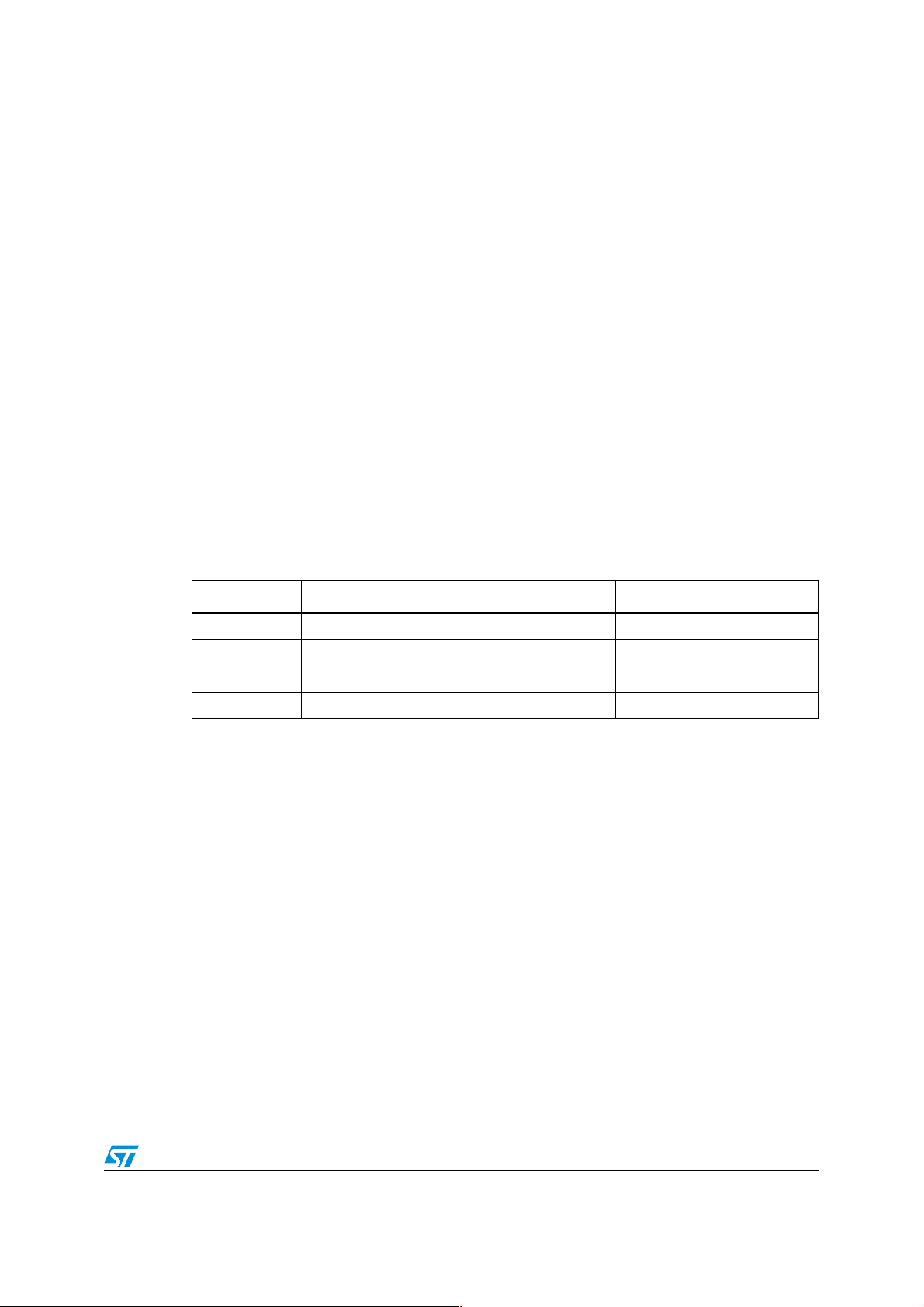
1.5 EBC maximum addressable space
The CSSELx (PH0.1 and P0H.2) field sampled at the end of a hardware reset controls the
active number of CSx signals.
The SALSELx (P0H.3 and P0H.4) field sampled at the end of a hardware reset selects the
number of address lines addressing an external location. It determines the size of the
maximum addressable space per chip select CSx. The following table gives the different
configurations.
Table 2.
P0H.3/P0H.4 Maximum EBC addressable space per CS Address lines used
ST10 EBC addressable space
01 64 Kbytes A0 .. A15 ( P1)
11 256 KBytes A0 .. A17 ( P1 , P4.0 & P4.1)
00 1 MByte A0 .. A19 ( P1, P4.0 .. P4.3)
10 16 MBytes A0 .. A23( P1 & P4)
Each CS1 … CS4 has its related ADDRSELx register to map the external memory within
the ST10 memory space. This register configures the size of the window allocated to the
external memory and its start address.
Note: The size specified in this register should not exceed the one specified by the SALSELx field.
For more details, please refer to the ST10 user manual.
CS0 can write to/read from any memory location outside the windows allocated to the
remaining CSx signals with respect to the maximum addressable space.
5/14
Page 6

EBC overview AN2164
The following figure gives an example of a ST10 interfaced with two memories using CS1
and CS2 (CSSEL = 00 so CS0
, CS1, CS2 are active; SALSEL = 11 allowing 256 Kbytes of
addressable space))
0x21FFFF
0x200000
0x10DDDD
0x100000
0x000000
128 KB memory
128 KB memory
connected to CS2
connected to CS2
ADDRSEL2 = 0x2005
ADDRSEL2 = 0x2005
64 KB memory
connected to CS1
ADDRSEL1 = 0x1004
The EBC maximum addressable space is therefore function of the two parameters SALSEL
and CSSEL.
The 16 MBytes can be either allocated to one external resource or divided into several
external memories and peripherals.
In the eventuality that one or both embedded CAN controllers are required by the
application, the port P4 lines become the input/output lines of these peripherals. This
reduces the maximum addressable space to 1Mbyte per chip select. By exploring the ST10
5 chip selects, up to 5 Mbytes can be accessed (1 Mbyte per chip select).
The following sections give some configurations of the ST10 external bus interfaced with
different memories.
6/14
Page 7

AN2164 How to connect an external memory to the ST10 with a demultiplexed bus
2 How to connect an external memory to the ST10 with
a demultiplexed bus
With a demultiplexed bus, the address lines are output on PORT1 and PORT4, and data are
input and output on PORT0.
When using the demultiplexed mode, the ST10 EBC control signals interface directly with
the external memory.
2.1 16-bit demultiplexed bus and word-wide memory example
This example interfaces the ST10 EBC with the M29F400BB (256Kb x 16) flash memory
produced by STMicroelectronics.
An addressable space of 256K means that 18-bit address lines (2
that in 16-bit mode, only even addresses are generated by the ST10 ( P1L.0 = 0 in this
mode). Therefore, P1 will output the 15 first address bits ( P1L.. P1L.7 & P1H0..P1H.7):
P1L.1 is connected to the memory A0 address line, P1L.2 is connected the memory A1
address line and so on.
The P4 will output the remaining address lines: P4.0 is connected to the memory address
line A15, P4.1 is connected to the memory address line A16 and P4.2 is connected to A17.
18
= 256K) are used. Note
Data is Input and Output on P0. The M29F400BB Chip Enable signal (E) is connected to a
ST10F27x chip select signal for example CS0.
Figure 1. ST10 interfaced with M29F400B Flash
W
A17
A16
A15
A14
A13
A12
A11
A10
A9
A8
A7
A6
A5
A4
A3
A2
A1
A0
E
R
D15
D14
D13
D12
D11
D10
D9
D8
D7
D.6
D5
D4
D3
D2
D1
D0
M29F400BB
5V
256K x16 bit
BYTE
R/B
RP
ST10
P4.2\A18
P4.1\A17
P4.0\A16
P1H.7\A15
P1H.6\A14
P1H.5\A13
P1H.4\A12
P1H.3\A11
P1H.2\A10
P1H.1\A9
P1H.0\A8
P1L.7\A7
P1L.6\A6
P1L.5\A5
P1L.4\A4
P1L.3\A3
P1L.2\A2
P1L.1\A1
P1L..0\A0
P0H.7\D15
P0H.6\D14
P0L.6\D13
P0H.4\D12
P0H.3\D11
P0H.2\D10
P0H.1\D9
P0H.0\D8
P0L.7\D7
P0L.6\D6
P0L.5\D5
P0L.4\D4
P0L.3\D3
P0L.2\D2
P0L.1\D1
P0L..0\D0
CSx
RD
WR
7/14
Page 8

How to connect an external memory to the ST10 with a demultiplexed bus AN2164
2.2 16-bit demultiplexed bus and byte-wide memories example
In this section, the ST10 is interfaced with two byte-wide memories M68F031A (32Kx8- bit)
produced by STMicroelectronics. Two configurations are proposed.
In the first configuration, by setting bit WRGCFG in SYSCON register, BHE (Byte High
Enable) operates as write high byte signal, and WR operates as WRL write low byte signal.
The two memories are enabled together by the same ST10 chip select signal for example
CS0
. The two memories output enable signals G are connected to the RD pin of the ST10.
The first memory write enable pin W
memory write enable W
is connected to the ST10 WRL pin.
Figure 2. ST10 interfaced with 2 M68F031A SRAM configuration 1
is connecetd to the ST10 WRH and the second
M68F031A
P1H.7\A15
P1H.6\A14
P1H.5\A13
P1H.4\A12
P1H.3\A11
P1H.2\A10
P1H.1\A9
P1H.0\A8
P1L.7\A7
P1L.6\A6
P1L.5\A5
P1L.4\A4
P1L.3\A3
P1L.2\A2
P1L.1\A1
P0H.7\D15
P0H.6\D14
P0H.5\D13
P0H.4\D12
P0H.3\D11
P0H.2\D10
P0H.1\D9
P0H.0\D8
A14
A13
A12
A11
A10
A9
A8
A7
A6
A5
A4
A3
A2
A1
A0
D7
D6
D5
D4
D3
D2
D1
D0
E
G
W
M68F031A
P1H.7\A15
P1H.6\A14
P1H.5\A13
P1H.4\A12
P1H.3\A11
P1H.2\A10
P1H.1\A9
P1H.0\A8
P1L.7\A7
P1L.6\A6
P1L.5\A5
P1L.4\A4
P1L.3\A3
P1L.2\A2
P1L.1\A1
P1L..0\A0
P0L.7\D7
P0L.6\D6
P0L.5\D5
ST10
P0L.4\D4
P0L.3\D3
P0L.2\D2
P0L.1\D1
P0L.0\D0
CSx
RD
WRL
WRH
A14
A13
A12
A11
A10
A9
A8
A7
A6
A5
A4
A3
A2
A1
A0
E
G
W
D7
D6
D5
D4
D3
D2
D1
D0
Note: This configuration can be used to interface the ST10 with a 16-bit memory which has one
chip enable signal CS and two write enable signals (Low Byte Write Enable and High Byte
Write Enable).
/* Defines */
#define BaseAddress 0x100000;
#define M68_High 0x000001;
#define M68_Low 0x000000;
/* Select CS1 for these two memories */
/* CS1 window mapping: Start address = 0x100000, size = 32Kbytes */
ADDRSEL 1 = 0x1003;
/* 16-bit de- multiplexed mode, with R/D delay, 1 waitstate, BSUCAT active */
BUSCON1 = 0x48E;
8/14
Page 9

AN2164 How to connect an external memory to the ST10 with a demultiplexed bus
The execution of the instruction:
* (huge unsigned char *) ((BaseAddress + MemOffset << 2) | M68_ID) =
byte
● outputs the byte data on both high and low bytes of the ST10 data lines
● activates the ST10 WRH if M68_ID equals the M68_High and ST10 WRL if the M68_ID
is M68_Low
● The byte is written into the address MemOffset of the selected memory.
For example, the execution of the instruction:
* (huge unsigned char *) 0x100023 = 0x55
● outputs the word 0x5555 on the data lines
● activates the ST10 WRH signal
● writes the 0x55 data byte in the address 0x0011 of the M68_High.
In the second configuration, by clearing bit WRGCFG in SYSCON register, BHE keeps its
function of Byte High Enable.
The first memory is enabled by the BHE signal and the second is selected by the ST10 A0
signal ( P1L.0) as this bit is equal to 0 in 16 demultiplexed bus. Therefore, the 2 memories
can be selected independently or together when word accesses are made.
Both memory output enable pins G
Both memory write enable W
are connected to the RD pin of the ST10.
pins are connected to the WR pin of the ST10.
Figure 3. ST10 interfaced with 2 M68F031A SRAM configuration 2
P1H.7\A15
P1H.6\A14
P1H.5\A13
P1H.4\A12
P1H.3\A11
P1H.2\A10
P1H.1\A9
P1H.0\A8
P1L.7\A7
P1L.6\A6
P1L.5\A5
P1L.4\A4
P1L.3\A3
P1L.2\A2
P1L.1\A1
P1L..0\A0
P0L.7\D7
P0L.6\D6
P0L.5\D5
ST10
P0L.4\D4
P0L.3\D3
P0L.2\D2
P0L.1\D1
P0L.0\D0
A14
A13
A12
A11
A10
A9
A8
A7
A6
A5
A4
A3
A2
A1
A0
E
G
W
D7
D6
D5
D4
D3
D2
D1
D0
P1H.7\A15
P1H.6\A14
P1H.5\A13
P1H.4\A12
P1H.3\A11
P1H.2\A10
P1H.1\A9
P1H.0\A8
P1L.7\A7
P1L.6\A6
P1L.5\A5
P1L.4\A4
P1L.3\A3
P1L.2\A2
P1L.1\A1
M68F031A
P0H.7\D15
P0H.6\D14
P0H.5\D13
P0H.4\D12
P0H.3\D11
P0H.2\D10
P0H.1\D9
P0H.0\D8
A14
A13
A12
A11
A10
A9
A8
A7
A6
A5
A4
A3
A2
A1
A0
D7
D6
D5
D4
D3
D2
D1
D0
E
G
W
M68F031A
BHE
RD
WR
Note: This configuration can be used to interface the ST10 with a 16-bit memory which has two
CS input signals (one for the low byte and one the high byte) and one signal WR.
9/14
Page 10

How to connect an external memory to the ST10 with a demultiplexed bus AN2164
The execution of the instruction:
* (huge unsigned char *) ((BaseAddress + MemOffset << 2) | M68_ID) =
byte
● outputs the byte data on both high and low bytes of the ST10 data lines
● activates the ST10 WR signals independently of the M68 memory
● activates the ST10 BHE if the M68_High is selected i.e. if (BaseAddress + MemOffset
<< 2) | M68_ID) is odd. In the other case, A0 = 0 selects the M68_Low memory.
● The byte is written into the address MemOffset of the selected memory.
In this configuration, the instruction:
* (huge unsigned char *) (0x100023) = 0x55
● outputs the word 0x5555 on the data lines
● activates both ST10 BHE and WR signals.
● The byte 0x55 is written in the address 0x0011 of the M68_High.
10/14
Page 11

AN2164 How to connect an external memory to the ST10 with a multiplexed bus
3 How to connect an external memory to the ST10 with
a multiplexed bus
With multiplexed bus modes, addresses are output on P0 and P4, and data is Input/Output
on P0.
As P0 is used for both data and addresses, the application must be able to latch the address
signals. The ALE signal (Address Latch Enable) purpose is to synchronize those latches
with the EBC address/data timing. Some memory devices embed the latches to simplify the
application’s layout. For more details regarding the ST10 multiplexed bus modes, refer to the
ST10 user manual.
3.1 16-bit multiplexed bus and word-wide memory example
In this section, the ST10, using the 16-bit multiplexed bus EBC mode, is interfaced with a
word-wide ST flash M29F200BB.
An addressable space of 128K means that 17-bit address lines (2
that in 16-bit mode, only even addresses are generated by the ST10F27x ( P1L.0 = 0 in this
mode). Therefore, P0 will output the 15 first address bits (P0L.1.. P0L.7 & P0H.0..P0H.7):
P0L.1 is connected to the memory A0 address line, P0L.2 is connected the memory A1
address line and so on.
17
= 128K) are used. Note
The P4 will ouput the remaining address lines: P4.0 is connected to the memory address
line A15 and P4.1 is connected to the memory address line A16.
Data is Input and Output on P0. The M29F400BB Chip Enable signal (E) is connected to a
ST10 chip select signal for example CS0.
Figure 4. ST10 interfaced with M29F400BB with a multiplexed bus
P4.1\A17
P4.0\A16
P0H.7\AD15
P0H.0\AD8
P0L.7\AD7
P0L.1\AD1
P0L.0\AD0
ST10
RD
W
ALE
Address
Latch
A16
A15
A14
A7
A6
A0
D15
D0
BYTE\
M29F200BB
ECSx
R
W
5V
11/14
Page 12

How to connect an external memory to the ST10 with a multiplexed bus AN2164
3.2 16-bit multiplexed and byte-wide memories example
In this section, the ST10 configured with a 16-bit multiplexed bus is interfaced with two bytewide memories M68F031A 32Kx8- bit produced by STMicroelectronics.
By setting bit WRGCFG in SYSCON register, BHE (Byte High Enable) operates as write
high byte signal, and WR operates as WRL write low byte signal.
The two memories are enabled together by the same ST10 chip select signal for example
CS0
. The two memories output enable signals G are connected to the RD pin of the ST10.
The first memory write enable pin W
memory write enable W
is connected to the ST10 WRL pin.
Figure 5. ST10 with a 16-bit-multiplxed bus interfaced with 2 M68F031A SRAM
is connected to the ST10 WRH and the second
P1H.7\AD15
P1H.0\AD8
P1L.7\AD7
P1L.1\AD1
P1L.0\AD0
ST10
ALE
RD
WRL
WRH
Address
Latch
A14
A7
A6
A0
D7
D0
M68F031A
ECSx
G G
W
D7
D0
A14
A7
A6
A0
M68F031A
E
W
12/14
Page 13

AN2164 Revision history
4 Revision history
Table 3. Document revision history
Date Revision Changes
31-May-2007 1 Initial release.
13/14
Page 14

AN2164
Please Read Carefully:
Information in this document is provided solely in connection with ST products. STMicroelectronics NV and its subsidiaries (“ST”) reserve the
right to make changes, corrections, modifications or improvements, to this document, and the products and services described herein at any
time, without notice.
All ST products are sold pursuant to ST’s terms and conditions of sale.
Purchasers are solely responsible for the choice, selection and use of the ST products and services described herein, and ST assumes no
liability whatsoever relating to the choice, selection or use of the ST products and services described herein.
No license, express or implied, by estoppel or otherwise, to any intellectual property rights is granted under this document. If any part of this
document refers to any third party products or services it shall not be deemed a license grant by ST for the use of such third party products
or services, or any intellectual property contained therein or considered as a warranty covering the use in any manner whatsoever of such
third party products or services or any intellectual property contained therein.
UNLESS OTHERWISE SET FORTH IN ST’S TERMS AND CONDITIONS OF SALE ST DISCLAIMS ANY EXPRESS OR IMPLIED
WARRANTY WITH RESPECT TO THE USE AND/OR SALE OF ST PRODUCTS INCLUDING WITHOUT LIMITATION IMPLIED
WARRANTIES OF MERCHANTABILITY, FITNESS FOR A PARTICULAR PURPOSE (AND THEIR EQUIVALENTS UNDER THE LAWS
OF ANY JURISDICTION), OR INFRINGEMENT OF ANY PATENT, COPYRIGHT OR OTHER INTELLECTUAL PROPERTY RIGHT.
UNLESS EXPRESSLY APPROVED IN WRITING BY AN AUTHORIZED ST REPRESENTATIVE, ST PRODUCTS ARE NOT
RECOMMENDED, AUTHORIZED OR WARRANTED FOR USE IN MILITARY, AIR CRAFT, SPACE, LIFE SAVING, OR LIFE SUSTAINING
APPLICATIONS, NOR IN PRODUCTS OR SYSTEMS WHERE FAILURE OR MALFUNCTION MAY RESULT IN PERSONAL INJURY,
DEATH, OR SEVERE PROPERTY OR ENVIRONMENTAL DAMAGE. ST PRODUCTS WHICH ARE NOT SPECIFIED AS "AUTOMOTIVE
GRADE" MAY ONLY BE USED IN AUTOMOTIVE APPLICATIONS AT USER’S OWN RISK.
Resale of ST products with provisions different from the statements and/or technical features set forth in this document shall immediately void
any warranty granted by ST for the ST product or service described herein and shall not create or extend in any manner whatsoever, any
liability of ST.
ST and the ST logo are trademarks or registered trademarks of ST in various countries.
Information in this document supersedes and replaces all information previously supplied.
The ST logo is a registered trademark of STMicroelectronics. All other names are the property of their respective owners.
© 2007 STMicroelectronics - All rights reserved
STMicroelectronics group of companies
Australia - Belgium - Brazil - Canada - China - Czech Republic - Finland - France - Germany - Hong Kong - India - Israel - Italy - Japan -
Malaysia - Malta - Morocco - Singapore - Spain - Sweden - Switzerland - United Kingdom - United States of America
www.st.com
14/14
 Loading...