

Page 1

AN2156
APPLICATION NOTE
STR73x Family
STR73x Hardware Getting Started
Introduction
The aim of this application note is to give users of the STR73x family devices a number of
recommendations on the HW circuitry connected to the main special pins. It covers the pins for power
supply (digital and analog), reset, crystal oscillator, the decoupling of the internal voltage regulator, boot
modes, test pin, RC oscillator biasing pin and the JTAG debug port.
Detailed reference design schematics of the STR730-EVAL board are also contained in this document
with descriptions of the main components, interfaces and modes.
Rev 1
September 2005 1/24
24
Page 2

- AN2156
Contents
1 Power management . . . . . . . . . . . . . . . . . . . . . . . . . . . . . . . . . . . . . . . . . . . . 4
1.1 Power supply pins VDD/VSS . . . . . . . . . . . . . . . . . . . . . . . . . . . . . . . . . . . . . 4
1.2 Analog supply and reference VDDA/VSSA . . . . . . . . . . . . . . . . . . . . . . . . . . . 4
1.3 Decoupling of the internal voltage regulator V18 . . . . . . . . . . . . . . . . . . . . . . 5
2 Clock management . . . . . . . . . . . . . . . . . . . . . . . . . . . . . . . . . . . . . . . . . . . . 7
2.1 Crystal oscillator pins XTAL1, XTAL2 . . . . . . . . . . . . . . . . . . . . . . . . . . . . . . . 7
2.2 On-chip RC oscillator and VBias pin . . . . . . . . . . . . . . . . . . . . . . . . . . . . . . . . 7
3 Reset management . . . . . . . . . . . . . . . . . . . . . . . . . . . . . . . . . . . . . . . . . . . . 8
3.1 Reset pin nReset . . . . . . . . . . . . . . . . . . . . . . . . . . . . . . . . . . . . . . . . . . . . . . 8
4 Boot management . . . . . . . . . . . . . . . . . . . . . . . . . . . . . . . . . . . . . . . . . . . . . 9
4.1 SystemMemory / User Boot mode pins M0, M1 . . . . . . . . . . . . . . . . . . . . . . . 9
4.2 Test mode . . . . . . . . . . . . . . . . . . . . . . . . . . . . . . . . . . . . . . . . . . . . . . . . . . . 11
5 Debug management . . . . . . . . . . . . . . . . . . . . . . . . . . . . . . . . . . . . . . . . . . 12
5.1 JTAG debug port pins . . . . . . . . . . . . . . . . . . . . . . . . . . . . . . . . . . . . . . . . . . 12
6 Reference design . . . . . . . . . . . . . . . . . . . . . . . . . . . . . . . . . . . . . . . . . . . . . 15
6.1 Main . . . . . . . . . . . . . . . . . . . . . . . . . . . . . . . . . . . . . . . . . . . . . . . . . . . . . . . 15
6.2 Clock . . . . . . . . . . . . . . . . . . . . . . . . . . . . . . . . . . . . . . . . . . . . . . . . . . . . . . . 15
6.3 Reset . . . . . . . . . . . . . . . . . . . . . . . . . . . . . . . . . . . . . . . . . . . . . . . . . . . . . . . 15
6.4 Boot mode . . . . . . . . . . . . . . . . . . . . . . . . . . . . . . . . . . . . . . . . . . . . . . . . . . . 15
6.5 Wake-Up . . . . . . . . . . . . . . . . . . . . . . . . . . . . . . . . . . . . . . . . . . . . . . . . . . . . 15
6.6 Power supplies . . . . . . . . . . . . . . . . . . . . . . . . . . . . . . . . . . . . . . . . . . . . . . . 15
6.7 CAN interface . . . . . . . . . . . . . . . . . . . . . . . . . . . . . . . . . . . . . . . . . . . . . . . . 16
6.8 RS232 serial interface . . . . . . . . . . . . . . . . . . . . . . . . . . . . . . . . . . . . . . . . . . 16
6.9 Serial ROM . . . . . . . . . . . . . . . . . . . . . . . . . . . . . . . . . . . . . . . . . . . . . . . . . . 16
6.10 JTAG interface . . . . . . . . . . . . . . . . . . . . . . . . . . . . . . . . . . . . . . . . . . . . . . . . 16
7 Schematics . . . . . . . . . . . . . . . . . . . . . . . . . . . . . . . . . . . . . . . . . . . . . . . . . 17
2/24
Page 3

AN2156 -
8 Revision history . . . . . . . . . . . . . . . . . . . . . . . . . . . . . . . . . . . . . . . . . . . . . . 23
3/24
Page 4
1 - Power management AN2156
1 Power management
1.1 Power supply pins VDD/VSS
All current STR73x devices are supplied with a nominal voltage of 5V. The power supply pins
are organized in VDD/VSS pairs around the chip and exceptionally all pins need to be properly
connected to the power supplies, VDD to 5V, VSS to GND. These connections including pads,
tracks and vias should have an impedance as low as possible. This is typically achieved with
thick track widths and preferably dedicated power supply planes in multi layer PCBs.
In addition, each VDD/VSS pair should be decoupled with ceramic capacitors which need to be
placed as close as possible to the appropriate pins or below the pins on the contrary side of the
PCB. Typical values are 10nF to 100nF, but exact values depend on the application needs. The
following figure shows the typical layout on such a VDD/VSS pair.
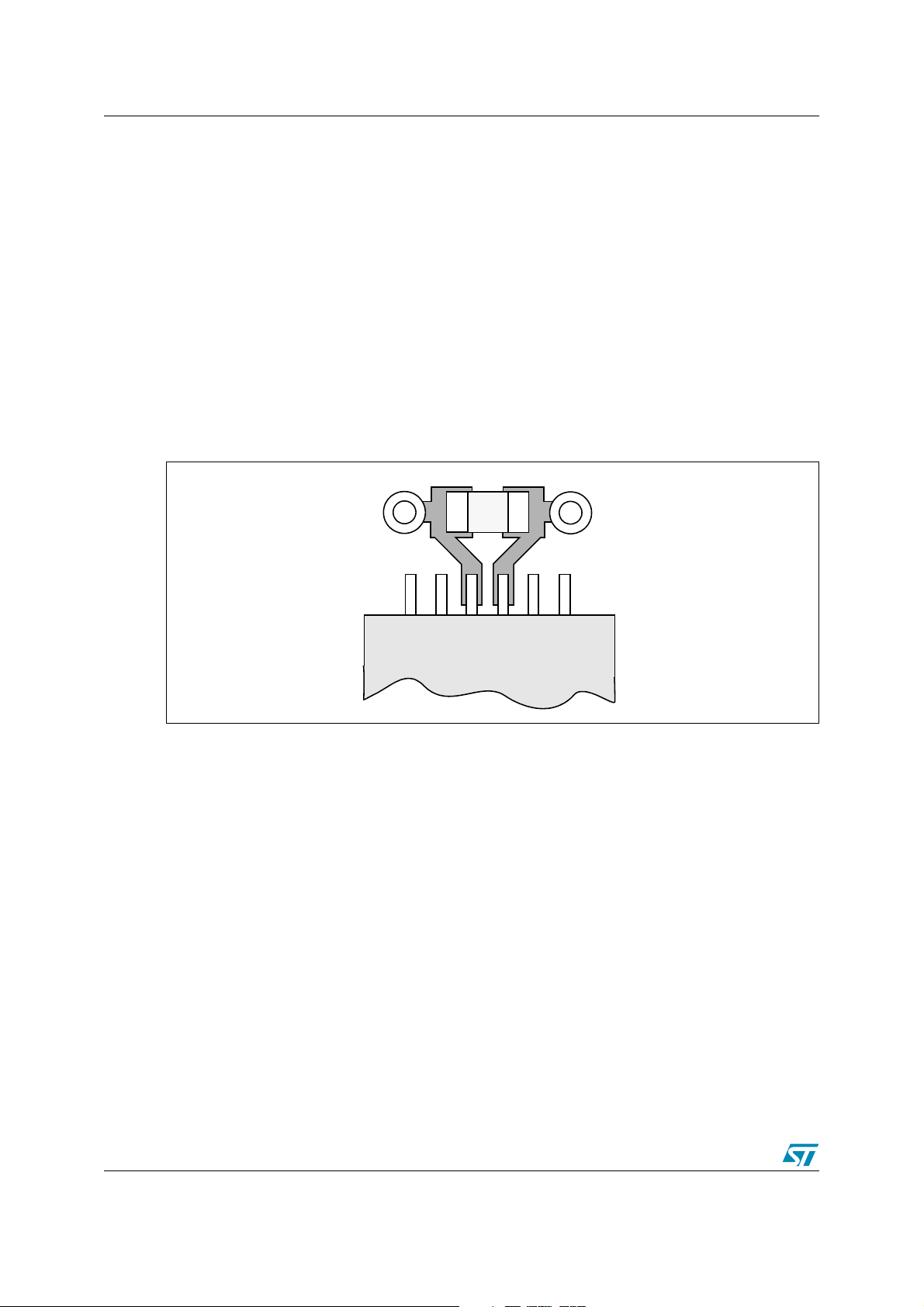
Figure 1. Typical layout for VDD/VSS pair
Via to VSSVia to VDD
Cap.
V
DDVSS
STR73x
1.2 Analog supply and reference V
The V
As for the supply pins, V
X7R ceramic capacitor of 47nF to 100nF can be used for this.
When full accuracy is needed, and depending on the noise rejection of the voltage regulator
used to supply the STR73x device, a low pass filter may be considered. As the pin is also used
as the ADC supply, the use of a serial resistor must be avoided to reduce the risk of offset error
generation. An EMI component from Murata is proposed instead.
pin is used to supply the ADC and to provide it with the analog reference.
DDA
DDA/VSSA
decoupling with short connections is recommended and an
DDA/VSSA
4/24
Page 5
AN2156 1 - Power management
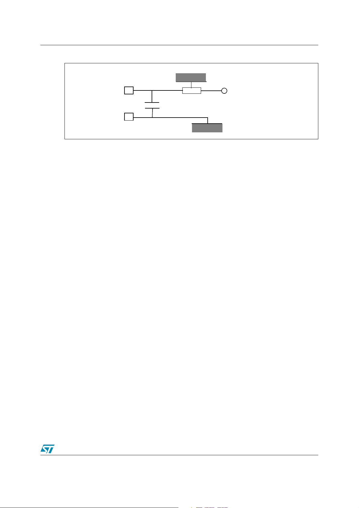
Figure 2. V
DDA/VSSA
V
decoupling with an X7R ceramic capacitor
DDA
+5V
U1
V
C1
SSA
C1 = 47 to 100nF X7R ceramic capacitor
U1 = Murata NFM18PC105R0J3 – 1uF
1.3 Decoupling of the internal voltage regulator V18
All existing STR73x derivates are supplied with a single external voltage of 5V. The additional
voltages needed are generated by internal charge pump circuits for the flash programming/
erasing and an internal linear voltage regulator which provides the 1.8V for the internal logic.
The output of the internal voltage regulator is connected to one or two pins V18, where an
external capacitance needs to be connected for decoupling/stabilization between the V18 pin
and VSS/GND. There are two important notes:
1. V18 is probably the most critical pin regarding EMC emissions. Therefore the external
capacitor(s) must be placed as close as possible (few mm) to the V18/VSS pair(s) or
below on the other side of the PCB. If this is done, a very good EMC performance can be
achieved.
2. Depending on the device, different capacitances are needed. The values mainly depend
on the type of the internal voltage regulator used. Please refer to the tables below which
cover the devices available or planned at the time of writing. In case of future devices
which are not covered by this application note please refer to the datasheet or contact your
support engineer.
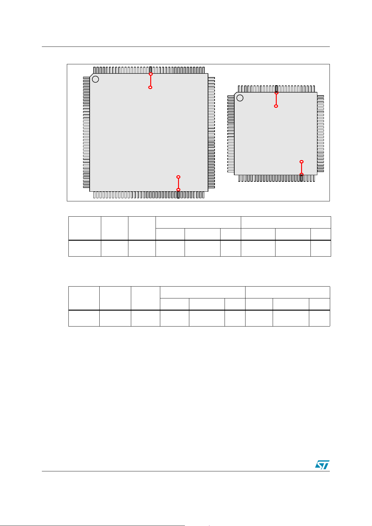
The figure below shows the two affected pins (V18 and VBias) of the TQFP144 package as well
as the TQFP100 package. In order to support all devices with a single PCB design, it is
necessary to provide on both pins footprints for 10µF tantalum and 47-100nF ceramic
capacitors. The footprint for the ceramic capacitor on pin 64 should be reusable to be soldered
with a resistor instead for the biasing functionality. This may be achieved with 0805 or 0603
SMD footprints. Please refer to the tables below for the different component values and
assembly options depending upon the device derivate.
5/24
Page 6
1 - Power management AN2156
Figure 3. Pin availability for V18 functionality
Pin 126 : V
18
TQFP144 Packages
Pin 64 : V
Bias
Table 1. Component values for TQFP144 package
Package Derivate
TQFP144/
LFBGA144
STR730
STR735
CMU /
RC osc.
yes VBias resistor (*) 1.3MΩ V18 ceramic cap 100nF
Function Component Value Function Component value
Pin 64 Pin 126
(*) only necessary for 32kHz mode of RC oscillator
Pin 88 : V
18
TQFP100 Packages
Pin 46 : V
Bias
Table 2. Component values for TQFP100 package
Package Derivate
TQFP100
STR731
STR736
CMU / RC
osc.
yes VBias resistor (*) 1.3MΩ V18 ceramic cap 100nF
Function Component Value Function Component value
Pin 46 Pin 88
(*) only necessary for 32kHz mode of RC oscillator
6/24
Page 7
AN2156 2 - Clock management
2 Clock management
2.1 Crystal oscillator pins XTAL1, XTAL2
All current STR73x devices have an on-chip oscillator that allows the driving of external crystals
or resonators with a fundamental frequency of 4-8 MHz. The recommended circuitry for a
crystal is shown below. C1, C2 and R1 values depend greatly on the crystal type and
manufacturer. It is suggested that you ask your crystal supplier for the best values for these
components.
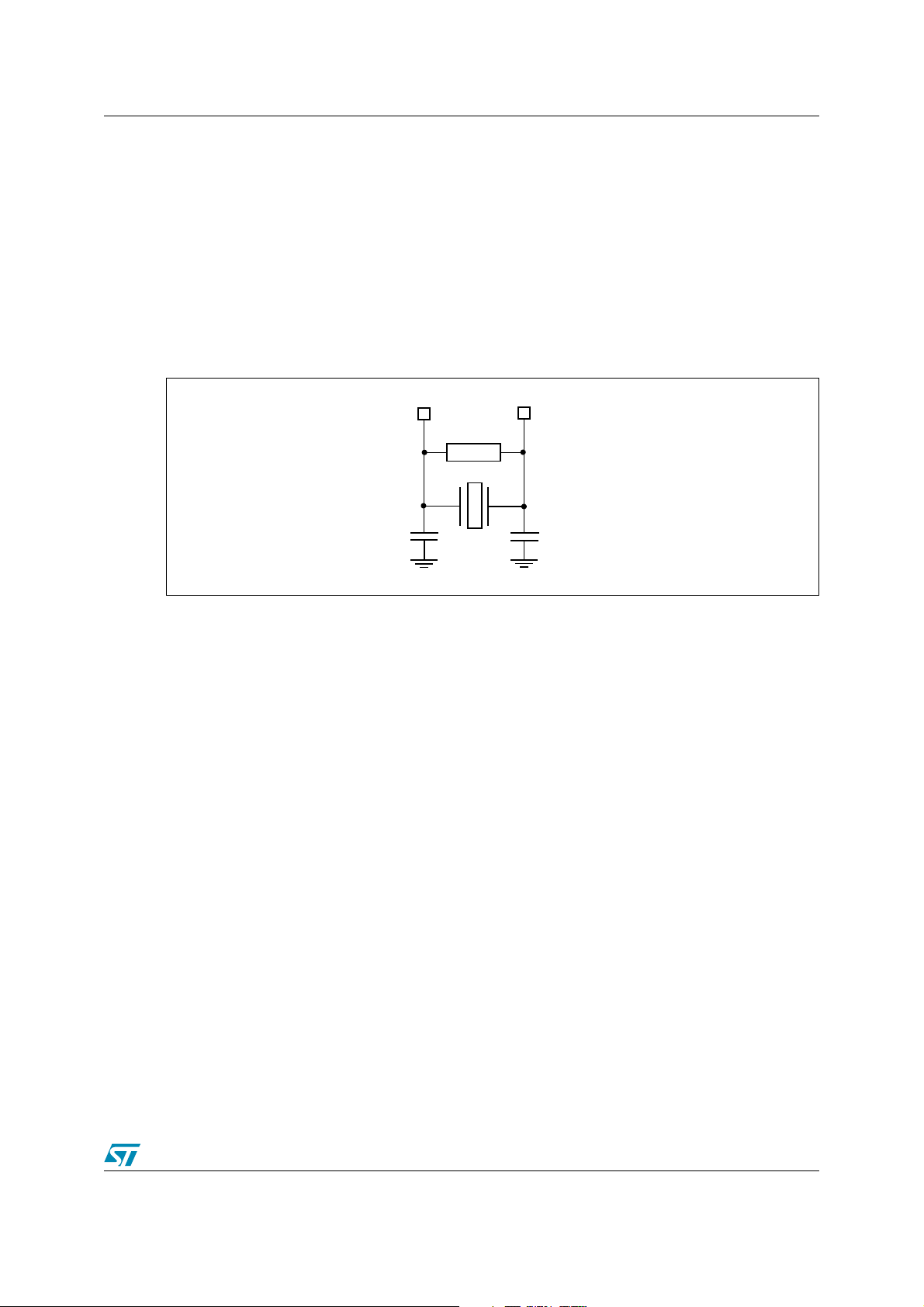
Figure 4. Recommended circuitry for crystal oscillator pins XTAL1 and XTAL2
XTAL1
Resistor R1 is recommended for feedback stability and has a value of around 1M
oscillator of STR73x devices has automatic gain control, there is no need to add a resistance in
series.
The values of the load capacitors C1 and C2 are also heavily dependent on the crystal type and
frequency. For best oscillation stability they normally have the same value. Typical values are in
the range from below 10pF up to 30pF. The parasitic capacitance of the board layout also
needs to be considered and typically adds a few pF to the component values.
In the PCB layout all connections should be as short as possible. Any additional signals,
especially those that could interfere with the oscillator, should be locally separated from the
PCB area around the oscillation circuit using suitable shielding.
XTAL2
R1
C2C1
Ω. As the
2.2 On-chip RC oscillator and VBias pin
All devices of the STR73x family have an on-chip RC oscillator in addition to the main oscillator.
This on-chip RC oscillator is capable of running at either 2MHz or 32kHz.
● The default 2MHz mode requires no external components.
● The 32 kHz mode requires an external bias resistor of 1.3 MΩ from the VBias pin towards
GND.
Note: The oscillator frequencies can be adjusted through software after reset, where the reset
frequencies are around 2.34Mhz / 29Khz.
7/24
Page 8
3 - Reset management AN2156
3 Reset management
3.1 Reset pin nReset
All current STR73x devices are specified for a nominal voltage of 5V with a tolerance of ±10%,
thus between 4.5V and 5.5V. The external reset circuitry should apply a reset whenever the
supply voltage is outside this voltage supply range and only release it when inside the supply
range.
Being within the supply range of 5V ±10%, the absolute minimum duration of the hardware
reset pulse is 100µs, but it is recommended that the reset circuitry adds increased time margin,
e.g. 200µs.
Note: During power-on, a reset must be provided externally.
At power-on, the nRSTIN pin must be held low by an external reset circuit until V
is reached.
DD
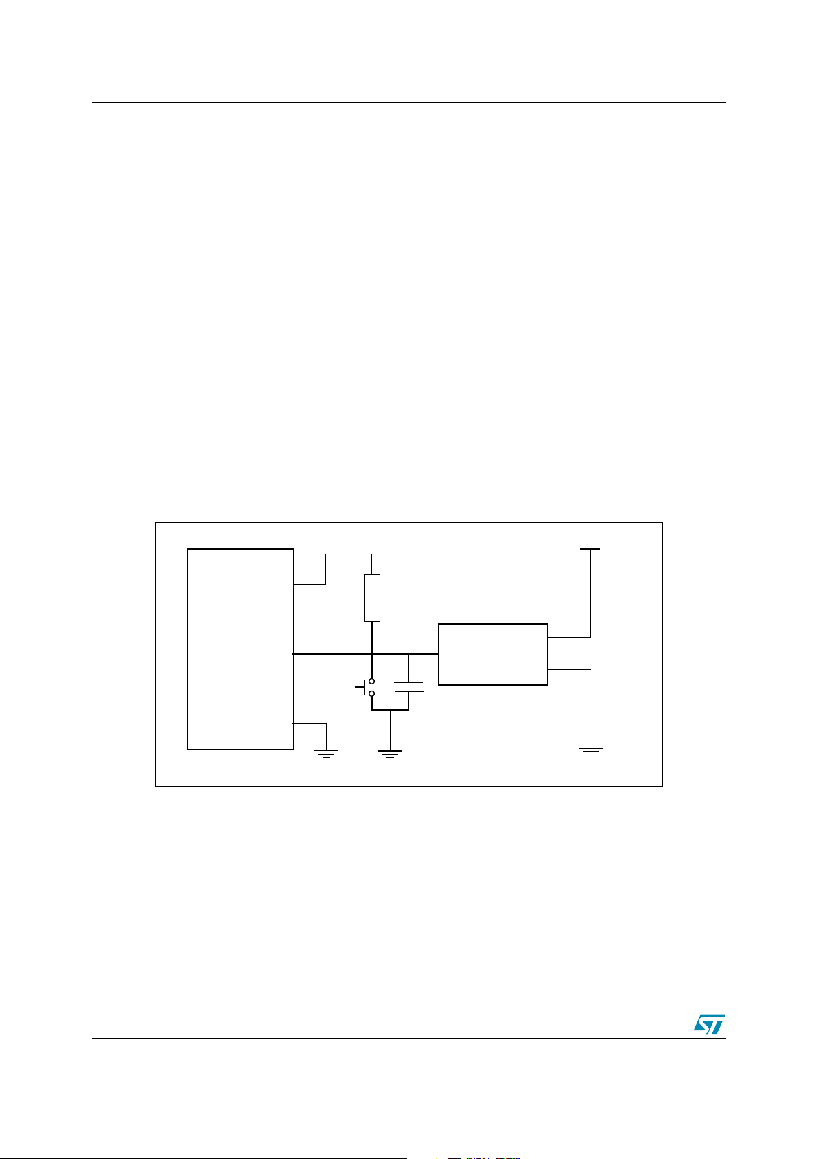
Figure 5 gives an example of the hardware implementation of the RESET circuit for STR73x
devices.
The STM1001 low-power CMOS microprocessor supervisory circuit is used to assert a reset
signal whenever the V
voltage falls below a preset threshold or whenever a manual reset is
DD
asserted.
Figure 5. Hardware reset implementation
+5V +5V
V
DD
2K2*
+5V
2
VCC
GND
3
nRSTIN
V
Reset_PB
SS
* these values are given only as typical examples
1nF*
1
not Reset
8/24
Page 9

AN2156 4 - Boot management
4 Boot management
4.1 SystemMemory / User Boot mode pins M0, M1
The recommended circuitry around the mode pins M0 and M1 depends upon the end of line
programming strategy for virgin devices. The device always operates (i.e. executes the
application) in user boot mode and it is also possible to program the device via the JTAG debug
port in this mode. Field updates, where the application is already running and updating itself,
also use this mode. Depending solely on the application, any interface may be used for field
updates such as CAN or UART.
The support of SystemMemory boot mode is necessary only when virgin devices or
applications which are not able to update themselves, are programmed via CAN or UART.
Please note that circuitry is needed that supports both user and SystemMemory boot modes.
ST prefers programming via the JTAG port, since it provides the fastest possible method, no
interface resources are necessary, the handling is easier and a lot of professional end-of-line
programming solutions already exist from well known companies such as PLS and BP
Microsystems.
4.1.1 End of line programming via JTAG
If you know already that you will program the devices only via the JTAG debug port, simply
connect both mode pins M0 and M1 directly or via pull-down resistors to GND.
Figure 6. M0 and M1 pin connections
M0 M1
4.1.2 End of line programming via UART or CAN
If you are not yet sure which end of line programming method to use or you know that you will
use the SystemMemory boot mode method, you need dynamic handling of the mode pins.
The voltage levels on the mode pins are latched with a rising edge on the reset pin. When both
M0 and M1 are low at this time then user boot mode is entered. When M0 is low and M1 high at
this time then SystemMemory boot mode is entered and the testflash sector is aliased at
address 0 instead of the normal sector 0.
As long as M1 stays high the clock is stretched and no code is executed. So in order to run the
bootstraploader code of the testflash sector a falling edge on M1 is needed some time after the
rising edge on reset. This time is not critical but must exceed 500ns. The following figure shows
the timing.
9/24
Page 10

4 - Boot management AN2156
Figure 7. Timing diagram for RSTIN, M0 and M1
RSTIN
M0
M1
SystemMemory
Latching of M0 and M1
Boot mode with support of external HW such as a Tester
>500ns
The easiest way to support the SystemMemory boot mode without adding much complexity
and cost is to replace the direct connection of M0 and M1 pins towards GND with pull-down
resistors and to add one test pin each directly connected to M0 and M1. The pull-down
resistors should have a value of around 10k
Ω. If no further hardware is connected to the
testpins the user boot mode will be selected. If however a tester provides the necessary
dynamic voltages to the testpins via a needle adaptor the SystemMemory bootmode can be
used.
Figure 8. M1 and M0 connections giving support for external tester
M0M1
R2 R1
SystemMemory
Boot mode with onboard circuitry
The necessary dynamic signals can also be generated by onboard circuitry so that no external
hardware is necessary. The following schematic shows how this could be done. During active
reset (nRSTIN low) the transistor is in high impedance and the capacitor is uncharged through
the two resistors R1, resulting in M1 being high. As soon as the reset signal is deasserted high
the transistor switches to low impedance after the charge of the capacitor via resistor R1 and
R3.(when the Vbe of the transistor is upper than 0.7V). As a consequence M0 will become low
after a period of a few µs.
10/24
TestpointTe s tp o i n t
Page 11

AN2156 4 - Boot management
Figure 9. SystemMemory Boot mode development circuitry example
V
CC
V
CC
2
1
SW0: 1-3 & SW1:1-3 User Boot Mode 1
SW0: 2-3 & SW1:1-3 User Boot Mode 2
SW0: 1-3 & SW1:2-3 SystemMemory Boot Mode
SW0: 2-3 & SW1:2-3 Reserved
4.2 Test mode
The TST pin must always be connected to GND to disable testmode. Testmode is ST’s
reserved mode and must never be used by the application.
Figure 10. TST pin connection
SW0
M0
M1
R3
10K
SW1
3
3
2
1
R1
nRSTIN
47k
C1
T1, e.g.BC847
2.2nF
TST
11/24
Page 12

5 - Debug management AN2156
5 Debug management
5.1 JTAG debug port pins
The JTAG interface is a special synchronous serial port and provides access to the internal
scanchains and the debug logic. Some of these scanchains are around the ARM core and the
Embedded ICE Unit. With these it is possible to insert data into and read from the processor’s
pipeline, to program breakpoints and watchpoints and to control the debugging.
Since the JTAG port is an integral part of the ARM core it is available on every device and thus
also allows in-system debugging and in-system flash-programming directly in the target
application. The JTAG interface pins consist of the following signals:
Table 3. JTAG interface signals
Std name STR73x name Direction/Description Function
This active LOW open-collector is used to
reset the JTAG port and the associated
debug circuitry. It is asserted at power-up by
each module, and can be driven by the JTAG
equipment.
TDI goes down the stack of modules to the
motherboard and then back up the stack,
labelled TDO, connecting to each
component in the scan chain.
TMS controls transitions in the tap controller
state machine. TMS connects to all JTAG
components in the scan chain as the signal
flows down the module stack.
TCK synchronizes all JTAG transactions.
TCK connects to all JTAG components in the
scan chain. Series termination resistors are
used to reduce reflections and maintain
good signal integrity. TCK flows down the
stack of modules and connects to each
JTAG component. However, if there is a
device in the scan chain that synchronizes
TCK to some other clock, then all downstream devices are connected to the RTCK
signal on that component.
Some devices sample TCK (for example a
synthesizable core with only one clock), and
this has the effect of delaying the time that a
component actually captures data. Using a
mechanism called adaptive clocking, the
RTCK signal is returned by the core to the
JTAG equipment, and the clock is not
advanced until the core had captured the
data. In adaptive clocking mode, the
debugging equipment waits for an edge on
RTCK before changing TCK.
nTRST JTRST
TDI JTDI
TMS JTMS
TCK JTCK
RTCK
GND
(not used)
Test Reset (from JTAG
equipment)
Test data in (from JTAG
equipment)
Test mode select (from
JTAG equipment)
Test clock (from JTAG
equipment)
Return TCK (to JTAG
equipment)
12/24
Page 13

AN2156 5 - Debug management
Std name STR73x name Direction/Description Function
TDO JTDO
nSRST nRSTIN
DBGRQ
DBGACK
GND
(not used)
GND
(not used)
Test data out (to JTAG
equipment)
System reset
(bidirectional)
Debug request (from
JTAG equipment)
Debug acknowledge (to
JTAG equipment)
The JTAG input signals have weak internal pull-up and pull-down resistors, but these are not
always active:
● When debug protection is activated (JTAG permanently held in reset internally)
● At power up and down there may be a short duration where the power on reset is already
released internally, but where the resistors are not yet active.
TDO is the return path of the data input
signal TDI.
nSRST is an active LOW open-collector
signal that can be driven by the JTAG
equipment to reset the target board. Some
JTAG equipment senses this line to
determine when a board has been reset by
the user.
When the signal is driven LOW by the reset
controller on the core module, the
motherboard resets the whole system by
driving nSYSRST low.
DBGRQ is a request for the processor core
to enter debug state.
DBGACK indicates to the debugger that the
processor core has entered debug mode.
To avoid any floating input pins even for a very short period it is highly recommended to always
provide additional external pull-up and pull-down resistors. This recommendation is valid
whether the JTAG port is used or not.
The following table shows the recommended values and types:
Table 4. Recommended JTAG debug port components
Signal name
JTCK
JTDI
JTDO Output, no resistor needed N.A.
JTMS
JTRST
Recommended external
Resistor type
Pull-down between pin and VSS/
GND
Pull-up between pin and VDD/
VCC
Pull-up between pin and VDD/
VCC
Pull-down (*) between pin and
VSS/GND
Recommended value
10kΩ
10kΩ
10kΩ
10kΩ
To connect the target with a debugger some additional signals are needed, mainly the System
Reset nRSTIN, so that the debugger can also reset the whole MCU, not only the JTAG part.
nRSTIN should be an open collector so that the different reset sources (power-on reset
circuitry, ext. watchdog if available and the JTAG equipment/Debugger) can be connected
together. The Debugger itself will also monitor the level on nRSTIN, so that it recognizes when
a reset is forced by some other circuitry.
Finally the target supply voltage must be provided so that the Debugger may adapt voltage
levels appropriately.
13/24
Page 14

5 - Debug management AN2156
All signals should be made accessible at least as testpoints that can then be fed via some
needle adaptors to the ARM standard JTAG connector. If cost and space allow, the connector
can also be directly put on the target PCB. The connector is a standard two row, 20-pin header
connector with a pitch of 0.1 inch / 2.54 mm and should have a collar to avoid incorrect
mounting.
14/24
Page 15

AN2156 6 - Reference design
6 Reference design
6.1 Main
The STR730-EVAL board is based on the STR730FZ2T7, a highly integrated microcontroller,
running at up to 36 MHz that uses the popular ARM7TDMI
chip high speed single voltage flash memory and high-speed RAM, clock generation via PLL,
and numerous on-chip peripherals.
6.2 Clock
Clocking is performed by a +5 V surface mounted 8 MHz quartz. Please refer to the
Section 2.1: Crystal oscillator pins XTAL1, XTAL2 for more details.
6.3 Reset
One push button SW_PB:S100 is used to generate a hardware reset. Please refer to the
Section 3: Reset management for more details.
6.4 Boot mode
The are three different modes available and can be enabled by means of two dedicated Input
only pins:
User Boot Mode 1: In this mode, Flash sector B0F0 is mapped in both Block 010 and Block
000 of the memory map. The system boots from block 0, segment 0 of Flash (normal operation)
TM
32-bit RISC CPU featuring on-
User Boot Mode 2: This mode has the same mapping as User Boot mode 1 except Flash
sector B0F1 is reserved and any attempt to access address range 0x8000 2000 to 0x8000
3FFF will generate an ABORT.
SystemMemory Boot mode: This mode has the same mapping as User Flash boot mode 1,
except that the SystemMemory flash sector is accessible in address range 0x8010 C000 to
0x8010 DFFF and is aliased in Block 0 This allows the system to boot from SystemMemory (for
initial Flash Programming).
Please refer to the Section 4: Boot management for more details.
6.5 Wake-Up
Push button S103 is connected to Wake-up line 16 and is used to exit from Stop mode.
For more details, please refer to the STR73x Reference Manual.
6.6 Power supplies
Power to the board is supplied using a lump in cord power supply providing 5 V to the board.
For more details, refer to Section 1: Power management.
15/24
Page 16

6 - Reference design AN2156
6.7 CAN interface
A general purpose, asynchronous serial I/O data port connected through a 9-pin D-type male
connector with micro switches selectable between High or Low bus output S702, and between
Standby or Slope control S50.
For more details, refer to the CAN transceiver L9616 datasheet.
6.8 RS232 serial interface
A general purpose, asynchronous serial I/O data port connected through a 9-pin D-type male
connector.
RS232 connects directly to UART0, transmit and receive only (null modem).
RTS is shorted to CTS and DTR is shorted to DSR at the connector.
For more details, refer to the RS232 transceiver ST3232 datasheet.
6.9 Serial ROM
6.9.1 SPI EEPROM
8 Kbit SPI serial EEPROM connected to the buffered serial peripheral interface (BSPI). Switch
S41 is used to enable or disable write protect (pull down = Write protect, pull up = Write
enabled).
For more details, refer to the SPI EEPROM M95080 datasheet.
6.9.2 I2C EEPROM:
8 Kbit EEPROM connected to the I2C0 interface, Switch S40 is used to enable or disable write
protect (pull down = Write protect, pull up = Write enabled).
For more details, refer to the I2C EEPROM M24C08 datasheet.
The values R43 and R45 depend essentially on the I2C communication speed.
For more details on theses values, please refer to the STR73x Reference Manual.
6.10 JTAG interface
Refer to the Section 5: Debug management.
16/24
Page 17

AN2156 7 - Schematics
7 Schematics
D
C
B
A
+5V
654321
MISO
MOSI
SCLK
SSN
not S
page 4
Serial_ROM.Sch
RX
TX
page 5
RS232.Sch
+5V
+5VAN
2
VCC
VSS
R106
2K2
U101
STM1001L (4.63V)
110
111
112
113
114
115
116
117
118
119
120
121
122
123
124
125
129
130
131
132
133
134
135
136
137
138
139
140
141
142
143
144
VDD
128
VDD
93
VDD
85
VDD
66
VDD
50
VDD
26
VDD
6
VDD
15
AVDD
76
U100
3
not RESET
1
C100
1nF
S100
SW-PB
1M3
R104
100
64
63
109
VBIAS
Reserved
MOSI1_P5.0
MISO1_P5.1
OCMPA9_P5.2
SCK1_WUP22_P4.15
OCMPB9_P5.3
not SS2_P5.4
SCK2_WUP23_P5.5
MOSI2_P5.6
MISO2_P5.7
INT6_P5.8
INT7_P5.9
RD12_INT8_P5.10
TD02_INT9_P5.11
INT10_P5.12
INT11_P5.13
INT12_P5.14
INT13_P5.15
WUP0_P6.0
WUP1_P6.1
RDI3_WUP2_P6.2
WUP3_P6.3
TDO3_WUP4_P6.4
WUP5_P6.5
WUP6_P6.6
WUP7_P6.7
RDI0_WUP10_P6.8
TDO0_P6.9
WUP8_P6.10
MISO0_P6.11
MOSI0_P6.12
SCK0_WUP11_P.13
notSS0_P6.14
WUP9_P6.15
OCMPA2_P0.1
ICAPA2_P0.2
OCMPB2_P0.0
2
3
1
101
105
106
107
108
104
103
102
99
SDA1_P4.7
ICAPB6_P4.9
not SS1_P4.14
ICAPB9_P4.13
OCMPA8_P4.8
OCMPB8_P4.11
SCL1_WUP19_P4.6
ICAPA6_WUP20_P4.10
ICAPA9_WUP21_P4.12
ICAPB2_P0.34OCMPA5_P0.47OCMPB5_P0.58ICAPA5_P0.69ICAPB5_P0.7
OCMPA6_P0.811OCMPB6_P0.912OCMPA7_P0.1013OCMPB7_P0.1114ICAPA3_P0.1217ICAPB3_P0.1318OCMPB3_P0.1419OCMPA3_P0.1520OCMPA4_P1.021OCMPB4_P1.122ICAPB4_P1.223ICAPA4_P1.324P1.427P1.528OCMPB1_P1.629OCMPA1_P1.730INT0_OCMPA0_P1.831INT1_OCMPB0_P1.932ICAPB0_WUP28_P1.1033ICAPA0_WUP29_P1.1134ICAPA1_WUP30_P1.1235ICAPB1_WUP31_P1.1336WUP12_CAN0RX_P1.1437CAN0TX_P1.15
10
JTAG.Sch
97
98
96
95
94
CAN2TX_P4.4
ICAPA8_WUP26_P4.2
ICAPA7_WUP24_P4.0
ICAPB8_WUP27_P4.3
ICAPB7_WUP25_P4.1
CAN2RX_WUP18_P4.5
R107
47K
10K
R108
+5V
+5V
SW SPDT
S102
S101
JTD0
JTCK
JTMS
JTDI
not JTRST
not Reset
page 6
49
47
48
53
87
88
89
91
90
M0
M1
JTDI
JTCK
JTMS
JTDO
not JTRST
not RSTIN
2.2nF
C107
NPN
BC847
SW SPDT
15pF 50V
C102
Y100
8MHz
R1101M5
C103
C108
15pF 50V
100nF
52
126
V18
XTAL2
XTAL1
AIN15_INT5_P3.15
84
AIN14_INT4_P3.14
83
AIN13_INT3_P3.13
82
AIN12_INT2_P3.12
81
AIN11_P3.11
80
AIN10_P3.10
79
AIN9_P3.9
78
AIN8_P3.8
77
AIN7_P3.7
74
AIN6_P3.6
73
AIN5_P3.5
72
AIN4_P3.4
71
AIN3_P3.3
70
AIN2_P3.2
69
AIN1_P3.1
68
AIN0_P3.0
67
SDA0_P2.15
62
WUP15_SCL0_P2.14
61
INT15_P.13
60
INT14_P2.12
59
WUP17_P2.11
58
WUP16_P2.10
57
WUP14_RDI1_P2.9
56
TDO1_P2.8
55
PWM5_P2.7
46
PWM4_P2.6
45
PWM3_P2.5
44
PWM2_P2.4
43
PWM1_P2.3
42
CAN1TX_P2.2
41
WUP13_CAN1RX_P2.1
40
PWM0_P2.0
39
VSS
5
VSS
16
VSS
25
VSS
51
VSS
65
VSS
86
VSS
95
VSS
127
AVSS
75
STR730
38
VCC=+5V
C104
100nF
+5VAN
R111
RESISTOR TAPPED
100nF
C105
SCL
SDA
Serial_ROM.Sch
C106
S103
R112
10K
+5V
1.0
6
Drawn By:
STR730 MCU
1
Number RevisionSize
B
Title
Date: 6-Sep-2005 Sheet of
File:
page 4
100nF
SW-PB
1K
1K
1K
1K
R100
R101
R102
R103
LED
LED
LED
D100
D
LED
D101
D103
D102
C
CAN_TX
CAN_RX
CAN.Sch
page 5
* For unused pins set to logic level by software
B
A
1 2 3 456
17/24
Page 18

7 - Schematics AN2156
D
654321
10nF
C234
+5VAN
10ÿF
C233
L201
FBEAD_SMT 600 mA
+5V
C204
100nF 50V
+5V
C
L202
D200
R203
+5V
LED
1K
B
FBEAD_SMT 600 mA
CHASSIS1
C224
100nF 50V
C223
100nF 50V
C222
100nF 50V
C221
100nF 50V
C220
100nF 50V
C219
100nF 50V
C232
A
6
21.0
POWER
Number RevisionSize
B
Title
Date: 2-Sep-2005 Sheet of
File: Drawn By:
10nF 50V
C203
100nF 50V
C211
C202
100nF 50V
C201
47uF 16V
47uF 16V
C200
3
6
CV
CG14CG25CG3
SV
U200
1SG2
+5V
J200
D
BNX002
1
2
JACK +5V
C
10uF 16V
C210
10uF 16V
C209
10uF 16V
C208
100uF 16V
C207
100uF 16V
C206
100uF 16V
+5V
C218
100nF 50V
C217
100nF 50V
C216
100nF 50V
C215
100nF 50V
C214
100nF 50V
C213
100nF 50V
100nF 50V
C212
+5V
B
C231
10nF 50V
C230
10nF 50V
C229
10nF 50V
C228
10nF 50V
C227
10nF 50V
C226
10nF 50V
C225
10nF 50V
+5V
1 2 3 456
A
18/24
Page 19

AN2156 7 - Schematics
D
6
5
4321
C
J30
162738495
Chassis1
DB9 male
B
A
1.0
6
6
Sheet of
3
RS232
Number RevisionSize
2-Sep-2005
B
Title
Date:
File: Drawn By:
5
C33
330nF 25V
14
7
8
5
4
0.1uF 25V
C32
2
6
U30
C31
330nF 25V
C2-
C2+
V+
V-
C1+
1
C30
R1IN13R2IN
T1OUT
T2OUT
R1OUT
T2IN
T1IN
C1-
R2OUT
ST3232
3
47nF 25V
VCC +5V
9
10
12
11
C34
330nF
+5V
RX
TX
1 2 3 4
D
C
B
A
19/24
Page 20

7 - Schematics AN2156
D
654321
SDA
R45
4K7
+5V
5
SDA
SCL
E11E22E3
U40
3
6
7
10K
R42
+5V+5V
10K
R41
10K
R40
+5V
4K7
R43
+5V
SCL
C
not WC
I2C_EEPROM M24C08
VCC +5V
The values R43 and R45 depend essentially on the I2C
communication speed.
For more details on theses values, please refer to the
STR73x reference manual
C40
100nF
+5V
+5V
B
MISOMOSI
2
Q
D
U42
5
R47
10K
not HOLD7not W3not S
SPI_EEPROM
VCC=+5V
1C6
not S
SCLK
+5V
A
1.0
6
Drawn By:
4
SERIAL MEMORY
Number RevisionSize
B
Title
Date: 2-Sep-2005 Sheet of
File:
C41
100nF
S40
SW SPDT
* connect to pull-up by default
R44
10K
+5V
D
C
20/24
S41
SW SPDT
* connect to pull-up by default
R46
10K
+5V
1 2 3 456
B
A
Page 21

AN2156 7 - Schematics
D
654321
C
Chassis2
J50
162738495
R51
10K
+5V
CAN_RXCAN_TX
DB9
R52
10K
R53
120
B
S702
SW-SPST
A
6
Sheet of
Drawn By:
51.0
Number Revision
CAN
Title
File:
SizeBDate: 2-Sep-2005
4
7
6
RX0
CANL
CANH
RX1
ASC
TX0
U50
1
10K
R50
+5V
VCC=+5V
L9616
5
8
C50
SW SPDT
S50
100nF
+5V
1 2 3 456
D
C
B
A
21/24
Page 22

7 - Schematics AN2156
D
654321
+5V
C
1 2
3 4
5 6
7 8
9 10
11 12
13 14
15 16
17 18
19 20
JP60
HEADER 10X2
10K
R66
B
A
6
Drawn By:
61.0
Number Revi sionSize
JTAG
B
Title
Date: 12-Sep-2005 Sheet of
File:
10K
R65
R63
10K
R62
+5V
10K
R61
10K
10K
R60
JTDI
JTCK
JTMS
not JTRst
10K
R64
JTDO
1
JP60
JUMPER
2
not Reset
1 2 3 456
D
C
22/24
B
A
Page 23

AN2156 8 - Revision history
8 Revision history
Date Revision Changes
23-Sep-2005 1 Initial release
23/24
Page 24

8 - Revision history AN2156
“THE PRESENT NOTE WHICH IS FOR GUIDANCE ONLY AIMS AT PROVIDING CUSTOMERS WITH
INFORMATION REGARDING THEIR PRODUCTS IN ORDER FOR THEM TO SAVE TIME. AS A
RESULT, STMICROELECTRONICS SHALL NOT BE HELD LIABLE FOR ANY DIRECT, INDIRECT OR
CONSEQUENTIAL DAMAGES WITH RESPECT TO ANY CLAIMS ARISING FROM THE CONTENT OF
SUCH A NOTE AND/OR THE USE MADE BY CUSTOMERS OF THE INFORMATION CONTAINED
HEREIN IN CONNECTION WITH THEIR PRODUCTS.”
Information furnished is believed to be accurate and reliable. However, STMicroelectronics assumes no responsibility for the consequences
of use of such information nor for any infringement of patents or other rights of third parties which may result from its use. No license is granted
by implication or otherwise under any patent or patent rights of STMicroelectronics. Specifications mentioned in this publication are subject
to change without notice. This publication supersedes and replaces all information previously supplied. STMicroelectronics products are not
authorized for use as critical components in life support devices or systems without express written approval of STMicroelectronics.
The ST logo is a registered trademark of STMicroelectronics.
All other names are the property of their respective owners
© 2005 STMicroelectronics - All rights reserved
STMicroelectronics group of companies
Australia - Belgium - Brazil - Canada - China - Czech Republic - Finland - France - Germany - Hong Kong - India - Israel - Italy - Japan -
Malaysia - Malta - Morocco - Singapore - Spain - Sweden - Switzerland - United Kingdom - United States of America
www.st.com
24/24
 Loading...