

Page 1

AN2131
APPLICATION NOTE
HIGH POWER 3-PHASE AUXILIARY POWER SUPPLY DESIGN
BASED ON L5991 AND ESBT STC08DE150
1. INTRODUCTION
This application note deals with the design of a 3Phase auxiliary power supply for 150W dual
output SMPS, using the L5991 PWM driver and
the STC08DE150 ESBT as main switch. The
combination of these ST's parts aims at obtaining
a high efficiency solution for high DC input voltage,
typical requirement of any three phase application.
The L5991 driver is an upgraded version of the
UC384X current mode PWM driver. It boasts
some very interesting additional features.
The necessity to handle both high output power
and wide input voltage leads to design a flyback
stage working in mixed operation mode:
discontinuous and continuous. The continuous
current mode introduces a right half plan zero in
the loop-transfer function which makes the
feedback stabilization difficult; the study on the
frequency response, reported in the present
document, has been carried out using MATLAB.
Furthermore, the slope compensation is
implemented and deeply explained. It is
necessary to remove sub-harmonic oscillations
when the duty cycle is higher than 50%.
Finally the experimental results are analyzed to
better understand the benefits given by the use of
the ESBT in this application.
2. DESIGN SPECIFICATIONS AND
PRELIMINARY REMARKS.
The table 1 lists the converter specification data
and the main parameters fixed for the demo board.
If we look at the specs, particularly at the power
and at the input voltage range, and a fter a brief
description of the differences between continuous
and discontinuous mode, it will s oon be clear that
it is very difficult and not conv enient to design a
flyback converter working in discontinuous mode.
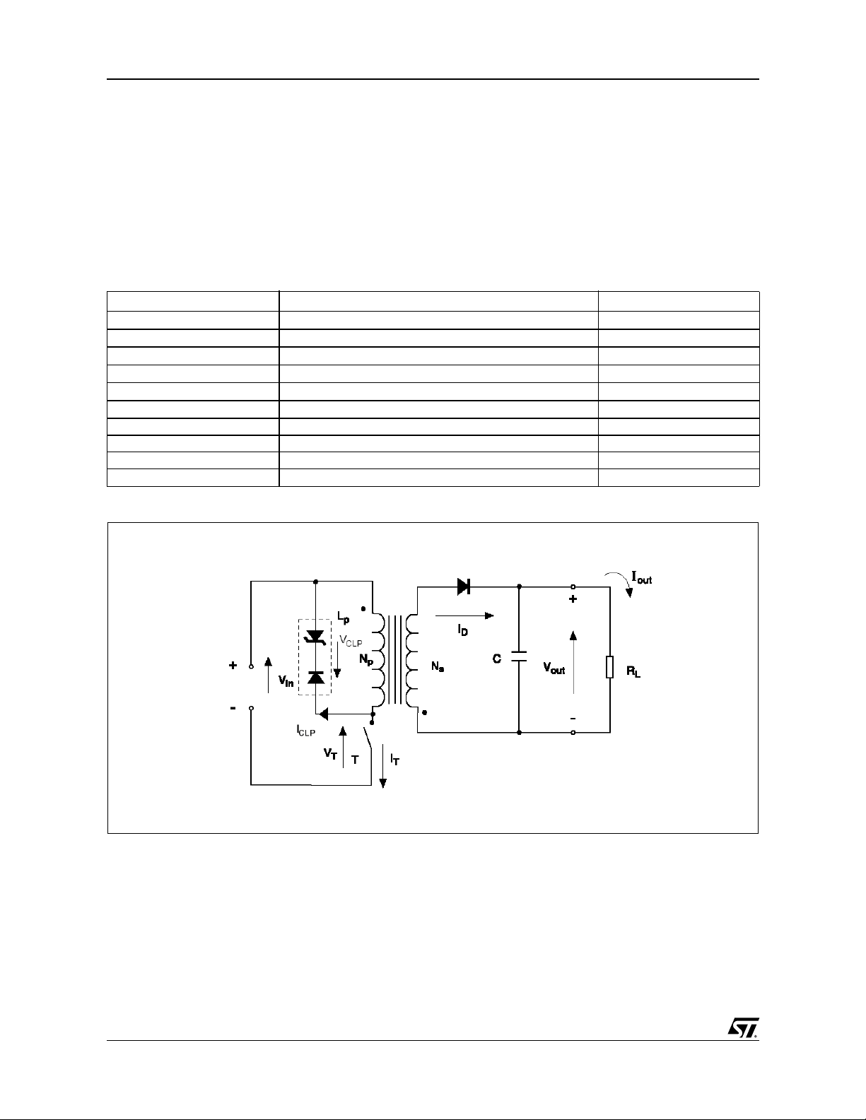
Figure 1 shows a simplified schematic diagram of
a flyback converter.
The discontinuous mode, shown in figure 2, has
no front-end step in its primary current, i
turn-off, the secondary current i
, is a decaying
D
, and at
T
triangle which drops to zero before the next turnon.
In the continuous mode, shown in figure 3, the
primary current i
characteristic appearance of a rising ramp on a
step. During the transistor off time (figure 3), the
secondary current has the shape of a decaying
triangle sitting on a step with the current still
remaining in the secondary at the instant of the
next turn-on. There is, therefore, still some energy
left in the secondary at the instant of next turn-on.
The two modes show significantly different
operating properties and usages. The
discontinuous mode responds more rapidly and
with a lower transient output voltage spike to
sudden changes in load current and input voltage.
On the other hand, discontinuous m ode provides
a secondary peak current in the range of two or
three times the continuous mode. This can be
easily understood by comparing figure 2 and figure
3.
The secondary current average v alue is equal to
the DC load current, as reported in both the above
mentioned figures. Assuming also closely equal
off time, it is obvious that the triangle in the
discontinuous mode must show a much larger
peak than the trapezoid of the continuous mode to
get the same average value. Therefore, in the
discontinuous mode, the larger secondary peak
current, at the beginning o f turn-off, will cause a
greater RFI problem.
Secondary rms current in the discontinuous mode
can be up to t wice that in the continu ous mode.
This requires larger secondary wire size and
output filter capacitors with larger ripple current
ratings for the discontinuous mode. Rectifier
diodes will a lso ha ve a high er tempe rat ure r ise in
the discontinuous mode because of the larger
secondary rms current.
Primary peak currents for the discontinuous mode
are about twice those in the continuous mode. As
a result, the discontinuous mode requires a higher
current rating and possibly a more expensive
power transistor. Also, the higher primary current
in the discontinuous mode results in a greater RFI
problem.
Despite all these relative disadvantages, the
discontinuous mode is much more used for low
has a front-end step and the
T
Rev. 1
1/27March 2005
Page 2
AN2131 - APPLICATION N OTE
power applications. This is due to two reasons.
Firstly, as mentioned above, the discontinuous
mode, with an inherently lower transformer
magnetizing inductance, responds more quickly
and with a lower transient output voltage spike to
rapid changes in output load current or input
voltage. Secondly, because the transfer function
of the continuous mode has a right half plane zero,
the error amplifier bandwidth must be drastically
consequence, the transient response is much
slower.
Finally, referring to the power spec of our demo, it
is clear that the discontinuous mode cannot be
used because it would determine a very high
primary and secondary peak current with a higher
cost of all the main components involved: power
transistor, secondary diode and output capacitor.
reduced to stabilize the feedback loop. As a
Table 1. Converter Specification data and Fixed Parameters
Symbol Description Values
V
inmin
V
inmax
V
out1
V
out2
V
aux
P
out
η Converter Efficiency >75%
F Switching frequency 90 kHz
Fsb Stand-by switching frequency 35 kHz
V
spike
Rectified minimum Input voltage 250
Rectified maximum Input voltage 850
Output voltage 1 24V/6.25A
Output voltage 2 5V/0.075A
Auxiliary Output voltage 15V/0.01A
Maximum Output Power 150W
Max over voltage limited by clamping circuit 200V
Figure 1. Simplified Schematic Diagram of a Flyback Converter
2/27
Page 3
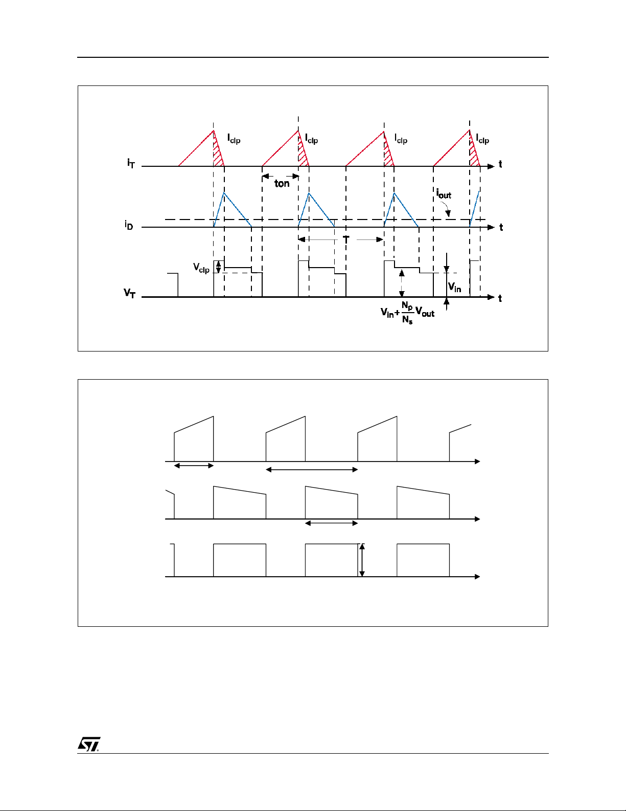
Figure 2. Discontinuous Mode Flyback Waveforms
t t
I
AN2131 - APPLICAT ION NOTE
Figure 3. Continuous Mode Flyback Waveforms
IT
t
D
VT
on
T
Ts
T
off
Vin+Vfly
3. FLYBACK CONTINUOS MODE WITH L5991
The minimization of the power drawn from the
mains under light load conditions (Stand-by,
Suspend or some o ther idle modes) i s an issue
that has recently become of great interest, mainly
because new and more severe standards are
coming into force.
The key point of this strategy is a low sw itching
frequency. It is well-known that many of the power
loss sources in a lightly loaded flyback waste
energy proportionally to the switching frequenc y,
hence this should be reduced as much as
possible. On the other hand, it is equally well-
3/27
Page 4

AN2131 - APPLICATION N OTE
D
V
D
N
V
known that a low switching frequency leads to
bigger and heavier magnetics and mak es filtering
more troublesome. It is then advisable to make the
system operate at high frequency und er nominal
load condition and to reduce the frequ ency when
the system works in a low-consumption mode.
This requires a special functionality of the
controller. It should be able to automatically
recognize the condition of light or heavy load and
then adequate its operating frequency
accordingly.
The L5991 PWM controller, with its "Stand-by
function", meets exactly this requirement. This
application note will deal with the design of a
flyback using L5991 PWM driver, while deeper
details about the driver itself can be foun d in the
dedicated application note AN1049.
The specifications table reports the two values of
the switching frequency, 90kHz for normal mode
and 35kHz for stand-by mode.
4. FLYBACK STAGE DESIGN
The continuous mode operation, as any switching
topology, is identified by observing the steady
state behavior of the energy storage compon ent.
In the flyback topology, the storage element is
represented by the magnetization transformer
inductance, which is charged by the primary
winding during the on time, and discharged by the
secondary winding during the off time. The flyback
topology will hence be working in continuous
mode if the secondary wind ing current does not
reach zero at the end of the off time.
As previously said, the mixed mode implies a
discontinuous mode operation for low load and/or
higher input voltage. The boundary depends on
the output power for a given input voltage. The
higher is the input voltage th e hig her is t he ou tput
power when the continuous mode starts.
Theoretically, there isn't any restriction to fix the
boundary between continuous and discontinuous
mode. It will be given by imposing design equation
for others relevant circuit parameters.
The maximum duty cycle , that in a discontinuous
mode flyback is imposed to prevent the continuous
mode operation, in this case must be fixed
establishing a good trade-off between primary and
secondary side performance. There are two
opposite effects: by inc reasing the duty cy cle the
rms current at primary side can be reduced , while
the rms current at secondary side will be
increased. This means that a higher duty cycle
imposes a less stressful cond ition to any part s in
the primary path, and a more stressful condition to
the secondary path. In the same way, to decrease
the duty cycle causes an optimization of
secondary side and a deterioration of primary side
performances.
The higher duty cycle is a further help to easily
design the flyback stage for a wi de range voltage
input. On the other hand, the higher duty cycle
implies a higher reflected voltage to promptly
demagnetize the flyback transformer.
For such a high power flyback stage, an important
parameter to monitor is the current ripple at
secondary side; it is needed either t o lower rms
current or to reduce RFI. Further consideration
concerns the reflected flyback voltage which is
imposed in order not t o overcome the maximum
breakdown of the power switch.
The above consideration plus some cost issues
generate a clear figure of how to impose design
equations. Moreover, since design specifications
imply a high power output only, the following
calculation will consider the influe nce of both low
power and auxiliary outputs negligible.
In continuous operation mode the relationship
between input and output voltage is only
dependent on the duty cycle and not on the
frequency. The relationship is given by the
following formula:
N
Out
V
in
D
S
11
−⋅=1
N
P
Eq. 1
Eq. 1 is ideal and does not take into consideration
real effects such as the voltage drops on the
power switch and on the output diode. I ncluding
these two voltage drops it is possible to get the first
design equation and calculate the turn ratio
between input and the higher power output
(Vout1).
N
P
=
N
S
1
Where, V
CSon
−
+
and V
VcsVin
on
VdVout
D
⋅
111
−
fw
are respectively the
d1fw
Eq. 2
voltage drop on the power switch and on the
secondary side diode. Eq. 2 is valid for any input
voltage. The second des ig n eq uat ion co mes from
the maximum power switch breakdown, defining
first V
, the flyback reflected voltage, and then
fly
calculating the maximum switch breakdown
voltage.
P
fly
()
N
S
VdVout
111+⋅=
fw
Eq. 3
4/27
Page 5

AN2131 - APPLICAT ION NOTE
in
V
0
s
V
V
3
8.
mVVVBV
arg
+++=
inspikefly
max
Eq. 4
Eq. 4 also includes the safe design margin and the
allowed voltage spike f ixed by clamping network
design. By combination of Eq. 3 and Eq. 4, the
maximum primary/secondary turn ratio is finally
obtained.
inmVVBV
arg
⇒
inmVVBV
Eq. 5
−−−≤
inspikefly
max
N
P
≤
N
S
1
inspike
+
arg
−−−
max
VV
fwdOu t
11
For 150W power output, the proposed power
switch is STC08DE150, with BV=1500V.
Assuming V
=1V. From Eq. 5 results:
V
d1fw
N
P
1
N
1≤S
From Eq. 2, imposing V
=200V, margin=200V and
spike
in=Vinmin
=220V, Np/Ns =
Eq. 6
10, and considering the normal mode switching
frequency, the maximum duty cycle and the maximum on time are:
N
P
=
N
Vfly
15=
+
VdVaux
fwaux
Eq. 10
The next transformer design step is to fix the
primary and/or secondary magnetization
inductances. There are several criteria: the first
one is to select the primary in duc tance in o rder to
ensure continuous mode operation from full load
to minimum load. This method, since a bigger
primary magnetization inductance is requested,
assures a very low output current ripple,
increasing transformer primary turns.
Furthermore, it makes the RHP zero lower, so that
the loop stabilization will be more complicated.
The second alternative criterion is to calculate
primary and secondary inductances by defining
maximum secondary ripple current. This last
method fixes a limit fo r the rms current and do es
not require such a high primary magnetization
inductance, but it may lead to a transition m ode
operation.
max
TonD
=
⇒
µ
87.5max%8.52
=
Eq. 7
It is worth noticing that the v al ue of t he duty cycle
calculated by Eq. 7 is a good trad e-off to optimi ze
both primary and secondary side performances.
By the way, it must be pointed out that being
>50%, slope compensation may be
D
max
necessary. This subject will be deeply analyzed in
paragraph 7.
Once fixed t he turn ratio between input a nd the
higher power output, the flyback reflected voltage
is fixed by Eq. 3 as well.
N
P
fly
()
N
1
S
VdVout
25011
=+⋅=
fw
Eq. 8
It is now possible to calculate the two turn ratios
referred to the slave Vout2 and to the auxiliary
outputs.
N
P
=
N
2
Vfly
2
3
=
+
VdVout
fwS
Eq. 9
5/27
Page 6
AN2131 - APPLICATION N OTE
t t
I
1
()
A
5
A
A
Figure 4. Waveforms and Nomencla ture of the Continuous Mo de Flyb ack Desi gn
Ipcs
∆
Ips
Ip
on
T
∆
Is1
s1
VT
Figure 4 reports the most significant waveforms
and relevant nomenclature to further proceed in
the flyback design. From figure 4, we define IPCS
the primary average current value and ∆
primary current variation during the on time, I
the secondary average current value and ∆
secondary current variation during the off time and
the secondary average current.
I
Out1
By adopting the second design method, we now fix
the maximum secondary ripple current ∆
following equations:
I
max1
Out
⋅∆⋅=⋅∆⋅=∆
IIII
SCSSSS
122D
−
max
where ∆
Ι
s1max
variation and ∆
1max1
is the maximum secondary current
Ι
is the ripple current. Therefore
s
we have:
TTVdV
−⋅−
L
()
=
1
S
where L
S1
inductance. Imposing ∆
I
∆
max!
S
is the secondary magnetization
max1
ONSfwOut
Ι
%= ±30% from Eq. 11
s
and Eq. 12 results:
IPS
IS1
Ι
% in the
s
Eq. 1
Eq. 12
the
S1CS
the
Ts
T
off
Once fixed turn ratios an d t he primary inductance
value, some extra calculation is needed to choose
either the transformer or the external components
for flyback stage. Since design specifications request one high power output only, while the slave
and the auxiliary outputs need a very small power,
for designing the transformer we can only consider
a single output. Based on this supposition the relevant design parameters are here below reported.
Fixed N
Primary Winding:
Ip
Ipcs
Is1cs
Iout1
Vin+Vfly
= 10 and Lp = 1.6 mH.
p/Ns
−
=∆ Eq. 1
on
max*)min(
TonVcsVin
8.0
=
Lp
Po
=
min
IpIp
+= Eq. 17
cspk
max
DVcsVin
η
max)(
⋅⋅−
on
Ip
∆
88.12=
48.1
=
t
Eq. 16
HL
µ
S
while the primary magnetization inductance is:
L
P
6/27
17.161= Eq. 13
2
N
P
=
N
S
S
1
Ip
=
rms
max
HL
µ
1617
=⋅
1
Eq. 14
=
A
08.1
∆
IpIpD
−=
cspk
I
1
P
2
IpIp
−−+
cspk
2
I
∆
P
=
23
Eq. 18
Page 7
AN2131 - APPLICAT ION NOTE
A
A
0
A
Is
1
5
1
Master Secondary Winding:
I
Out
Is
1
=
CS
=∆ Eq. 2
Is
1
1
=
Is
rms
()
29.9
=
max1
D
max1
−
IsIs
11 =
+=
CSpk
max
A
24.13
=
−⋅+
TTVdVout
)()1(
ONFW
max
Ls
1
∆
9.18
=
2
∆
I
1
IsIsD
111
s
−−=
cspk
3
2
IsIs
Eq. 19
7.9
Eq. 21
2
∆
I
11
s
−−+
11
cspk
2
Eq. 22
Above calculation have been made c onsidering a
continuous mode operation. This condition is
assured by imposing ∆I
%< 100%. According to
s
the reported design parame ters, the transformer
has been designed by Cramer and all remaining
power parts have been chosen as reported in ST's
application note AN1889.
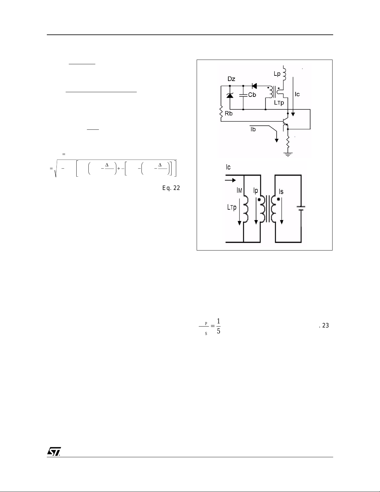
Figure 5. The Pro portional Driv in g Schematic
and its Equivalent Cir cuit
=
5. BASE DRIVING CIRCUIT DESIGN
In practical applications, such as SMPS, where the
load is variable, the collector current is variable as
well.
As a consequence, it is very important to provide
a base current to the device which i s r elated to the
collector one. In this way, it is possible to avoid the
device over saturation at low load and to optimize
the performance in terms of power dissipation.
The best and simplest way to do this is the
proportional driving method provided by the
current transformer, in figure 5.
At the same time, as already stated, it is very
useful to provide a short pulse to the base to make
the turn-on as fast as pos sible and to reduc e the
dynamic saturation phenomenon.
The pulse is achieved by using the capacitor and
the zener in figure 5.
The driving network guarantees a zone with f ixed
ratio that results imposed once the current
I
C/IB
transformer turn ratio h as been chosen. F rom the
ESBT STC08DE150 dat asheet, and in particular
looking at the st orage time characterization, it is
clear that a turn ratio equal to 5 is a good value to
ensure the right saturation of ESBT at I
= 2A, so
c
that in the current transformer we can fix at first:
N
P
=
N
S
Eq. 23
The core magnetic permeability of the current
transformer has to be as high as possible in order
to minimize the magnetization current I
(that is
m
not transferred to the secondary side but only
drives the core into saturation). On the contrary,
too high a permeability core may lead the core into
saturation even with a very small magnetization
current. To avoid that i t is necessary to increase
the number of primary turns and the size of the
core as well. On the other hand, if a core with a
very small magnetic permeability is chos en, it is
possible to reduce the number of primary turns
and the core size, but if the permeability is too
small we may not have current on t he secondary
side because almost all the collector current
7/27
Page 8

AN2131 - APPLICATION N OTE
TV
V
V
V
V
I
5
b
()
V
()
becomes magnetization current. As a compromise
a ferrite material with a relative permeability in the
range of 4500 ÷ 7000 is the best choice.
When a ferrite ring with some diameter has been
selected, the minimum primary turns is determined
to avoid the core saturation from the preliminarily
fixed turn ratio N with 0.2. By applying the
Faraday’s law and imposing the maximum flux
equals to B
B
max
N
1
d
ϕ
dt
sat
/2:
AN
B
∆
⋅⋅≅=
t
∆
⇒
N
TPeTPTP
⋅
on
2
=
max1
BA
sate
⋅
Eq. 24
Where, B
is the saturation flux of the core and it
sat
depends on the magnetic permeability.
During the conduction time, the junction base-
emitter of ESBT can be seen as a f orward b iased
diode. To complete the secondary side l oad loop
the voltage drop on both diode D and resistor R
must be added in series with the base of the
ESBT. The equivalent secondary side voltage
source is given by:
VVV
RBDBEonS
5.2≅++=
Eq. 25
Since the magnetization inductance cannot be
neglected, only I
, a fraction of the total collector
P
current, will be transferred to the secondary. As a
result, the magnetization current has to be first as
low as possible. Meanwhile, the value of the
magnetization inductance must be taken into
account for a proper calculation of transformer
primary turns and turns ratio. The magnetization
voltage drop, that is, the voltage at the primary of
the current transformer, can be now easily
calculated:
adjusted to get the desired I
ratio according to
C/IB
the equation below:
N
eff
where I
I
P
==
I
B
is the maximum magnetization
Mmax
II
−
maxmaxCMC
I
current.
The insulation between primary and secondary
should be considered since the voltage on the
primary side during the off time can overstep
1500V.
Next step is to select the zener diode, the
capacitor C
and the resistor Rb. The turn-on
b
performance of ESBT is related to the initial base
peak current and its duration t
approximately given by:
CRt3=
bpeak
B
A suitable value for R
is 0.56. It can eliminate the
b
ringing on the base current af ter the peak, and at
the same time, it generates negligible power
dissipation.
The value t
can be determined once the
peak
minimum on time is set based on the operation
frequency. Bear in mind that in practical
applications it should never be lower than 200ns.
The value of Cb can be counted since the values
of t
I
and Rb are known.
peak
must be limited in order to avoid an extra
peak
saturation of the device. This action is made by the
zener diode Dz that clamps the voltage across the
small capacitor Cb. The zener must be chosen
according to the following empirical fo rmulas and
bpeakZ
Zmin
12
+=
and V
Zmax
inside the range of V
max
RI
peak
:
Eq. 28
that is
Eq. 29
N
T
1
V
S
1
N
T
2
1
5.2
5
[]
V
5.0
=⋅==
The magnetization current will be:
Eq. 26
min
=
RIV2
bpeakZ
The base peak current will be higher with higher
Eq. 30
clamp voltage (Dz) o r smaller capacitanc e (Cb),
TV
ON
=
M
max
max1
L
TP
Eq. 27
which in tu rn will le ad to a shor ter dur ation of th e
peak time.
The higher and longer the base p eak current, the
lower the power dissipation during turn-on. But
The number of primary turns should be increased
if I
is relativ ely hig h. But the core mu st hav e
Mmax
window area enough to hold all primary and
secondary windings. Othe rwise it is necessary to
choose a bigger core size. Once both core
material and size are fixed, the turn ratio must be
you need to limit the Ib peak both in terms of
amplitude and time duration otherwise at low load
a very high saturation level may result. If the
device is over-saturated the storage time is too
long with higher power dissipation during turn-off.
Moreover a long storage time can also cause
output oscillation especially at high inpu t voltage.
8/27
Page 9

AN2131 - APPLICAT ION NOTE
G
1
)
)
G
2
To overcome the above mentioned problems it is
recommended to fix the peak duration to 1/3 the
minimum duty cycle.
6. CONTINUOS CURRENT MODE LOOP
STABILIZATION
It is well known from literature that the transfer
function of the continuous current mode (CCM)
flyback converter is given by:
sv
)(
1
out
s
)(
1
()
sCR
C
⋅
where N = N
electrolytic capacitor series resistance.
It is worth noticing that the transfer function has
one pole and two zeros, whose on e on the right
half plane. The RHP zero is very difficult if not
==
sv
)(
11
−+
2
sCR
1
+
D
+
, R is the load, RC is the
p/Ns
−⋅⋅
DRN
1(
⋅
+⋅⋅
DR
1(3
Scomp
DsL
p
2
()
1
−
DRN
Eq. 31
impossible to compensate and therefore must be
kept well beyond the closed-loop bandwi dth. As a
result, the transient response o f such system wi ll
be not extremely fast.
Considering now, the transfer function in the
following form:
)(
sv
out
comp
1
)(
sv
)(
s
1
⋅==
k
1
s
−
11
z
s
1
−
p
Substituting the values of this design in case of low
input voltage (worst case), we obtain the
frequency response reported in the following
figure 6. Poles and zeros are reported in the below
equations:
P11= -202/rad=-32.1Hz
= -23Krad/s=-3.79KHz
Z
11
Z
= 88Krad/s=14.1KHz
12
s
−
z
1211
Eq. 3
11
Eq. 33
9/27
Page 10

AN2131 - APPLICATION N OTE
G
G
s
G
1
Figure 6. Flyback Frequency Response at Minimu m Input Voltage
A good line and load regulation implies a high DC
gain, thus the open loop gain should have a pole
at the origin. Normally, in this case we need a
feedback network like the one in figure 7. Its
transfer function is given by:
sv
s
)(
2
out
==
sv
)(
)(
comp
or:
sv
)(
comp
s
)(
out
sv
)(
RCTR
COMP
max
FHB
−
1
1
k
==
22
s
1
−
()
1
1
sCRR
1
s
z
21
++
+
CsR
compCOMP
Eq. 34
Eq. 35
s
p
21
CRRs
To properly design the feedback loop, let us
consider first the following transfer function and its
bode plots (figure 8):
s
)(1⋅
FFH
It is preferable that the RHP zero is well bey ond
the closed loop cut off freq uency . To make it, first
of all, a gain is ne eded. Then, f rom figure 8, a 90
degrees phase margin could be achieved fixing
both zero and pole of G
pole p
get a phase margin of 90 degrees with a well
defined gain. Observe t hat a high phase margin ,
making the system response quite slow, could
help avoid undesired frequency changes. By the
way, to assure a not too slow trans ient response,
it is advisable to choose ab out 60 degrees phase
margin. Referring to this real case, we can fix both
zero and pole in order not to exactly cancel p
and z21.
and zero z21 of G1. In this case, we i deally
11
to cancel respectively
2
Eq. 36
11
10/27
Page 11

AN2131 - APPLICAT ION NOTE
Z
According to the previous argument we fix the pole
and zero as Eq. 37.
= -11.1krad/s = -1.77kHz
P
21
= -245rad/s = -39Hz
21
Eq. 37
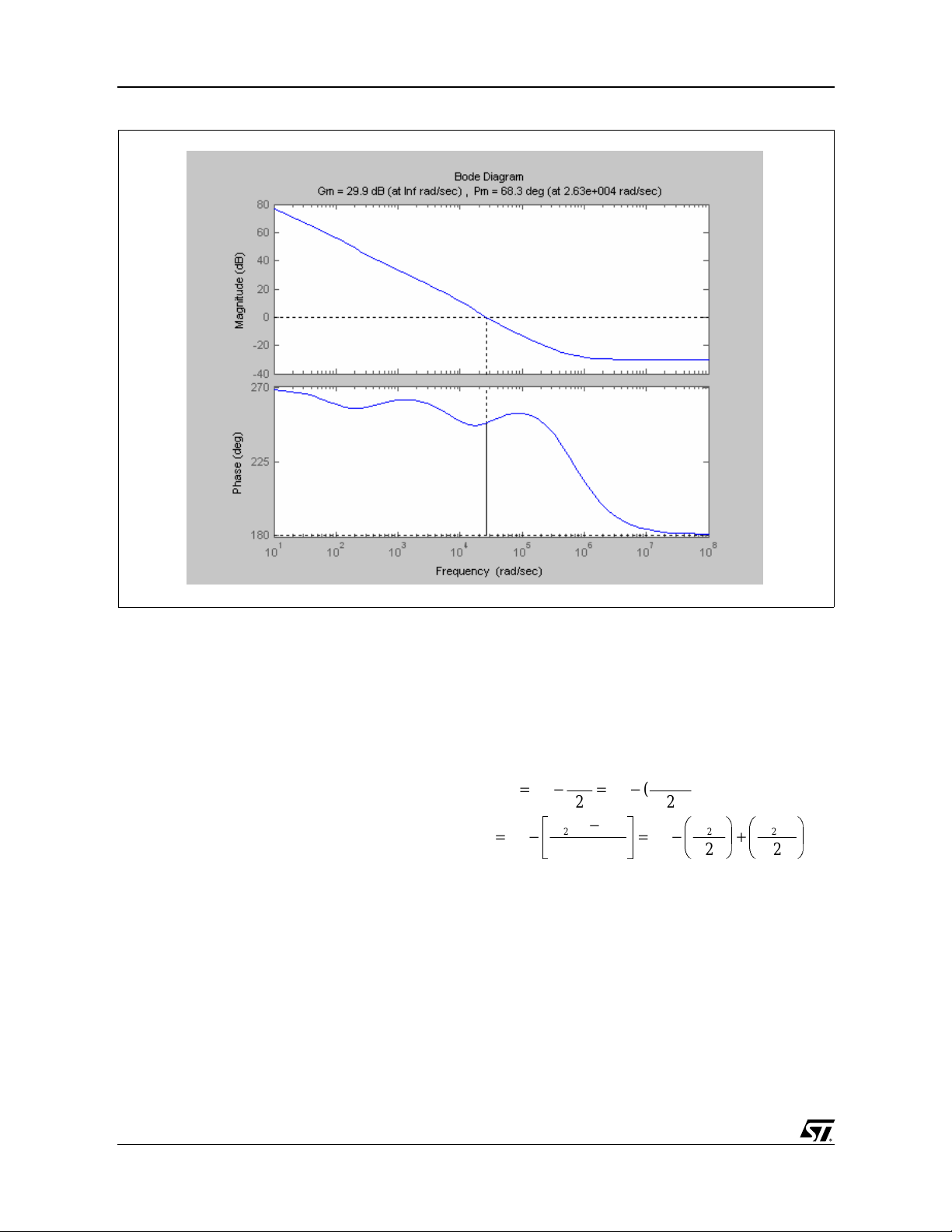
Figure 10 reports the overall open loop transfer
function G1*G2.
Phase margin is very close to the desired value
and it assures a good stability and quite fast
Figure 7. Converter Feedback Network
transient response. Finally, it is interesting to
check the loop stability for the highest input
voltage and maximum output load. Under this
condition, the frequency response of the system is
shown in figure 11.
From figure 12, as expected, the phase m argin is
higher and hence the system stability margin is
improved.
11/27
Page 12

AN2131 - APPLICATION N OTE
Figure 8. Flyback Frequency Response at Vinmin Adding a Pole at the Origin
Figure 9. Fre quency Response of the Feed bac k-transfer Function
12/27
Page 13

AN2131 - APPLICAT ION NOTE
Figure 10. St abi li ze d Op e n Lo op-transfer Function at Mini m um Input Voltage
Figure 11. Flyback Frequency Response at Maximum Input Voltage
13/27
Page 14
AN2131 - APPLICATION N OTE
Figure 12. Stabilized Open Loop-transfer Function at Maximum Input Voltage
voltage and which may continue for some time.
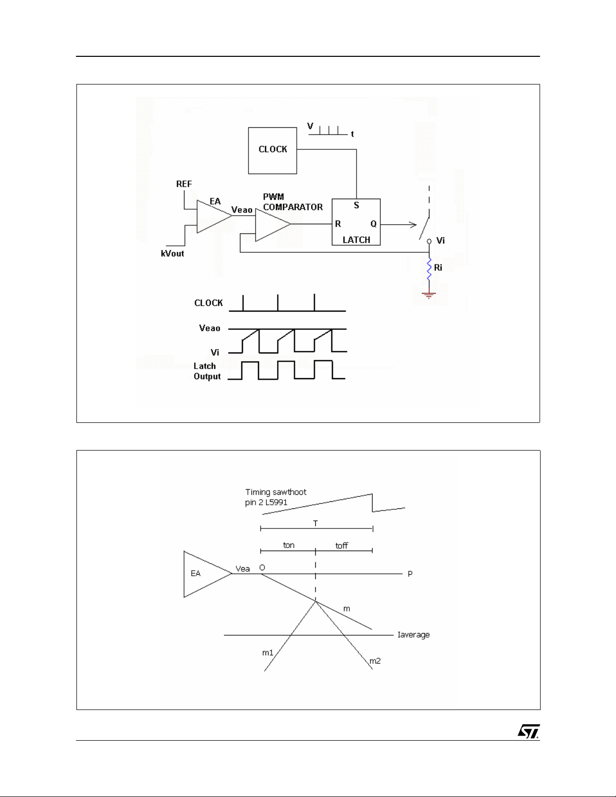
7. SLOPE COMPESATION FOR
SUBHARMONICS SUPPRESSION
The L5991, as many PWM drivers for SMPS,
applies a current mode control. This control
method keeps the power transistor current peak
constant at the needed level to supply the DC load
with DC output voltage dictated by the voltage
error amplifier. This is equal to keep cons tant the
current peak at secondary side winding. The
average current at secondary side is the DC load
current and, however, to keep the current peak
constant does not mean to keep the average
current constant.
Because of this, in the unmodified current mode
scheme, changes in the DC input voltage will
cause momentary changes in the DC output
voltage. The output voltage change will be
corrected by the voltage error amplifier outer
feedback loop, as this is t he l oop which ultimately
sets the output voltage.
Again, however, the inner loop, while keeping
peak inductor current constant, does not supply
the correct average current and output voltage
changes again. The effect is then an oscillation
which commences at every change in input
The mechanism can be better understood from an
examination of the upslope and do wnslope of the
output inductor currents.
In figure 13, it can be seen that the average
primary side current at low DC input is higher than
the high DC input case. This can be seen
quantitatively as:
dI
2
II
−=
I
p
I
ppav
2
()
−
tTm
on
tm
2
off
=−=−=
(
)
2
Tm
I
−=
p
tm
on
222
222
Eq. 38
+
14/27
Page 15

AN2131 - APPLICAT ION NOTE
Figure 13. Average Primary Side Current at
Low and High DC Input
Since the voltage feedback loop keeps the product
of V
constant, at lower DC input voltage,
dcton
where the on time is higher, the average output
inductor current I
is higher, as can be seen from
av
equation 38 and figure 13.
Furthermore, since the DC output voltage is
proportional to the average, not to the peak,
inductor current, as DC input goes down, DC
output voltage will go up.
DC output voltage will then be corrected by the
outer feedback loop and a seesaw action or
oscillation will occur.
A second problem whi ch generates oscillation in
current mode is shown in figures 14 and 15.
From these figures, it can be seen that, at a fixed
DC input voltage, if for some reason there is an
∆I
initial current disturbance
, after a first
1
downslope the current will be displaced by an
∆I
amount of
.
2
Figure 14. Current Disturbance Effects at Duty
Cycle <50%
Figure 15. Current Disturbance Effects at Duty
Cycle >50%
Furthermore, if the duty cycle is less than 50%
(m
) as in figure 14, the output disturbance ∆I
2<m1
will be less than the input disturbance ∆I1, and
after some cycles, the disturbance will die out. But
if the duty cycle is greater than 50% (m
2>m1
) as in
figure 15, the output disturbance after one cycle is
greater than the input disturbance.
This can be seen quantitatively from figure 14. For
∆I
a small current displacement
, the current
1
reaches the original peak val ue earlier in time by
∆I
an amount dt where dt =
. On the inductor
1/m1
downslope, at the end of the on time, the current is
lower than its original value by an amount
∆I
where
m
2
Now with m
IdtmI ∆==∆
122
m
1
grea ter tha n m1, the disturbances will
2
Eq. 39
continue to grow but eventually will decay, causing
an oscillation.
Both current-mode problems mentioned above
can be corrected as shown in figure 16, where the
original, unmodified output of the error amplifier is
shown as the horizontal voltage level OP. The
scheme for correcting the previous problems
(slope compensation) consists of adding a
negative voltage slope of magnitude m to the
output of the error amplifier. By a proper selection
of m in the way discussed below, the inductor
average DC current can b e made independent of
the power transistor on time. This corrects the
problems indicated in both equations 38 and 39.
Figure 17 shows the upslope m1 and the
downslope of the output inductor current.
Remember that in current mode, the power
transistor on time starts at every clock pulse and
ends at the instant the output of the PWM
comparator reaches equality with the output of the
voltage error amplifier as shown in figure 16.
2
2
15/27
Page 16
AN2131 - APPLICATION N OTE
Figure 16. PWM with Current Mode Control
Figure 17. Implementation of Slope Compensation
16/27
Page 17

AN2131 - APPLICAT ION NOTE
n
i
R
V
)
V
0
0
n
V
In slope compensation, a negative voltage slope of
magnitude m=dV
added to the error amplifier output. The magnitude
of m is, therefore, calculated.
In figure 17, the error-amplifier output at any time
after a clock pulse is
t
on
eaea
0
where V
to zero.
The peak voltage V
sensing resistor R
is the error amplifier output at ton equal
ea0
==
where Ipp and Isp are the primary and secondary
currents respectively. But I
is the average secondary or average output
inductor current and dI
inductor current change during the off time (m
Then
II −+=+=
sasp
Then
N
s
i
N
Equating eq. 40 and 41, which is wh at the PWM
comparator does, we obtain
N
s
N
p
N
s
−
N
p
IR
p
m
2
R
i
2
/dt starting at clock time is
ea
mtVV−=
o
across the primary current-
i
in figure 16 is
i
N
s
IRI
spippi
N
p
+ dI2/2, where I
sp=Isa
, in figure 13, is the
2
tm
2
off
m
2
(
I
tT
22
m
2
()
2
tVIR
0
oneasai
T
−+=
tT
onsai
N
N
m
2
s
R
p
−+=
i
2
Eq. 40
Eq. 41
sa
2toff
Eq. 42
onsa
Eq. 43
−
m
Eq. 44
This, then, corrects the two above mentioned
problems arising from the fact that without
compensation, current mode maintains the peak
constant, and not the average, output inductor
current.
The same effect is obtained by adding a positivegoing ramp to the output of the current-sensing
resistor V
voltage unmodified.
Adding the positive-going ramp to V
is the most usual approach. Let us suppose that
the slope of the ramp is dV/dt.
When the PWM driver finds the equality of its two
inputs, the output terminates the on time. Then
+(dV/dt)ton=V
V
i
N
s
N
p
Then
).
N
s
N
p
t
From the above, it can be seen that if the slope dV/
dt of the voltage added to V
N
p)Rim2
relation vanish and the secondary average voltage
is independent of the on time.
I
sa
In the L5991 chip, a positive going ramp starting at
every clock pulse is available at the top of the time
capacitor (pin 2 in figure 18).
The voltage at that pin is:
osc
and leaving the error-amplifier output
i
subs titute Vi from e q . 4 1 :
ea0
IR
dV
on
dt
/2, the terms involving ton in the preceding
∆
=
∆
m
2
()
−+
IR
tT
2
N
sai
N
N
−+
N
V
t
o
t
m
s
p
s
p
2
R
R
T
i
2
m
2
2
dV
dt
++
V
=
eai
is equal to (Ns/
i
is simple and
i
Vt
=+
eaononsai
Eq. 46
Eq. 47
Eq. 48
It can be seen in this relation that if
N
N
then the coefficient of the t
average output inductor current is independent of
the on time.
m
s
p
2
R
i
2
m
dV
ea
==
dt
term is zero and the
on
Eq. 45
where
∆V = 2V and ∆t = 0.693*R
tCt
.
17/27
Page 18

AN2131 - APPLICATION N OTE
n
V
Figure 18. Slope Compensation by Simple Resistance
As seen in figure 18, a fraction of that voltage
whose slope is ∆V/∆t is added to V
(the voltage
i
across the current-sensing resistor). That slope is
set at (N
s/Np)Ri(m2
/2) by the Rcs, R
Thus in figure 18, since R
is much less than Rcs,
i
slope
resistors.
the voltage delivered to the current sensing
terminal (pin 13) is:
R
+
i
CS
RR
+
slopeCS
VV
iosc
R
+=
CS
RR
+
V
∆
t
o
t
∆
slopeCS
Eq. 49
and setting the slope of that added voltage equal
=
slopeCS
+ R
/2), we obtain
mRNN
()()
).
tCt
drain current off the top of the
slope
2//
iPS
2
tV
∆∆
Eq. 50
to (N
s/Np)Ri(m2
R
CS
RR
+ /
where ∆V/∆t = 2/(0.693R
Since R
CS
timing capacitor, the operating frequency
changes.
Then either R
CS
+ R
is made large enough so
slope
that the frequency change is small or an emitter
follower is interposed between pin 2 and the
resistors as shown in figure 19.
Figure 19. Slo pe C om pensation by E m itte r
Follower Stage
We choose the second option for two reasons: the
first one is due to the fact that it is difficult to avoid
frequency changes with typical R
values. The
CS
second reason, related to the L5991 characteristics, is a little bit more complicated and it will be
now explained.
In our design, after choosing R
R
CS
+
RR
()()
=
slopeCS
iPS
∆∆
/
= 1kΩ we have:
CS
mRNN
2//
2
tV
k
9.6
Ω≅
Eq. 51
18/27
Page 19

AN2131 - APPLICAT ION NOTE
V
The closest value available is R
= 6.8kΩ.
slope
Therefore, first of all, to keep the frequencies
established originally, the oscillator res istors can
be chosen accordingly, and more important, since
the valley value of the oscillator is about 1V, we
have a voltage shift of:
R
CS
=∆
V
i
+
1 =
RR
slopeCS
1
=
VV
+
8.61
m
1281
Eq. 52
As already stated in the previous paragraphs, the
PWM driver used in our design has a special
feature. We can externally fix two different
operating frequencies in order to improve the
system power efficiency.
As mentioned in both AN1049 and
L5991datasheet, the level at which the operating
frequency changes is es tablished by Vcomp, the
error amplifier output voltage. Two thresholds are
used to guarantee a hysteresis, avoiding
Figure 20. Final Slope Compensation Schematic
uncertainty when switching from low to high
frequency and vice-vers a. As explained in the
AN1049 the two values can be referred to the
current sensing (pin 13) voltage. The upper level is
0.867V while the lower level is 0.367V.
If a simple resistance is used to ma ke the slope
compensation, a voltage shift is also introduced
and its value computed in eq.52 is too high. In fact,
to make the system work at low frequency it is
necessary to undergo 0.367V and it may happen
that the lower frequency is never reached.
With the emitter follower of figure 19, besides
avoiding any alteration in the oscillator
functionality, we get about 0.5V voltage shift
respect to pin2, and hence a consequent reduction
of the ∆V
previously calculated. To obtain ∆Vi = 0
i
and assure the correct behavior of the PWM driver
in the SMPS a diode in series with the emitter has
been introduced as shown in figure 20.
19/27
Page 20

AN2131 - APPLICATION N OTE
5A
8. PROTOTYPE IMPLEMENTATION AND EXPERIMENTAL RESULTS
Figure 21. Prot otype Schematic
24V @ 6.2
1
2
J2
H2
C13
1nF
22
R27
0.5W
T1
1000uF
50V
C15
+
1000uF
50V
C14
+
D9
STTH3002CT
16
15
9
10
CSM 39-07 1 B
1
7
3
D7
STTH108
D6
1.5KE400A
D5
STTH108
6.8nF/1250V
C9
47k
R20
2W
47k
R21
2W
24k
R31
18k
R29
4k7
R28
PC817
U2A
1
2
1
2
J3
5V @ 0.05A
C17
100nF
Vout
GND
Vin
U3
L78L05
C16
+
47uF 25V
D10
STTH102
14
12
4
5
47uF
25V
STTH102
D8
+
C11
D4
1N4148
2k7
R30
C18
150nF
TL4 31 A C
U4
C12
1nF/Y1
H1
0.56
R26
STC08DE150
46
T2
1
STTH 102
.22uF
D2
Q1
R25
T34 8 36
3
D3
R22
C10
0.56
3.9V
R11
56k
0.56
R23
R24
1k
22
20/27
470pF
R10
240k
0.5W
R9
240k
400V
240kR30.5W
0.5 W
820k
R6
1
2
Vin 250VDC to 850VDC
820k
R7
R8
R17
220uF
400V
C2
+
R1
F1
R18
-t
6k8
8k2
10/3.7A
T1A
5k6
R15
R14
NU
D1
1N4148
14
16
13
15
12
dis
isen
St-by
sync2rct3dc
U1
1
R16
Q2
6k8
R13
sgnd
dc-lim
vref5vfb
4
12k
PN2222A
910k
910kR5910k
R4
220uF
C1
+
240kR20.5W
J1
C8
9
11
10
vc
out
pgnd
22
R19
vcc
comp
L5991A
47uF
C6
C5
C4
C3
43
U2B
50V
C7
+
NU
3.3nF
100nF
10nF
PC817
6
7ss8
470
R12
Page 21

AN2131 - APPLICAT ION NOTE
The theoretical design has been further improved
by bench verification getting the final schematic
reported in figure 21. The board has been
successfully tested according to design
specifications previously reported and additional
features have been also verified.
At that time there is still current flowing through it
and therefore forces a hard turn-off which caus es
ringing on the reverse recovery.
By adding a snubber based on a capacitance
higher than the diode junction capacitance and a
resistor tuned to the ringing of the leakage
inductance and the diode c apacitance, the peak
D6 Snubber Circuit
This topology works both in discontinuous and
continuous mode.
The output diode turns off at zero current when
operating in discontinuous mode after the core is
discharged. In continuous mode the diode turns off
when Q1 is turned on.
reverse voltage spike and the ringing can be
minimized.
The ringing often causes EMI issues and adds
noise to sensitive PWM circuits. Figure 22 shows
the diode at 6 amps.
The blue waveform is the diode recovery without
snubbing, while the green one is the diode
recovery after adding the snubber.
The resistor dissipates 0.23 watts in this example.
Figure 22. D6 Diode Recovery Time Effects with and without Snubber
21/27
Page 22

AN2131 - APPLICATION N OTE
Short Circui t
During an output overload or short circuit, the
primary current ramps up higher and higher. This
current is sensed by R8 which is turned into a
voltage, filtered by R17 and C10 and fed to pin 13
of U1 (I sense). When this voltage reaches 1 volt
the pulse is terminated. This is known as pulse by
pulse current limit. The unit is protected against
overstressing the main switch and output diode. In
other words by choosing R8 we can limit the power
of the unit. During short circuit the output power is
limited to this value. Depending on the transformer
coupling an output short should reflect a lower
voltage to the auxiliary voltage supplying the
L5991. When this voltage falls below the under
voltage lockout of 8.4 volts, the L5991 shuts down
and initiates a restart. In most cases because of
the insulation in a transformer, it is difficult to
achieve such results. As shown in figure 23, when
the output is overloaded the transformer voltage
falls to about 3 to 4 volts due to the drop of the
diode traces and the output inductor. The 24 volts
winding has 10 turns and the Vcc one has 6, so the
voltage at the transformer pin of Vcc should be
around 2.2 volts. The problem is the leakage
inductance causing spikes and ringing whose
peak charge the Vcc cap. as seen in figure 23
(violet waveform).
Figure 23. Output Waveforms without Short Circuit Protection
22/27
Page 23

AN2131 - APPLICAT ION NOTE
By adding a 22uH inductor in series with the Vcc
winding and D3 we are a ble to filter out the s pike
and ringing to achieve Vcc to collapse below the
under-voltage shutdown and re-initiate a start up.
In this mode the high-cup mode is reached
dissipating less power and keeping the thermal
stresses low.
The shutdown is shown in the Figure 25 at 300V
input. The hiccup mode duty cycle is 45ms on and
370ms off. As the input voltage is increased, the
start up through resistors R25 becomes faster
decreasing the off time. At 850 volt in the duty
cycle is decreased to 50% protecting the power
devices.
The most meaningful wavefo rms at different load
and input conditions are reported in figures 26, 27,
28, 29.
Figure 24. Output Waveforms with Short Circuit Protection
Figure 25. Hic cup Mode with Short Ci rc ui t Pro t ec tio n
23/27
Page 24

AN2131 - APPLICATION N OTE
Figure 26. Steady State Vin=850V Pout=150W
Figure 27. Steady State Vin=850V Pout=150W
Figure 28. Steady State Vin=250V Pout=150W
Figure 29. Steady State Vin=250V Pout=150W
Figure 26, 27, 28, and 29 show the prototype
steady state behavior, by reporting the gate
voltage (violet waveform), the ba se current (blue
waveform), and the collector current (yellow
waveform) signals. The collector voltage signal
has been not caught under maximum load
condition because the probe parasitic capacitance
generates an inner loop noise causing some
undesirable oscillations.
TM
Of course, safe operation for the ESBT
in terms
of maximum voltage spike on the collector has
been also verified.
The switching frequency under maximum load
condition is about 85Khz. The base current
waveform highlights as the ESBT
TM
storage time
is about 600ns, indicating the correct device
saturation level and hence its optimal working
condition.
Next waveforms will show the low l oad condition
where the switching frequency is appreciably
reduced to optimize, even in this condition, the
power supply efficiency.
24/27
Page 25

AN2131 - APPLICAT ION NOTE
Figure 30. Steady State Vin=850V Pout=25W
Figure 31. Steady State Vin=850V Pout=25W
Figure 33. Steady State Vin=250V Pout=25W
Figure 30, 31, 32 and 33 show the steady state
behavior for the low load condition. I n this case the
switching frequency is about 37KHz, and the
collector voltage signal (green waveform) has
been added sin ce in this less stressful con dition
the probe doesn't affect the system stability. From
figure 31 is possible to see the very high voltage
applied on the collector (1184V) during a normal
working condition.
Figure 32. Steady State Vin=250V Pout=25W
25/27
Page 26

AN2131 - APPLICATION N OTE
9. PCB LAYOUT
Figure 34. Prot otype PCB Lay o ut
The printed circuit board is reported in figure 34,
while the relevant bill of material is listed in the
schematic of figure 21.
REFERENCES:
- STMicroelectronics application note AN1889
"ESBT STC03DE170 IN 3-PHASES AUXILIARY POWER SUPPLY"
- STMicroelectronics application note AN1049
"MINIMIZE POWER LOSSES OF LIGHTLY
LOADED FLYBACK CONVERTERS WITH
THE L5991 PWM CONTROLLER "
- STMicroelectronics L5991 datasheet
- STMicroelectronics STC08DE150 datasheet
- Abraham I. Pressman, "Switching Power Supply
Design", McGraw-Hill, Inc.
26/27
Page 27

AN2131 - APPLICAT ION NOTE
Information furnished is believed to be accurate and reliable. However, STMicroelectronics assumes no responsibility for the consequences
of use of such information nor for any infringement of patents or other rights of third parties which may result from its use. No license is granted
by implic ation or oth erwise under any patent or patent righ ts of STMicroele ct ronics. Spe ci f i cations menti oned in this publication are subjec t
to change without notice. This publication supersedes and replaces all information previously supplied. STMicroelectronics products are not
authori zed for use as criti cal components in life supp ort devices or s ys tems without express writt en approval of S T M i croelectronics.
The ST logo is a register ed t rademark of STMicroelec tr onics.
All other nam es are the property of their respective owners
© 2005 STMi croelectroni cs - All rights reserved
STMicroelectronics group of companies
Australi a - Belgium - Brazil - Canad a - China - Czech Republic - Finl and - France - Germany - Hong Kong - India - Israel - Italy - Ja pan -
Malaysia - M al ta - Morocco - Singapore - Sp ai n - S weden - Swit zerland - Uni te d Kingdom - Un i ted States of A m eri ca
www.st.com
27/27
 Loading...