

Page 1
AN2129
APPLICATION NOTE
DIMMING OF SUPER HIGH BRIGHTNESS LEDS
WITH L6902D
1 Introduction
Thanks to the high efficiency and reliability, super high brightness LEDs are becoming more
and more important when compared to conventional light sources. Although LEDs can be supplied directly from a simple voltage source (like battery with resistor), for most applications it
is better to use a switching current source to get not even higher efficiency but also to get a
better light output. This paper will focus on a L6902D based DC/DC converter with dimming
interface. For more details about other converters and applications for LEDs available from
STMicroelectronics please refer to other application notes ([1] and [2]).
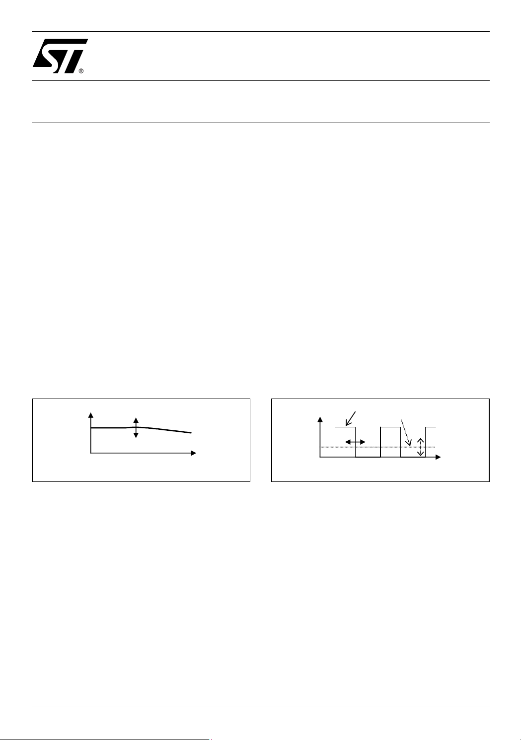
2 Dimming Concepts
There are two basic principles how the light output of the LED can be controlled. Since the light
brightness is proportional to the current, both methods are dealing with current regulation. The
first and the easiest way is to control the LED current itself, with the principal sketch in Figure
1, where current is changed proportionally with the dimming signal. Disadvantage of this analog control is that there can be a significant change of color (wavelength difference could be
several nanometers) in deep dimming (less that 10%). This potential disadvantage is compensated by a very simple control circuit (usually a simple potentiometer is enough).
Figure 1. Analog current control Figure 2. Average current control by PWM
I
time
The second method is based on an average current control (digital control) as can be seen in
Figure 2. The current is switched between zero and the nominal current with a frequency higher than 100Hz (to avoid flickering). The change of duty cycle and hence the average current
change will be seen as a brightness change, because human eye reaction is slow enough to
"integrate" the light output and it will not be noticed as a blinking.
This method avoids the color change problem, but on the other hand it needs more sophisticated control circuits (usually a microcontroller or another simple PWM generator).
I
I
I
time
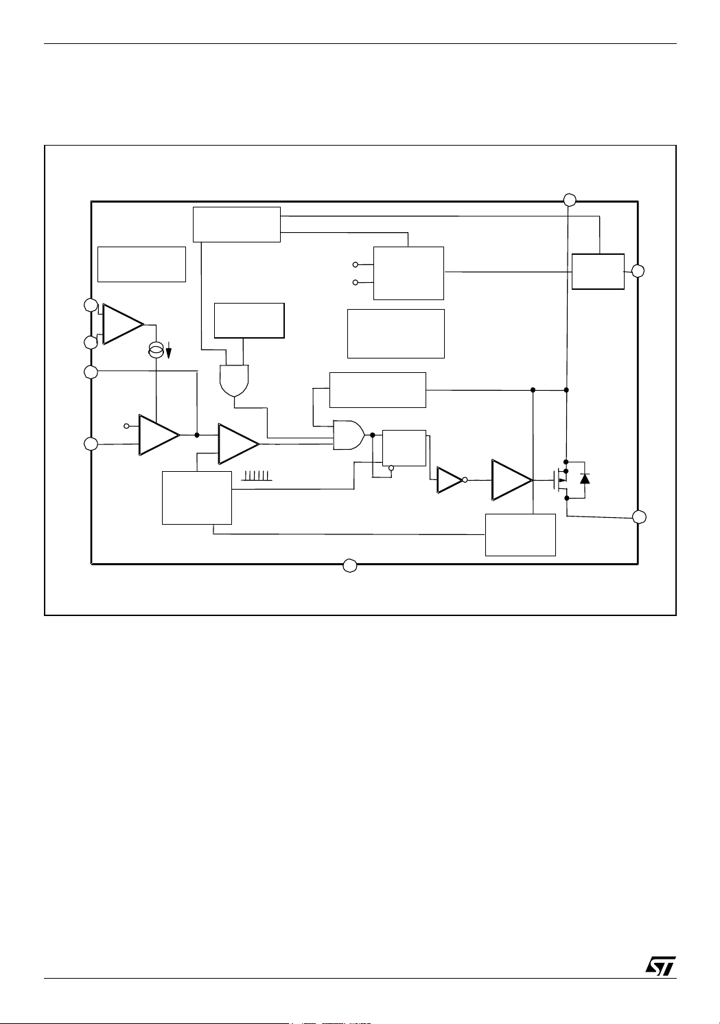
3 L6902D DC/DC Converter
The L6902D is a complete and simple step down switching regulator with adjustable current
and voltage feedback. Thanks to its current control loop with external sense resistor it is able
to work in a constant current mode, providing up to 1A output current with an accuracy of 5%.
Among other features there can be also found general purpose 3.3Volts precise (2%) reference voltage or 2.5A (typical value) internal current limit for short circuit protection.
AN2129/0705
Rev. 2
1/9
Page 2
AN2129 APPLICATION NOTE
In Figure 3 is the internal structure of the L6902D converter, the datasheet [3] should be referred for more details.
Figure 3. L6902D Block diagram (see [3] for details)
V
cc
VOLTAGES
MONITOR
V
ref
CS+
CS-
INHIBIT
Current_E/A
+
-
THERMAL
SHUTDOWN
3.8V
1.235V
SUPPLY
TRIMMING
VREF
GOOD
COMP
VFB
1.235V
Voltage_E/A
+
E/A
-
OSCILLATOR
-
PWM
+
PEAK TO PEAK
CURRENT LIMITING
D
CK
GND
Q
DRIVER
OUT
FREQUENCY
SHIFTER
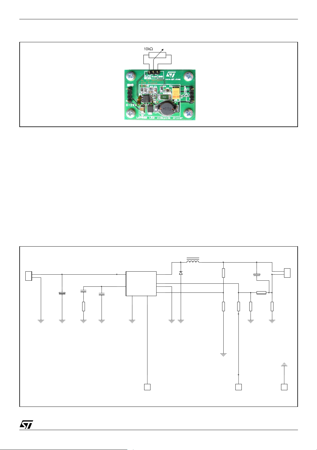
4 Application Board
An application board using the dimming principles described above has been designed and its
schematic is in Figure 5. There is only a single dimming input connector on the board; usable
for both dimming methods (either analog or PWM control can be used, as preferred). There
were made some changes compared to the application circuit presented in datasheet [3] allowing this dimming. First of all, the sense resistor has been moved from higher voltage path
(coil output) to the lower one (output ground). Then three resistors were added (R4, R5 and
R6) for modifying the current sense feedback.
A signal between 0 and 3.3V should be used for analog (peak current) dimming. When the
dimming pin is grounded (0V) the maximum output current is provided (350mA) and vice versa
when 3.3V is applied to the pin, the current provided is zero and so the LED is off. There are
two more pins on the board: 3.3V reference voltage pin and ground pin (a jumper can be used
to connect the dimming pin to the ground pin for the maximum output). For the easiest way of
dimming just connect the 10kΩ potentiometer between 3.3V and ground pins. The potentiometer slider should be connected to the dimming pin (as it can be seen in Figure 4).
2/9
Page 3
AN2129 APPLICATION NOTE
Figure 4. Connecting the potentiometer for analog dimming
The second dimming method implemented on this board is a PWM control of average LED current. This control needs a digital PWM signal (amplitude can be either 3.3V or 5V) between
dimming pin and ground pin. Then varying the duty cycle will change the LED brightness
(100% means LED off and 0% means LED fully on).
With the closer look on the application (Figure 5) it is noticeable that cathode of the LED must
not be connected to the ground of the circuit, because there is a sense resistor between cathode and the ground. If by any accident, LED cathode is grounded, the current feedback loop
will be inactivated and the L6902D will set the maximum output voltage (as set by the voltage
divider R1 and R3) regardless the current which can eventually destroy the LED. Also care
must be taken on input voltage polarity together with output LED polarity. If the input polarity
is twisted, the whole IC could be damaged. While with the output polarity reversed, the board
itself cannot be damaged, but the LED will see the maximum voltage (as limited by the voltage
divider R1 and R3) in reverse direction.
Figure 5. Board schematic (order code STLEDDCDIM-EVAL1)
L1
100uH
J1
8 - 24V
2
1
C1
+
10uF
25V
CERAMIC
R2
5k1
C3
22nF
C4
220pF
L6902D
U1
8
VCC
4
COMP
GND
7
OUT
CS+
CS-
VREF
6
1
J3
3.3V Vref
1
2
3
5
FB
D1
STPS34OU
Rsense
0.33
J2
1
2
Output
1
J6
GND
R1
9k1
R3
510
R6
27k
1
J4
Dimming Input
C2
+
10uF
35V
1k
R4
R5
8k2
3/9
Page 4

AN2129 APPLICATION NOTE
Figure 6. PCB layout
Table 1. Bill of materials
Type Reference Part Supplier Order Code
Ceramic Capacitor C1 10uF N/A
Tantal Capacitor C2 10µF; 35V N/A
Capacitor SMD 0805 C3 22nF N/A
Capacitor SMD 0805 C4 220pF N/A
Schotky Diode D1 STPS340U STMicroelectronics
Connector J1 8 -24V N/A
Connector J2 Output N/A
Connector J3 3.3V Vref N/A
Connector J4 Dimming Input N/A
Connector J6 GND N/A
Coil L1 100µH; 1.2A; 0.33Ω Würth Elektronik 744 562 0
Resistor SMD 2010 Rsense 0.33 N/A
Resistor SMD 0805 R1 9k1 N/A
Resistor SMD 0805 R2 5k1 N/A
Resistor SMD 0805 R3 510 N/A
Resistor SMD 0805 R4 1k N/A
Resistor SMD 0805 R5 8k2 N/A
Resistor SMD 0805 R6 27k N/A
Converter U1 L6902D STMicroelectronics
The calculation of the resistor current feedback network can look relatively complicated, but
with few simplifications it becomes easy to take in. First assumption is that all the current flows
only through the R
of R
is defined by the output current and the threshold voltage on CS+ pin (100mV). Un-
sense
(i.e. neglecting voltage drop on the resistors R4,R5 and R6); the value
sense
fortunately this calculation will give uncommon values (e.g. for 350mA it gives 0.2857Ω) thus
the nearest higher standard (e.g. E24 series) value for Rsense should be selected (e.g. 0.33Ω)
and then the difference between ideal and standard value is compensated by R4, R5 and R6
to receive precise output current.
The application is shifting between two limit states with dimming; maximum current (zero dimming voltage) and zero current (full dimming voltage). In Figure 7, the dimming network with
grounded dimming input (Equation 1 describes the circuit) is shown, it means when the current
flowing through the LED is on its maximum (i.e. 350mA on this board).
4/9
Page 5

AN2129 APPLICATION NOTE
Figure 7. Dimming network with zero dimming voltage (maximum current)
V
= 0V
dimm
⋅⋅ ⋅
100mV
R5 R6 I
-------------------------------------------------------------------------- -=
R4 R5⋅ R4 R6⋅ R5 R6⋅++
LEDRsense
Eq 1
The second limit state is depicted in Figure 8. In this case the current through the Rsense is
zero (LED is off) and thus on point A there is a zero voltage (i.e. ground). The Equation 2
shows the calculation for this state.
Figure 8. Dimming network with maximum dimming voltage (zero output current)
V
= 3.3V
dimm
100mV V
=
dimMAX
-------------------------------------------------------------------------- -
R4 R5⋅ R4 R6⋅ R5 R6⋅++
R4 R5⋅
Eq 2
5/9
Page 6

AN2129 APPLICATION NOTE
Both equations (Equation 1 and Equation 2) must be valid together, i.e. two equations for three
variables (I
LED
, R
sense
and V
dimMAX
should be selected before). One resistor must be chosen
before and than the other resistors calculated from the equations mentioned. This process
should be iterative (calculated for different chosen resistors) to get resistor values as close to
the industrial standard values as possible. The Table 2 can help for work simplification, because it contains resistor values for the most common super high brightness LEDs.
Table 2. Pre-calculated standard values for feedback loop
I
[mA]* V
LED
350 3.3 330 1000 8200 27000
700 3.3 200 910 2400 20000
1000 3.3 120 910 5600 24000
* ILED is a nominal LED current obtained with minimum dimming voltage (Vdimm=0V)
** VdimMAX means dimming voltage for maximum dimming i.e. zero output current (ILED=0A)
[V]** R
dimMAX
sense
[mΩ]
R4 [Ω]R5 [Ω]R6 [Ω]
5 Measurement
A couple of measurements have been performed on the board; the results are on the graphs
below. One up to six LEDs in serial string have been used as load (Golden Dragon LW W5SG
from OSRAM)
In Figure 9 there is a LED current waveform during dimming with PWM signal at 100Hz frequency. It could be noticed a waveform rounding during turning-on and off, which is caused by
charging the output capacitor C2. If the sharper on and off edges are needed a smaller capacitor should be used (e.g. 1µF), but on the other side it must be taken in account that it will rise
the current ripple.
Figure 9. PWM dimmin g (50%) Figure 10. Current rip ple
(1 LED, 15V input, 0% dimming)
6/9
Page 7

AN2129 APPLICATION NOTE
]
In Figure 10 the detail of output current is depicted, where the ripple during all the measurement stayed below ±5mA, (i.e. less than 2%). And as mentioned above, if a less wavy output
is needed, bigger output capacitor should be used, but then a slower on and off edges will appear.
Efficiency of the converter is processed in Figure 11 and Figure 12, where it is showed that
more difference between input and output voltage or lower load current, causes lower efficiency. For six LEDs in one serial string (voltage drop around 20Volts) and input voltage 25V the
efficiency was measured above 93%.
Figure 11. Efficiency vs. input voltage (@ 350mA output current)
100.0
95.0
90.0
85.0
80.0
Efficiency [%
75.0
70.0
0 5 10 15 20 25 30
1 LED 2 LEDs 3 LEDs 4 LEDs 5 LEDs 6 LEDs
Figure 12. Efficiency vs. number of LEDs @ 25V
100
95
90
85
80
75
Efficiency [ %]
70
65
60
01234567
LEDs
Input V olta ge [ V]
Figure 13. Output current variation
360
350
340
330
320
Output Current [mA]
310
300
01234567
LEDs
Increasing the number of LEDs in series in one string (on Figure 13) a lower output current can
be observed (for six LEDs it is 341mA instead of 350mA). That means less than 3% difference,
what should be still acceptable especially considering 5% precision of the current sensing amplifier in L6902D.
7/9
Page 8

AN2129 APPLICATION NOTE
The average value of the output current during dimming is depicted in Figure 14 and Figure
15. Almost ideal dimming curve can be observed during digital control (Figure 15). On the analog dimming curve (Figure 14) it can be seen that current is already zero for 3.1V in place of
3.3V. This behavior is caused by the use of industrial resistances (E24 values) instead of the
exact values calculated from Equation 1 and Equation 2 and it allows to have LED safely off
when maximum dimming voltage is applied.
Figure 14. Output Current during analog dimming
Figure 15. Output current during digital dimming
6 References and Related Materials
[1] AN1891 - Application ideas: Driving LEDs using L497x, L597x, L692x DC-DC converters
families
[2] AN1941 - Low voltage LED driver using L6920D, L4971 and L6902D
[3] L6902D Datasheet
7 Revision History
Table 3. Revision History
Date Revision Description of Changes
02-Mar-2005 1 First Issue
05-Jul-2005 2 Corrected the Eq. 2 to page 5/9
8/9
Page 9

AN2129 APPLICATION NOTE
The present note which is for guidance only, aims at providing customers with information regarding their products in
order for them to save time. As a result, STMicroelectronics shall not be held liable for any direct, indirect or
consequential damages with respect to any claims arising from the content of such a note and/or the use made by
customers of the information contained herein in connection with their products.
Information furnished is believed to be accurate and reliable. However, STMicroelectronics assumes no responsibility for the consequences
of use of such information nor for any infringement of patents or other rights of third parties which may result from its use. No license is granted
by implication or otherwise under any patent or patent rights of STMicroelectronics. Specifications mentioned in this publication are subject
to change without notice. This publication supersedes and replaces all information previously supplied. STMicroelectronics products are not
authorized for use as critical components in life support devices or systems without express written approval of STMicroelectronics.
The ST logo is a registered trademark of STMicroelectronics.
All other names are the property of their respective owners
© 2005 STMicroelectronics - All rights reserved
Australia - Belgium - Brazil - Canada - China - Czech Republic - Finland - France - Germany - Hong Kong - India - Israel - Italy - Japan -
Malaysia - Malta - Morocco - Singapore - Spain - Sweden - Switzerland - United Kingdom - United States of America
STMicroelectronics group of companies
www.st.com
9/9
 Loading...