

Page 1

AN2123
Application Note
TD351 Advanced IGBT Driver
Principles of operation and application
by Jean-François GARNIER & Anthony BOIMOND
1 Introduction
The TD351 is an advanced IGBT driver with integrated control and protection functions. It is a simplified
version of the TD350, available in an SO8 or DIP8 package. The TD35x family (including the TD350,
TD351 and TD352) provides a wide range of drivers specially adapted to drive 1200 V IGBTs with current
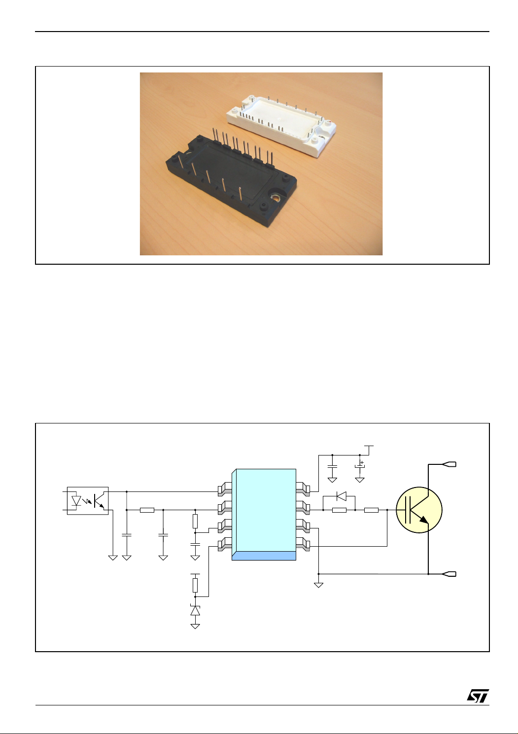
ratings of 15 to 75 A in Econopak-like modules (see Figure 2).
The main features of the TD351 are:
- 1 A sink/0.75 A source peak output current minimum over the full temperature range (-20°C to
125°C),
- active Miller clamp function to reduce the risk of induced turn-on in high dV/dt conditions, and in
most cases, without requiring a negative gate drive,
- optional 2-step turn-off sequence to reduce over-voltage in case of an over-current or a short-
circuit situation; a feature that protects the IGBT and avoids RBSOA problems,
- input stage compatible with both an optocoupler and a pulse transformer.
Applications include three-phase full-bridge inverters such as in motor speed control and UPS systems
(see Figure 1).
Figure 1. TD351 in 3-phase inverter application (1200 V IGBTs)
V+ DCbus
High-side power
supply
or
Bootstrap
Circuitry
Low-side power
supply
TD351
TD351 TD351 TD351
TD351
Phase 1
TD351
Phase 2 Phase 3
V- DCbus
AN2123/0205 Revision 1 1/15
Page 2
TD351 application example AN2123
VH
10K
11V
100nF
4K7
10nF
100pF
16K
470pF
16V
22Ω 22Ω
1
2
3
4 5
6
7
8
TD351
CD
IN
VREF
LVOFF
OUT
VL
CLAMP
VH
Figure 2. IGBT modules
2 TD351 application example
A TD351 application example is shown in Figure 3. In this example the device is supplied by a +16V
isolated voltage source. An optocoupler is used for input signal galvanic isolation. The IGBT is driven by
44Ω for turn-on and 22Ω for turn-off thanks to the use of two gate resistors and one diode: sink and
source currents can therefore be tuned independently to help and solve EMI issues. Power switch drivers
are used in very noisy environment and decoupling of the supplies should be cared. In the application
example the decoupling is made by a 100nF ceramic capacitor located as close as possible to the TD351
in parallel with a bigger electrolytic capacitor.
Figure 3. TD351 application example
2/15
Page 3
AN2123 Input stage
K
K
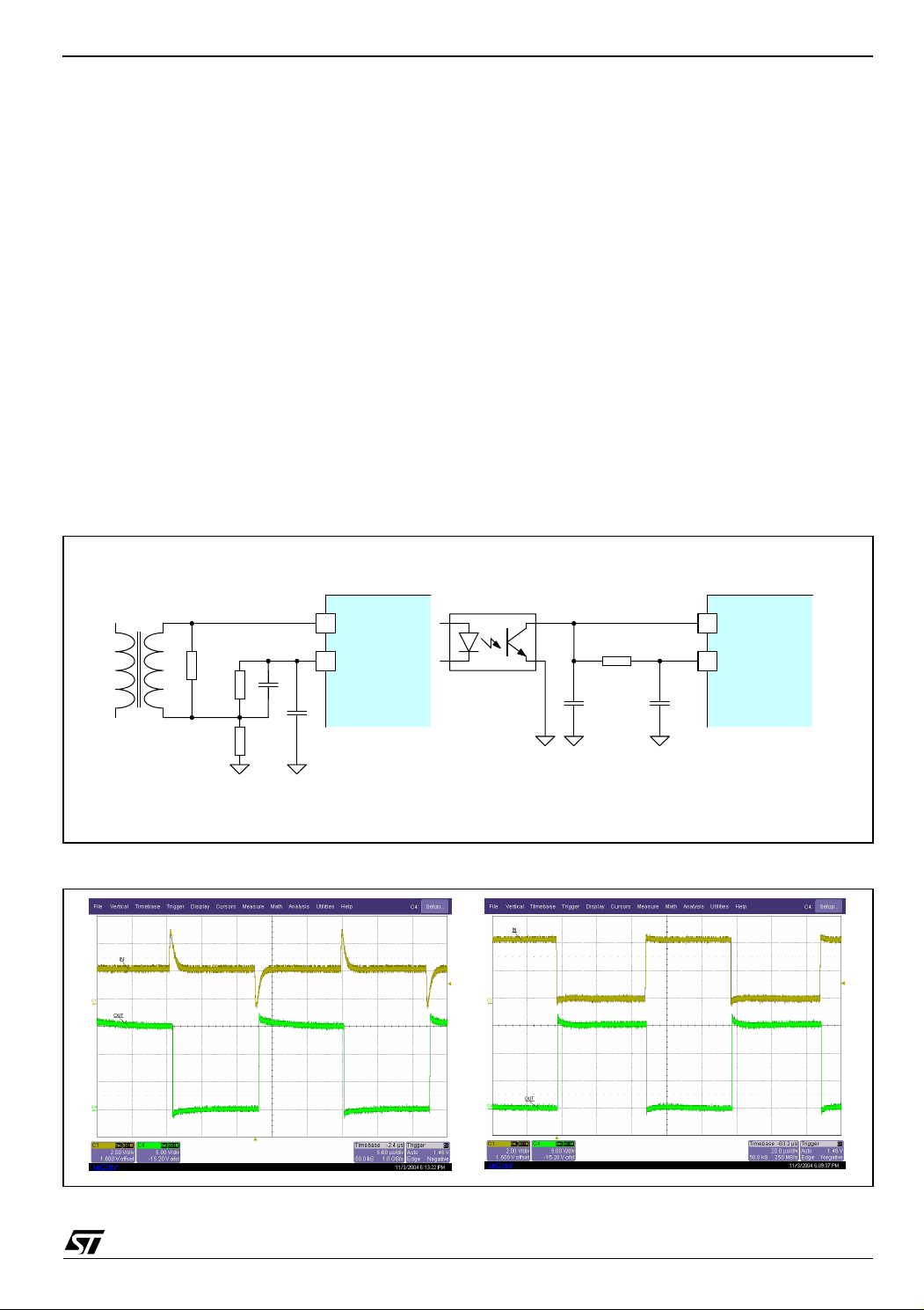
3 Input stage
The TD351 is compatible with the use of both pulse transformers or optocouplers. The schematics shown
in Figure 4 can be considered as example of use with both solutions.
When using a pulse transformer, a 2.5 V reference point can be built from the 5 V VREF pin with a
resistor bridge. The capacitor between the Vref and the bridge middle point provides decoupling of the
2.5 V reference, and also insures a high level on IN input at power-up, in order to start the TD351 in the
OFF state.
When using an optocoupler, the IN pin can be pulled-up to Vref. The pull up resistor is to be chosen
between 5 kΩ to 20 kΩ depending on the characteristics of the optocoupler. An optional filtering capacitor
can be added in case of a highly noisy environment, although the TD351 already includes filtering on
input signals and rejects signals smaller than 135 ns (t
Waveforms from the pulse transformer must comply with the t
Figure 5). To turn TD351 output on, the input signal must be lower than 0.8 V for 220 ns minimum.
Conversely, the input signal must be higher that 4.2 V for 220 ns minimum in order to turn off TD351
output. A pulse width of about 500 ns at the threshold levels is recommended. In all cases, input signal at
the IN pin must be between 0 and 5 V.
Figure 4. Application schematic (pulse transformer at left; optocoupler at right)
specification).
onmin
onmin
and V
ton/Vtoff
specifications (see
Pulse transformer Optocoupler
TD351
IN
1IN
VREF
2
10K
10
10
10nF
TD351
1
VREF
2
4K7
10nF
100pF
Figure 5. Typical input signal waveforms with pulse transformer (left) or optocoupler (right)
3/15
Page 4
Output stage AN2123
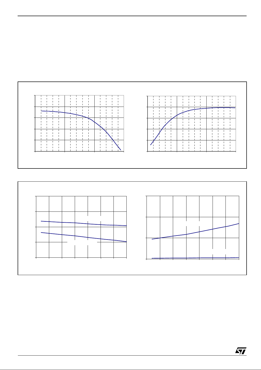
4 Output stage
The output stage is able to sink/source about 1.7 A / 1.3 A typical at 25°C with a voltage drop VOL/VOH
of 6 V (see Figure 6). The minimum sink/source currents over the full temperature range (-20°C/+125°C)
are 1 A sink and 0.75 A source. VOL and VOH voltage drops at 0.5 A are guaranteed to 2.5 V and 4 V
maximum respectively, over the temperature range (see Figure 7). This current capability sets the limit of
IGBT driving, and the IGBT gate resistor should not be lower than about 15Ω.
Figure 6. Typical Output stage current capability at 25°C (VH=16V)
OUT source current versus voltage (turn-on)
2.5
2.0
1.5
Iout (A)
1.0
0.5
0.0
0 5 10 15
Vout (V)
2.5
2.0
1.5
Iout (A)
1.0
0.5
0.0
OUT sink current versus voltage (turn-off)
051015
Figure 7. Typical VOL and VOH voltage variation with temperature
High level output voltage vs. Temperature
4.0
3.0
Iosource=500mA
2.0
VH-V OH (V)
1.0
Iosourc e=20mA
3.0
2.0
VOL-VL (V)
1.0
Low level output voltage vs. Tempera ture
Vout (V)
Ios ink= 500mA
4/15
0.0
-50 -25 0 25 50 75 100 125
Tem p (°C)
Iosink =20mA
0.0
-50 -25 0 25 50 75 100 125
Tem p (°C)
Page 5
AN2123 Active Miller clamp
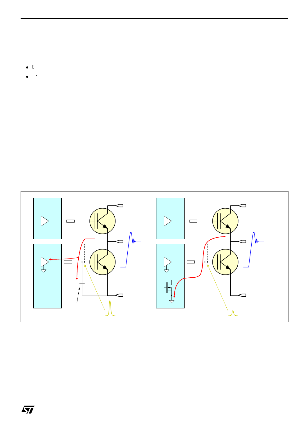
5 Active Miller clamp
The TD351 offers an alternative solution to the problem of Miller current in IGBT switching applications.
Traditional solutions to the Miller current problem are:
l
to drive the IGBT gate to a negative voltage in OFF-state in order to increase the safety margin
l
or, to implement an additional capacitor between the IGBT gate and collector as described in the lefthand schematic in Figure 8)
The solution proposed by the TD351 uses a dedicated CLAMP pin to control the Miller current. When the
IGBT is off, a low impedance path is established between IGBT gate and emitter to carry the Miller
current, and the voltage spike on the IGBT gate is greatly reduced (see the right-hand schematic in
Figure 8). The CLAMP switch is open when the input is activated and is closed when the actual gate
voltage goes close to the ground level. In this way, the CLAMP function doesn’t affect the turn-off
characteristics, but simply keeps the gate at a low level during the entire off-time.
The main benefit is that negative supply voltage can be avoided in most cases, allowing for the use of a
bootstrap technique for the high-side driver supply, and a consistent cost reduction for the application.
In addition, the use of the active Miller clamp feature avoids the need to implement any additional
capacitors between the IGBT gate and the collector. Such capacitors would negatively affect the ability of
the driver to control turn-on and turn-off.
Figure 8. Active Miller Clamp: principles of operation
High-side
driver
Low-side
driver
Miller current Miller current
high dV/dt !
10nF
optional capacitor
implemented to
reduce voltage spike
voltage spike on IGBT gate !
High-side
TD351
Low-side
TD351
active clamp
10R10R
no need for
additional
capacitor
high dV/dt !
reduced voltage spike
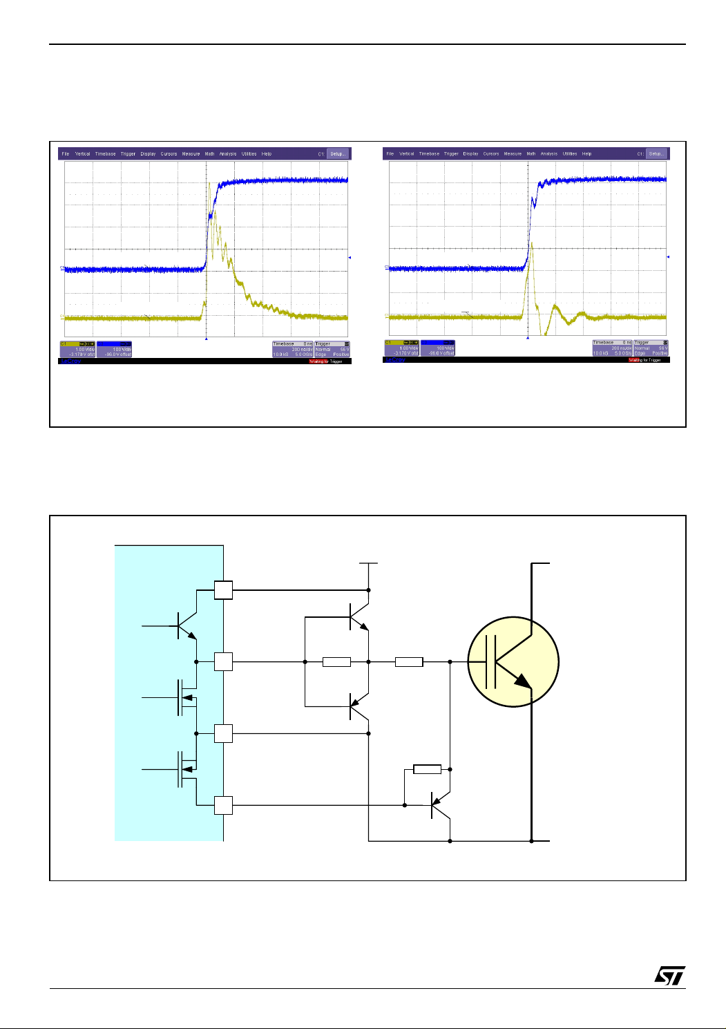
The test results shown in Figure 9 prove how the active Miller clamp results in a consistent reduction of
the voltage spike on IGBT gate.
The left-hand waveform shows the result of a 400 V switching with a 10 nF additional Gate to Emitter
capacitor to control the voltage spike on gate.
5/15
Page 6
Active Miller clamp AN2123
7
6
OUT
VL
8
VH
5
CLAMP
TD351
VH
T1
T2
T3
The right-hand waveform shows the results of the test in the same conditions but without any additional
capacitors and with the active Miller clamp.
Figure 9. Active Miller clamp: test waveforms related to above schematic
Vc e (100V /di v)
Vge (1V/div)
without Miller clamp
Vgs spike up to 6V!
Vce (100V/div)
Vge (1V/div)
Miller clamp implemented
in the same conditions,
the Vgs spike is reduced to about 3V
For high-power applications, buffers can be used to increase the output current capability. Figure 10
shows a schematic principle with external buffers for both the driver output and the clamp function.
Figure 10. Using external buffer to increase the current capability of the driver and clamp outputs
6/15
Page 7

AN2123 Active Miller clamp
For very high-power applications, the active clamp function cannot replace the negative gate drive, due to
the effect of the parasitic inductance of the active clamp path. In these cases, the application can benefit
from the CLAMP output as an secondary gate discharge path (see Figure 11 below).
Figure 11. High power application: negative gate drive and secondary gate discharge path
16V
-10V
VH
1
2
3
4 5
IN
VREF
CD
LVOFF
TD351
VH
OUT
CLAMP
8
7
6
VL
T1
T2
T3
With the above schematic, when the gate voltage goes close to VL+2 V (i.e. the IGBT is already driven
off), the CLAMP pin is activated. Again, the benefit is to lower the resistance between gate and emitter
when the IGBT is in the OFF state without affecting the IGBT turn-off characteristics.
Tip: What should one do with the CLAMP pin when not used in application?
Connect CLAMP to VL.
7/15
Page 8

2-Level turn-off AN2123
6 2-Level turn-off
In the event of a short-circuit or overcurrent in the load, a large voltage overshoot can occur across the
IGBT at turn-off and can exceed the IGBT breakdown voltage. By reducing the gate voltage before turnoff, the IGBT current is limited and the potential over-voltage is reduced. This technique is called 2-level
turn-off. Both the level and duration of the intermediate off level are adjustable. The duration is set by an
external resistor/capacitor in conjunction with the integrated voltage reference for accurate timing. The
level can be easily set by an external Zener diode, and its value is chosen depending upon the IGBT’s
characteristics. This 2-level turn-off sequence takes place at each cycle; it has no effect if the current
doesn’t exceed the normal maximum rated value, but protects the IGBT in case of overcurrent (with a
slight increase to conduction losses).
The principle is shown on Figure 12. During the 2-level turn-off time, the OUT pin is controlled by a
comparator between the actual OUT pin and an external reference voltage. When the voltage on OUT
goes down as a result of the turn-off and reaches the reference threshold, then the OUT output is
disabled and the IGBT gate is discharged no further. After the 2-level turn-off delay, the OUT output is
enabled again to end the turn-off sequence.
To keep the output signal width unchanged relative to the input signal, the turn-on is delayed by the same
value than the 2-level turn-off delay (see Figure 13).
Figure 12. Principle schematic for 2-level turn-off feature
VREF
VH
3
4
CD
LVOFF
2,5V
Lvoff off
120µA
Control
Block
OUT
VL
7
6
The duration of the 2-level turn-off is set by the external Rd-Cd components, and is approximately given
by the formula:
(in µs) = 0.7 * Rd (in kΩ) * Cd (in nF)
T
a
Recommended values are R
from 10kΩ to 20kΩ, and Cd from 100 pF to 470 pF, providing a range of
d
delay from about 0.7 to 6.6 microseconds.
8/15
Page 9

AN2123 2-Level turn-off
Figure 13. Waveforms of the 2-level turn-off function (COFF timing exaggerated for illustration)
Practical tests were made with 1200 V - 50 A IGBT modules Fuji 6MBI50S120L. The results shown in
Figure 14 point out how the 2-level turn-off feature can consistently reduce voltage stress on the IGBT in
the event of over-current.
During this test, the 50 A-rated IGBT module has to turn-off a 300 A current simulating an application
faulty condition.
The left-hand graph in Figure 14 shows a standard commutation. The driver OUT pin voltage is abruptly
pulled from 16 V to 0 V and the IGBT gate is discharged through the gate resistor. The fast turn-off of the
IGBT generates a voltage spike on Vce reaching 1kV, which is dangerously close to the IGBT absolute
maximum rating (1200 V). The calculated turn-off energy reaches 19 mJ.
The right-hand graph in Figure 14 shows how the TD351 and its 2-level turn-off feature can help deal with
this situation. During the first phase, the TD351 OUT pin is pulled from 16 V to 9 V during 2.5 µs. In the
second phase the OUT pin is pulled to 0 V. As a consequence, the IGBT turn-off is slightly longer and the
Vce voltage spike is advantageously reduced to 683 V. The calculated turn-off energy reaches 31 mJ,
but the resulting overheating can be more easily managed than the destruction of the IGBT by overvoltage stress.
Figure 14. Reduction of IGBT over-voltage stress using 2-level turn-off feature
Ic=300A
IGBT Vge
TD351 OUT
overshoot 1kV
Vce =400V
Ic=300A
IGBT Vge
TD351 OUT
overshoot 683V
Vce =400V
standard com muta tion
2-leve l turn-off w ith LVoff=9V
9/15
Page 10
2-Level turn-off AN2123
)
)
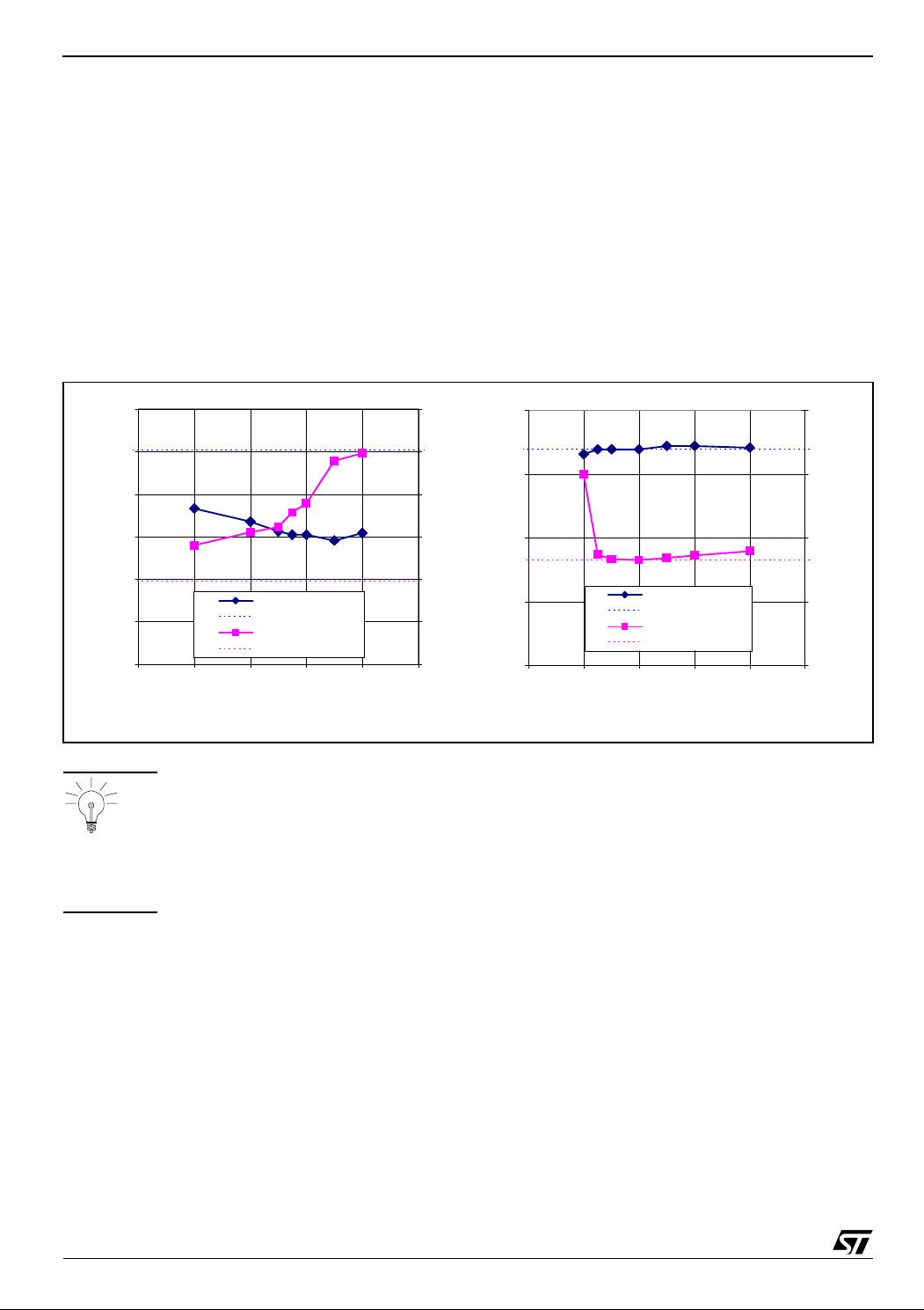
Maximum voltage reached on the IGBT collector and commutation losses are shown in the charts of
Figure 15. The influence of the LVoff value is studied both for nominal rated current at 25°C (75 A) and
over current (300 A) conditions.
It can be noted that in over-current conditions (see Figure 15, left graph) the 2-level turn-off can bring a
significant reduction of Vcemax during turn-off. With LVoff values from 8 to 11 V, Vcemax is reduced from
1000 V to less than 750 V. The price to pay is an increase of the switching losses Eoff that are shifted
from 20 mJ to 30~40 mJ.
In normal conditions (see Figure 15, right graph) there is no noticeable difference to be seen regardless
wheter the 2-level turn-off feature is used or not, as long as LVoff is greater than 8.5 V.
These results suggest that it is useful to set the LVoff value from 9 to 10 V.
Figure 15. Influence of LVoff value on Vcemax and turn-off energy (IGBT Fuji 6MBI50S120L)
1200
1000
800
600
Vce max (V)
400
Vce max 2-level
200
0
7 8 9 101112
over-current conditions: 400V/300A
Vce max standard
Eoff 2 -level
Eoff standard
Lvoff (V)
60
50
40
30
20
10
0
800
600
400
Eoff (mJ
Vce max (V)
200
0
7 8 9 10 11 12
Tip: How does one disable the 2-level turn-off feature?
Connect LVOFF to VH, remove C
capacitor and keep the CD pin connected to Vref by a
d
4.7 kΩ to 10 kΩ resistor.
Vce max 2-level
Vce max standard
Eoff 2 -level
Eoff s ta ndar d
Lvoff (V)
norma l condi tions: 400V/ 75A
8.00
6.00
4.00
Eoff (mJ
2.00
0.00
10/15
Page 11

AN2123 Application schematic
7 Application schematic
The TD351 application design presented hereafter is based on the active Miller clamp concept. With this
function, the high-side driver can be supplied with a bootstrap system instead of using a floating positive/
negative supply. This concept is applicable to low- and medium-power systems, up to about 10 kW. Main
benefit of this is to reduce the global application cost by making the supply system simpler. Figures 16
shows the half bridge design concept using the TD35x.
It should be highlighted that the active Miller clamp is fully managed by the TD35x and doesn’t require any
special action from the system controller.
Figure 16. TD35x application concept
24V
15V
5
Rb
+
Cb 4.7u
15V
Vreg
VREF
4k7
IN
VREF
4k7
IN
high side
TD35x
TD35x
VH
OUT
VL
CLAMP
VH
OUT
VL
CLAMP
The TD351 is able to drive 1200 V IGBT modules up to 50 A or 75 A (depending on IGBT technology and
manufacturer). Key parameters to consider are the TD351 peak output current (0.75 A source / 1.0 A
sink) and the IGBT gate resistor.
The values of gate resistors should be chosen starting with the recommended values from the IGBT
manufacturer. Thanks to the active Miller clamp function, the gate resistor can be tuned independently
from the Miller effect, which normally puts some constraints on the gate resistor. The benefit is to optimize
the turn-on and turn-off behavior, especially regarding switching losses and EMI issues.
Table 1 shows the recommended gate resistors values from two major IGBT module manufacturers, and
the peak gate current (with a 15 V supply) required for 10 A to 100 A IGBT modules. Approximate
application power is indicated.
11/15
Page 12

Application schematic AN2123
Table 1. Recommended gate resistors
Eupec:
FPxxR12KE3
Rgate
15 25 40 50 75 A
75 36 27 18 5 Ω
Ipeak 0.2 0.4 0.55 0.8 3A
Fuji:
6MBIxxS-120
Rgate
10 15 25 35 50 75 100 A
120 82 51 33 24 16 12 Ω
Ipeak 0.12 0.2 0.3 0.45 0.6 0.9 1.3 A
App. Power
1.5234571115 kW
IGBT modules suitable for TD351 are indicated in bold. For the FP50R12KE3 and 6MBI75S-120
modules, the source (charging) peak current will be limited to 0.75 A in worst-case conditions instead of
the theoretical 0.8 A or 0.9 A peak values; this usually doesn’t affect the application performance.
An external buffer will be required for higher power applications.
A reference schematic is shown in Figure 17. It uses a bootstrap principle for the high-side driver supply.
A very simple voltage regulator is used in front of the TD351 high-side driver. In this way, the bootstrap
supply voltage can be made significantly higher than the target driver supply, and the voltage across the
Cb bulk capacitor can exhibit large voltage variations during each cycle with no impact on the driver
operation.
Gate resistor Rg depends on the IGBT. It should be noted that the applications only use two supplies
referenced to the ground level.
12/15
Page 13
AN2123 Application schematic
Figure 17. TD351 Application Schematic with 2-Level Turn-off
TD351
high side drivers
VH
100n
OUT
GND
Rg
5
5
5
2.2k
16V
10k
IN
4k7
10n
VREF
10k
CD CLAMP
LVOFF
4.7u
100n
+
220p
11V
24V
15V
4k7
10n
11V
10k
IN
VREF
10k
TD351
CD CLAMP
LVOFF
220p
VH
OUT
GND
low side drivers
100n
Rg
13/15
Page 14

Conclusion AN2123
8 Conclusion
The TD351 is part of the new TD35x IGBT driver family, and is designed for 1200 V, 3-phase inverter
applications, especially for motor control and UPS systems. It covers a large range of power applications,
from 0.5 kW to more than 100 kW. Thanks to its Active Miller Clamp feature and low quiescent current, it
can help avoid using negative gate driving for application up to 10 kW and simplifies the global power
supply system for cost-sensitive applications.
14/15
Page 15

AN2123 Revision history
9 Revision history
Date Revision Description of changes
01 Feb. 2005 1 First release.
Information furnished is believed to be accurate and reliable. However, STMicroelectronics assumes no responsibility for the consequences
of use of such information nor for any infringemen t of patents or other rights of third parties which may result from its use. No license is granted
by implication or otherwise under any patent or patent rights of STMicroelectronics. Specifications mentioned in this publication are subject
to change without notice. This publication supersedes and replaces all information previously supplied. STMicroelectronics products are not
authorized for use as critical components in life support devices or systems witho ut express written approval of STMicroelectronics.
The ST logo is a registered trademark of STMicroelectronics
All other names are the property of their respective owners
© 2005 STMicroelectronics - All rights reserved
Australia - Belgium - Brazil - Canada - China - Czech Repubic - Finland - France - Germany - Hong Kong - India - Israel - Italy - Japan -
Malaysia - Malta - Morocco - Singapore - Spain - Sweden - Switzerland - United Kingdom - United States of America
STMicroelectronics group of companies
www.st.com
15/15
 Loading...