

Page 1

AN2122
Obsolete Product(s) - Obsolete Product(s) Obsolete Product(s) - Obsolete Product(s)
®
APPLICATION NOTE
TV Hardware Design Rules:
PCB Compatibility with ST92196/186
Introduction
The purpose of this application note is to:
1. Describe how to design a printed circuit board (PCB) with optimum performance and
compatiblity between ST92E196 or ST92T196 (SDIP56 package), and ST92186 (SDIP32 and
SDIP42 packages) microcontrollers.
2. Describe the external filters and components needed for the ST92186 family of
microcontrollers (MCU).
3. Provide advice on how to develop applications for ST92186 microcontrollers in SDIP32 or
SDIP42 packages using ST92E196 / ST92T196 devices.
AN2122/0205 1/15
Page 2

Obsolete Product(s) - Obsolete Product(s) Obsolete Product(s) - Obsolete Product(s)
AN2122
Table of Contents
Introduction 1
Chapter 1 Ground Plane and Power Supply Lines . . . . . . . . . . . . . . . . . . . . . . . . . . . . . . . . 3
1.1 Ground Plane .......................................................................................................................3
1.2 Power Supply Lines ..............................................................................................................3
1.2.1 Digital and Analog Power Supplies ...................................................................................................................... 3
Chapter 2 Tied Pins . . . . . . . . . . . . . . . . . . . . . . . . . . . . . . . . . . . . . . . . . . . . . . . . . . . . . . . . . 5
2.1 Unused Pins ........................................................................................................................5
2.2 I²C Pull-up Resistors .............................................................................................................5
Chapter 3 External Components . . . . . . . . . . . . . . . . . . . . . . . . . . . . . . . . . . . . . . . . . . . . . . 6
3.1 PLL .......................................................................................................................................6
3.2 Crystal Oscillator ..................................................................................................................6
Chapter 4 Reference Layout . . . . . . . . . . . . . . . . . . . . . . . . . . . . . . . . . . . . . . . . . . . . . . . . . . 8
Chapter 5 CVBS and HSYNC Signals . . . . . . . . . . . . . . . . . . . . . . . . . . . . . . . . . . . . . . . . . 10
5.1 CVBS Signal on ST92196 ..................................................................................................10
5.2 HSYNC Signal ....................................................................................................................10
Chapter 6 PCB Compatibility between ST92196 and ST92186 MCUs . . . . . . . . . . . . . . . 10
6.1 SDIP56/42 Mounting Instructions .......................................................................................10
6.2 SDIP56/32 Mounting instructions .......................................................................................11
Chapter 7 Developing Applications for ST92186 using ST92x196 . . . . . . . . . . . . . . . . . . 12
2/15
Page 3

Obsolete Product(s) - Obsolete Product(s) Obsolete Product(s) - Obsolete Product(s)
AN2122 Ground Plane and Power Supply Lines
1 Ground Plane and Power Supply Lines
1.1 Ground Plane
A local ground plane must be placed under the entire area of the ST92196/186 component and
connected using the widest possible line to the PCB ground as shown in Figure 1, Figure 2 and
Figure 3. This plane and its associated lines are dedicated to the ST92196/186 microcontroller. It is
strongly recommended not to connect any other lines from components not already connected to
the ST92196/186 to this plane. This is to avoid adding any impedance or analog disturbances which
could cause the IC ground to float.
All ground pins for the ST92196/186 (VSS1 and VSS2) and external components (PLL, oscillator,
etc.) must be connected to this ground plane.
Ground pins VSS1 and VSS2 must be connected as close as possible to each other on the printed
circuit board.
1.2 Power Supply Lines
1.2.1 Digital and Analog Power Supplies
Two different power supply lines are required for the ST92196/186:
● one Analog power supply line for VDDA pin.
● one Digital power supply line (pins VDD1 and VDD2 (only on ST92196)).
Those power supply levels must be within the +5V ±10% range with |VDD-AVDD| < 600 mV.
The supply pins must be decoupled as shown in Figure 1, Figure 2 and Figure 3. Decoupling
capacitors must be set as close as possible to the IC supply pins.
An inductive component, with a low serial resistance, must be placed close to the decoupling
capacitors to provide high impedance and to improve noise filtering. This component is required on
both:
● the VDDA power supply pin to prevent noise disturbances from the PCB power source,
● the VDD power supply pins in order to prevent disturbances being sent towards the PCB power
source and other ICs.
The VDD and VDDA lines must be dedicated to the ST92196/186. Any other connections
between other IC supply pins and VDD and/or VDDA lines are not recommended. This does
not include MCU Reset circuitry. (See Figure 1, Figure 2 and Figure 3).
All other components must be connected to the +5V power supply and not to the ST92196/186 VDD
or VDDA lines.
3/15
Page 4
Obsolete Product(s) - Obsolete Product(s) Obsolete Product(s) - Obsolete Product(s)
Ground Plane and Power Supply Lines AN2122
Figure 1: Ground Plane and Power Supply Lines for ST92196
GND
ST92196
Device
GND Plane
(under device)
+5V
VDD
10uH
VDDA (Other connections not recommended)
10uH
55
56
TEST0
VPP
VSS2
1
Other connections possible
10uF
+
100nF
32
VSS1VDDA
VDD2
16
100nF
10uF
+
10uF
+
100nF
3041 29
VDD1
Note: For ST92196 family devices, there is an internal connection between the VDD1 and VDD2 pins.
Nevertheless, for better current distribution, it is highly advised to externally connect both VDD1 and
VDD2 pins to digital +5V power supply.
Figure 2: Ground Plane and Power Supply Lines for ST92186 SDIP42 Packages
GND
+5V
Other connections possible
VDD
10uH
VDDA (Other connections not recommended)
10uH
10uF
10uF
+
+
ST92186 SDIP42
25
100nF
2334 22
VSS1VDDA
VDD1
Device
42
VSS2
100nF
GND Plane
(under device)
4/15
1
TEST0
2
Page 5
Obsolete Product(s) - Obsolete Product(s) Obsolete Product(s) - Obsolete Product(s)
AN2122 Tied Pins
Figure 3: Ground Plane and Power Supply Lines for ST92186 SDIP32 Package
GND
+5V
Other connections possible
VDD
10uH
VDDA (Other connections not recommended)
10uH
10uF
10uF
+
+
ST92186 SDIP32
Device
GND Plane
(under device)
32
1
TEST0
2
20
100nF
100nF
18 17
VSS1VDDA
VDD1
2 Tied Pins
2.1 Unused Pins
Table 1: Rules for Connecting Unused Pins
Pin Name Rule
TEST0 Tie to VDD
VPP (only on ST92196) Tie to VDD
Note: All unused I/O pins must be initialized as Bidirectional Weak Pull Up (default state after reset - set
by hardware), associated with a ‘0’ in their data register. This prevents uncontrolled levels and
reduces power consumption.
2.2 I²C Pull-up Resistors
All the pull-up resistors (1.7 kΩ)of the ST92196/186 I²C line must be connected to the +5V power
supply line (and not to the VDDA or VDD pins).
5/15
Page 6

Obsolete Product(s) - Obsolete Product(s) Obsolete Product(s) - Obsolete Product(s)
External Components AN2122
3 External Components
3.1 PLL
All PLL components must be connected as close as possible to the ST92196/186 PLL input pins
(referenced as FCPU and FOSD) as shown in Figure 4, Figure 5 and Figure 6. This helps to prevent
jitter problems from occuring with the OSD.
3.2 Crystal Oscillator
The crystal oscillator and its associated components must also be connected as close as possible
to the ST92196/186 input/output pins, and the VSS2 ground must be used (for ST92196 and
ST92186 SDIP42 packages). Refer to Figure 4, Figure 5 and Figure 6 for more details.
The capacitors must be grounded as close as possible to the MCU ground plane.
In order to provide a stable frequency for data slicing and OSD functions, the crystal oscillator must
not be substituted by an external oscillator.
Figure 4: External Components for ST92196
GND
47nF
1M
VSS2
15
CVBS1
1.2K
82pF
Xtal
40
OSCOUT
CCVIDEO2*
17
1uF
CVBS2*
100pF
47nF
1.2K
100pF
31
33
3041
FOSD
VSS1
FCPU
* (If available and used as 2nd slicer input)
ST92196
Device
GND Plane
(under device)
56
1
RST
270
1µF
RESETN
51
1N4148
10K
VDD
82pF
OSCIN
CCVIDEO1
1uF
42
6/15
Page 7

Obsolete Product(s) - Obsolete Product(s) Obsolete Product(s) - Obsolete Product(s)
AN2122 External Components
Figure 5: External Components for ST92186 SDIP42 Package
GND
VDD
ST92186 SDIP42
Device
GND Plane
(under device)
Figure 6: External Components for ST92186 SDIP32 Package
GND
270
42
1
RST
270
1µF
RST
1µF
40
RESETN
VDD
1N4148
1N4148
10K
82pF
OSCIN
10K
35
1M
VSS2
82pF
Xtal
33
OSCOUT
47nF
1.2K
100pF
1.2K
1.2K
26
FOSD
47nF
100pF
FCPU
47nF
24
2334
VSS1
47nF
100pF
26
OSCOUT
82pF
1.2K
21
FOSD
19
FCPU
18
VSS1
100pF
ST92186 SDIP32
Device
GND Plane
(under device)
82pF
32
RESETN
1
Xtal
1M
27
OSCIN
7/15
Page 8

Obsolete Product(s) - Obsolete Product(s) Obsolete Product(s) - Obsolete Product(s)
Reference Layout AN2122
4 Reference Layout
All recommendations listed in previous sections on how to design a TV chassis using an ST92196/
186 MCU are summarized below.
ST92196
Device
Figure 7: Reference Layout for ST92196
+5V
others connections possible
56
270
55
TEST0
RST
1µF
VDD
VDDA
10uH
10uH
1N4148
10K
82pF
1M
VSS2
82pF
Xtal
1.2K
10uF
+
100nF
GND
VPP
32
47nF
100pF
47nF
10uF
1.2K
100nF
100pF
3041 29
VSS1VDDA
+
VDD1
GND Plane
(under device)
1
CCVIDEO1
1uF
15
CVBS1
CCVIDEO2*
VDD2
17
16
1uF
100nF
+
10uF
CVBS2*
* (If available and used as 2nd slicer i nput)
8/15
Page 9

Obsolete Product(s) - Obsolete Product(s) Obsolete Product(s) - Obsolete Product(s)
AN2122 Reference Layout
Figure 8: Reference Layout for ST92186 SDIP42 Package
+5V
others connections possible
VDD
GND
10uH
VDDA (other connections not recommended)
10uH
ST92186 SDIP42
Device
GND Plane
(under device)
RST
270
1µF
40
RESETN
TEST0
1
2
82pF
1N4148
10K
1M
35
VSS2
OSCIN
33
82pF
Xtal
OSCOUT
1.2K
10uF
100nF
26
47nF
100pF
47nF
10uF
+
25
FOSD
1.2K
24
VDDA
100nF
100pF
2334 22
VSS1
FCPU
+
VDD1
Figure 9: Reference Layout for ST92186 SDIP32 Package
+5V
GND
VDD
10uH
VDDA (other connections not recommended)
10uH
1N4148
RST
270
10K
1µF
Xtal
ST92186 SDIP32
Device
GND Plane
(under device)
32
RESETN
1
TEST0
2
1M
27
OSCIN
26
100pF
1.2K
1.2K
+
20
21
19
VDDA
FOSD
OSCOUT
others connections possible
47nF
47nF
100pF
10uF
+
10uF
100nF
100nF
18 17
VDD1
VSS1
FCPU
9/15
Page 10

Obsolete Product(s) - Obsolete Product(s) Obsolete Product(s) - Obsolete Product(s)
CVBS and HSYNC Signals AN2122
5 CVBS and HSYNC Signals
5.1 CVBS Signal on ST92196
The video signal (CVBS) is the most important signal provided to the ST92196 in terms of Closed
Caption quality. It is strongly recommended that the CVBS line be protected on the PCB with a
shielding (GND track) to prevent any analog disturbance.
5.2 HSYNC Signal
This signal is used to synchronize the RGB output signals sent by the ST92196/186 via the video
lines. The following is required:
● The same HSYNC signal must be provided to both the Chroma Processor and the ST92196/
186 MCU (same synchronization reference signal).
● The edge slope must be taken into consideration. The maximum HSYNC rising time (or falling
time) depends on the signal-to-noise ratio. The lower the ratio, the steeper the HSYNC active
edge.
6 PCB Compatibility between ST92196 and ST92186 MCUs
ST92E196 ou ST92T196 microcontrollers are available for development in SDIP56 packages.
The final ST92186 chip will be available in SDIP 32- or 42-pin packages. So you will need to have a
PCB that can accept both packages.
This is very easy to set up.
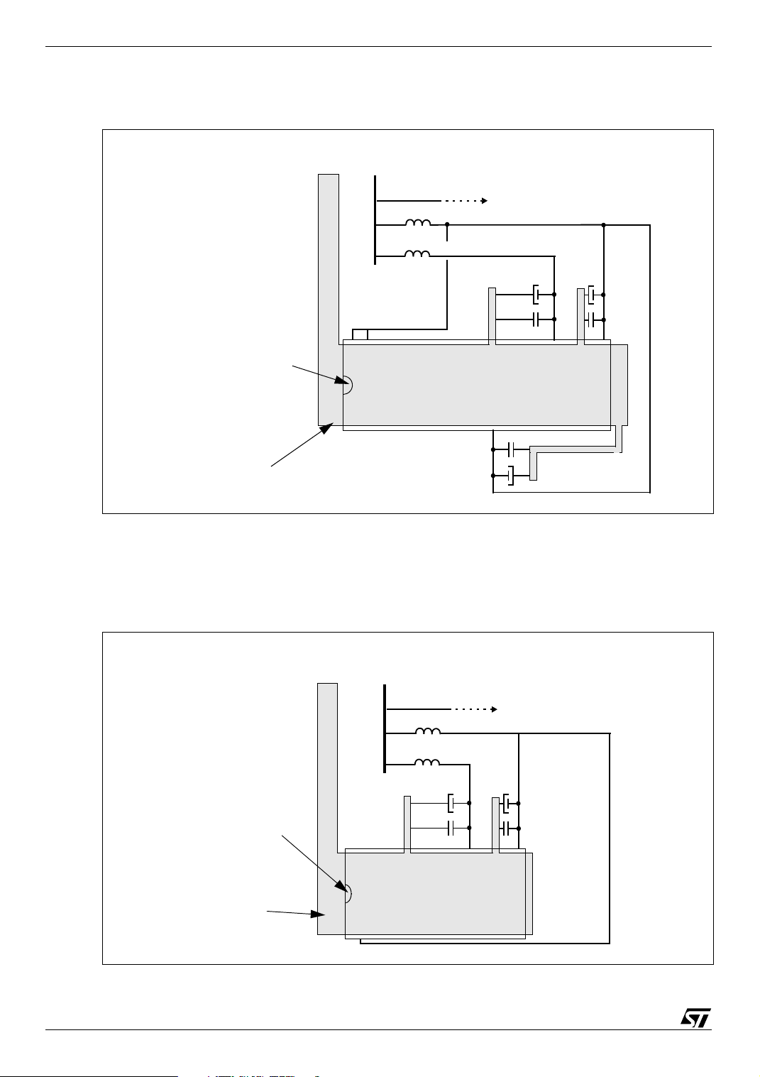
6.1 SDIP56/42 Mounting Instructions
Figure 10 summarizes the neccessary connections between an SDIP56 socket (for ST92x196) and
SDIP42 socket (for ST92186). The schematics is given for a single-layer PCB. It requires 6 straps.
The external filters and the crystal oscillator must be placed as close as possible to the SDIP42
socket (refer to Section 3: External Components for more details).
Please note that all the power and ground pins of the ST92196 SDIP56 package must be connected
even if they are not used in the ST92186 SDIP42 package.
Ground pins VSS1 and VSS2 must be connected as close as possible to each other on the printed
circuit board.
In addition, you MUST connect the following to pins VDD1 or VDD2:
● Pin 56 (VPP) of the ST92196 SDIP56 package
● Pin 55 (TEST0) of the ST92196 SDIP56 package
In order no to overload the drawing in Figure 10, only the 2 socket positions are shown.
10/15
Page 11

Obsolete Product(s) - Obsolete Product(s) Obsolete Product(s) - Obsolete Product(s)
AN2122 PCB Compatibility between ST92196 and ST92186 MCUs
The rules described in Section 1: Ground Plane and Power Supply Lines and Section 3: External
Components must be applied.
Note: You do not need to use all the I/O pins in your software. It is advised not to use, if possible, the I/O
pins that lead to “long” connections between the SDIP56 socket and the SDIP42 socket, such as
P5.5, P5.6, P2.4, P2.5, P2.6, and P2.7. The PCB layout will be better as far as noise immunity is
concerned.
Figure 10: Suggested SDIP56/SDIP42 Schematic Diagram
1
SDIP42 socket
3
5
7
9
11
13
15
17
19
21
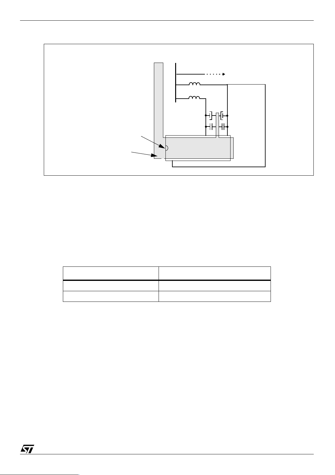
6.2 SDIP56/32 Mounting instructions
1
3
5
7
42
9
40
11
38
13
36
15
34
17
32
19
30
21
28
23
26
25
24
27
22
56
54
52
50
48
46
44
42
40
38
36
34
32
30
SDIP56 socket
Figure 11 summarizes the neccessary connections between the SDIP56 socket (for ST92x196) and
the SDIP32 socket (for ST92186). The schematic is given for a single- layer PCB. It requires 6
straps.
The external filters and the crystal oscillator must be placed as close as possible to the SDIP32
socket (refer to Section 3: External Components chapter for more details).
Please note that all the power and ground pin of the ST92196 SDIP56 package must be connected
even if they are not used in the ST92186 SDIP32 package.
In addition to this, you MUST connect to VDD1 or VDD2 the following pins :
● Pin 56 (VPP) of the ST92196 SDIP56 package
● Pin 55 (TEST0) of the ST92196 SDIP56 package
In order not to overload the drawing in Figure 10, only the 2 socket positions are shown.
11/15
Page 12

Obsolete Product(s) - Obsolete Product(s) Obsolete Product(s) - Obsolete Product(s)
Developing Applications for ST92186 using ST92x196 AN2122
The rules described in Section 1: Ground Plane and Power Supply Lines and Section 3: External
Components must be applied.
Note: You do not need to use all the I/O pins in your software. It is advised not to use, if possible, the I/O
pins that lead to “long” connections between the SDIP56 socket and the SDIP32 socket, such as
P5.0, P2.4, P2.5, P2.6, P2.7, P0.3, and P0.4. The PCB layout will be better as far as noise immunity
is concerned.
Figure 11: Suggested SDIP56/SDIP32 Schematic Diagram
SDIP32 socket
1
3
5
7
9
11
1
3
5
7
9
11
13
15
32
13
30
15
28
17
19
26
24
21
22
23
20
25
18
27
56
54
52
50
48
46
44
42
40
38
36
34
32
30
SDIP56 socket
7 Developing Applications for ST92186 using ST92x196
To avoid problems with your final ST92186 ROMed code, you must follow a few rules when
developing your software:
● Configure your software scriptfile (application_name.scr), makefile (makefile), and emulator
configuration file (hardware.gdb) as if you were using the ST92186 with 32K or 24K of ROM
12/15
(depending on your device), 640 bytes of RAM, and 256 bytes of OSDRAM.
● Only use the cells available in the ST92186.
● Only use the pins available in ST92186 (check the cells present on both the ST92x196 and
ST92186, and for which not all I/Os or alternate functions are implemented on the ST92186).
● DO NOT USE THE OSD MOUSE feature.
● As some I/Os are not bounded on the SDIP32 package, you must configure P2.1, P2.2, P3.1,
P3.5, P3.7, P5.1, P5.2, P5.5, and P5.6 as OUTPUT Push-Pull at the very first beginning of
Page 13

Obsolete Product(s) - Obsolete Product(s) Obsolete Product(s) - Obsolete Product(s)
AN2122 Developing Applications for ST92186 using ST92x196
your software, and NEVER CHANGE THIS CONFIGURATION after initialization. This will
prevent undesired software behavior.
A detailed comparison of the ST92186 and ST92196 packages is given below.
Table 2: Summary of ST92186/ST92196 Differences
Cell Name ST92186 SDIP32 ST92186 SDIP42 ST92x196x SDIP56
ROM 0x00000 to 0x07FFF (32K)
0x00000 to 0x05FFF (24K)
RAM
0x20F000 to 0x20F27F (640
OSDRAM 0x220000 to 0x2200FF (256
External
Interrupts
I/O ports 17 I/Os available :
OSD NO MOUSE
up to 1024 characters in 9x13
up to 256 characters in 18x26
256 bytes of OSDRAM
bytes)
bytes)
1 NMI + 6 external ITs
(INT[7,5:4,2:0])
P0[4:3]
P2[7:3,0]
P3[6,4,2,0]
P4[7:6,1:0]
P5[0]
Translucency output
0x00000 to 0x07FFF (32K)
0x00000 to 0x05FFF (24K)
0x20F000 to 0x20F27F (640
bytes)
0x220000 to 0x2200FF (256
bytes)
1 NMI + 8 external ITs
(INT[7:0])
26 I/Os available :
P0[4:3]
P2[7:0]
P3[7:4,2:0]
P4[7:6,1:0]
P5[6:5,2:0]
NO MOUSE
up to 1024 characters in 9x13
up to 256 characters in 18x26
256 bytes of OSDRAM
Translucency output
0x00000 to 0x1FFFF (128K)
0x20F000 to 0x20FFFF
(4K on ST92x196A)
0x20F000 to 0x20FBFF
(3K on ST92x196B)
0x220000 to 0x22017F (384
bytes)
1 NMI + 8 external ITs
(INT[7:0])
37 I/Os available :
P0[7:0]
P2[7:0]
P3[7:0]
P4[7:0]
P5[6:5,2:0]
MOUSE
up to 1536 characters in 9x13
up to 384characters in 18x26
384 bytes of OSDRAM
Translucency output
IR Preprocessor Available Available Available
Watchdog /
Timer
Standard Timer One 16-bit timer with 8-bit
ADC 6-bit accuracy
Voltag e
Synthesis
PWM 8-bit PWM
DMA Not Available Not Available Available
Multifunction
Timer
Closed Caption
Data Slicer
One 16-bit timer with 8-bit
prescaler
prescaler
3 channels (AIN[4:3,0])
External Trigger input
14-bit PWM/BRM
1 output (VSO2)
4 outputs (PWM[7:6,1:0])
Not Available Not Available Available on some devices
Not Available Not Available 1 or 2, depending on the device
One 16-bit timer with 8-bit
prescaler
One 16-bit timer with 8-bit
prescaler
6-bit accuracy
5 channels (AIN[4:0])
External Trigger input
14-bit PWM/BRM
2 outputs (VSO1, VSO2)
8-bit PWM
6 outputs (PWM[7:6,3:0])
One 16-bit timer with 8-bit
prescaler
One 16-bit timer with 8-bit
prescaler
6-bit accuracy
8 channels (AIN[7:0])
External Trigger input
14-bit PWM/BRM
2 outputs (VSO1, VSO2)
8-bit PWM
8 outputs (PWM[7:0])
13/15
Page 14

Obsolete Product(s) - Obsolete Product(s) Obsolete Product(s) - Obsolete Product(s)
Developing Applications for ST92186 using ST92x196 AN2122
Table 2: Summary of ST92186/ST92196 Differences (Continued)
Cell Name ST92186 SDIP32 ST92186 SDIP42 ST92x196x SDIP56
Video Sync
Error Detector
I2C Not Available Not Available Available
SPI Not Available Not Available Available
SCI Not Available Not Available Available on some devices
Not Available Not Available Available
14/15
Page 15

Obsolete Product(s) - Obsolete Product(s) Obsolete Product(s) - Obsolete Product(s)
AN2122 Developing Applications for ST92186 using ST92x196
“The present note which is for guidance only aims at providing customers with information regarding
their products in order for them to save time. as a result, STMicroelectronics shall not be held liable
for any direct, indirect or consequential damages with respect to any claims arising from the content
of such a note and/or the use made by customers of the information contained herein in connexion
with their products.”
Information furnished is believed to be accurate and reliable. However, STMicroelectronics assumes no responsibility for the consequences of use of such information nor for any infringement of
patents or other rights of third parties which may result from its use. No license is granted by implication or otherwise under any patent or patent rights of STMicroelectronics. Specifications mentioned
in this publication are subject to change without notice. This publication supersedes and replaces all information previously supplied. STMicroelectronics products are not authorized for use as critical
components in life support devices or systems without express written approval of STMicroelectronics.
Australia - Belgium - Brazil - Canada - China - Czech Republic - Finland - France - Germany - Hong Kong - India - Israel - Italy
- Japan - Malaysia - Malta - Morocco - Singapore - Spain - Sweden - Switzerland - United Kingdom - United States
The ST logo is a registered trademark of STMicroelectronics
All other names are the property of their respective owners
© 2005 STMicroelectronics - All rights reserved
STMicroelectronics GROUP OF COMPANIES
www.st.com
15/15
 Loading...