

Page 1
AN2099
APPLICATION NOTE
Guidelines for connecting via JTAG protocol to the STR71x
microcontroller
INTRODUCTION
This application note provides guidelines on how to connect a Host debugger to a target
STR71x board via a JTAG protocol converter, taking into account the internal features of the
STR71x microcontroller product family.
This document is targeted for third party tool suppliers or application engineers interested in
connecting to the STR71x using the JTAG connector. For basic references on the JTAG targeted for the ARM core, please refer to the ARM7TDMI Technical Reference manual
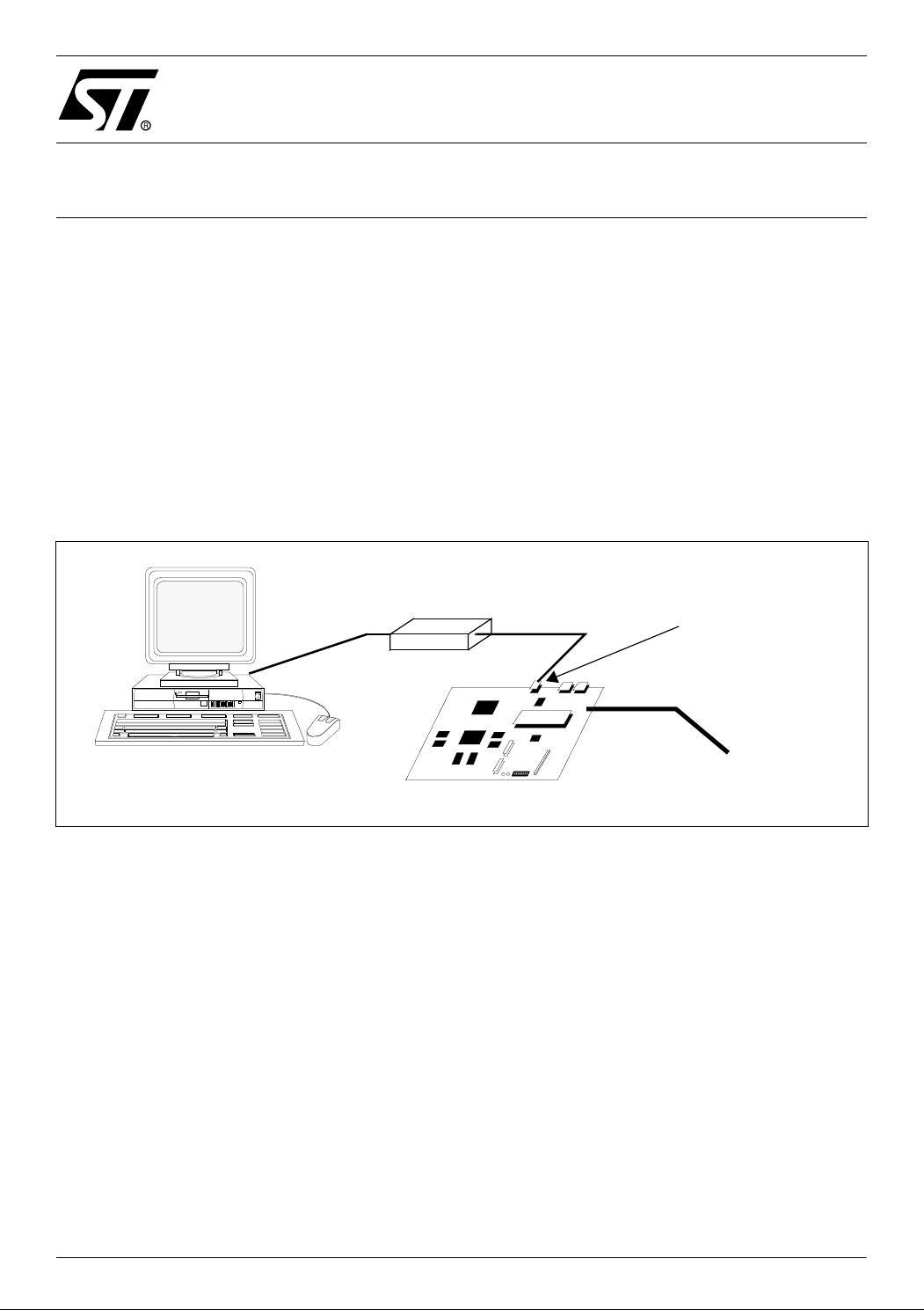
Figure 1. Hardware Setup Example
HOST PC
JTAG protocol converter
STR71x BOARD
JTAG CONNECTOR
POWER
SUPPLY
Rev. 1
AN2099/0405 1/8
1
Page 2

Guidelines for connecting via JTAG protocol to the STR71x microcontroller
1 OVERVIEW
One of the features of the STR71x is to allow the user to boot an application from internal
RAM, which could be used for debugging purposes. However, that system configuration may
potentially result in a hang-up when the debugger attempts to initiate the JTAG communication with the microcontroller. This could be caused by some random code in RAM that could
set the STR71x in an unpredictable mode and prevent JTAG connection to the target.
Section 2 of this application note describes the inherent features of the STR71x affecting the
JTAG connection. Section 3 presents a set of solutions for overcoming all the connection issues. Finally, Section 4, gives a detailed description of the JTAG connection sequence from
the point of view of the JTAG protocol converter.
2 PARAMETERS AFFECTING JTAG CONNECTION
This section covers all the known parameters that affect the JTAG connection.
2.1 DELAY FOR FLASH INITIALIZATION
One aspect to be taken into account is the time for the internal STR71x flash initialization following a system reset. The flash initialization holds an internal signal controlling the ARM
JTAG Reset pin in an undefined state for a deterministic amount of time. This is explained in
detail in section 3.2.
2.2 RESET SIGNALS CONNECTED
Having both system reset and the JTAG reset connected to the same signal will prevent connection since the system reset has to be asserted during the JTAG communication protocol
and released before the start of the application. Therefore having both pins tied to the same
signal will prevent any JTAG communication with the embedded ICE registers.
2.3 PUTTING THE STR71x CPU IN HALT MODE
The Halt Mode of the STR71x CPU is used for debug purposes. This means that once debug
state is initiated, the core is stopped and isolated from the rest of the system until the debugger restores the system state.
The STR71x can only switch to debug state by switching from the main CPU clock (MCLK) to
the ARM JTAG clock (DCLK) controlled by the debugger. The STR71x CPU enters Halt mode
on the next falling edge of MCLK after DBGRQ is asserted. Therefore MCLK has to be running
internally to be able to connect via JTAG. For this reason, it is not possible to connect via
JTAG when the STR71x is in WFI (Wait For Interrupt) mode or STOP mode.
2/8
Page 3

Guidelines for connecting via JTAG protocol to the STR71x microcontroller
2.4 CONNECTION SEQUENCE FROM STANDBY MODE
When the core is in Standby, the core and peripherals are powered down, therefore a straight
connection to the JTAG is not possible if the wakeup logic or system reset has not been triggered. To exit Standby, the wakeup sequence needs to be run to switch the main voltage regulator (which supplies the core and on-chip peripherals) back on to its nominal value. The
wakeup procedure triggers a system reset sequence.
2.5 CONNECTION WHEN CODE IS EXECUTING FROM STR71x MEMORY
Attempting to connect while the STR71x is executing code from its memory is not recommended as this is not considered as a robust solution. For example, the target could have already executed the code to put the STR71x in Standby mode and therefore any subsequent
attempt might fail.
3 CONNECTION METHODS
3.1 BOOT FROM FLASH, COPY TO RAM
One way to bypass the possibility of hitting a random instruction in RAM that might put the
system in an undefined state is to boot an application from address 0x0 in Flash which then
copies an image to internal RAM and executes from it. This will prevent any illegal or unwanted instruction being hit since the Flash is manufactured with known data contents, and
this is also the case when a flash sector is erased. This eliminates the possibility of hitting a
random code when the application is booted from internal RAM.
3.2 FLASH INITIALIZATION
As mentioned in Section 2, no JTAG connection to the target is possible during the Flash initialization phase, as described in Figure 2. The JTAG_EN signal is asserted and might reset
the ARM TAP.
Taking into account the Flash initialization procedure, the JT AG connection sequence can not
be initiated before phase 3 described in Figure 2.
3/8
Page 4

Guidelines for connecting via JTAG protocol to the STR71x microcontroller
Figure 2. STR71x Reset Sequence
CK
255T
CK
2048T
RSTIN
CK
JTAG_EN
~20µs
16T
CK
RSTARM
MCLK
PHASE
234561
The reset sequence is divided into 6 phases:
1. STR71x RESET: The whole device is under reset.
2. CLOCK STABILIZATION: The CPU and the flash are kept under reset for the internal
clock stabilization.
3&4. FLASH INITIALIZATION: The flash is initialized internally keeping the CPU under
reset.
This period varies as it is clocked by an embedded RC oscillator. The 2048TCK
period is set to allow enough time to the flash to be initialized with f
=16MHz.
CK
5. CLOCK START-UP: MCLK is supplied to the various internal blocks of the device
while CPU and peripherals are kept under reset.
6. USER APPLICATION EXECUTION: The user application is executed from address
0x00000000 by the CPU.
3.3 STANDBY PROGRAM
To illustrate the connection sequence in Standby mode, we can use a piece of code, which we
call the Standby program, that puts the core in Standby by setting the PWRDWN bit in the
power control register of the PRCCU. We place this code in internal Flash for execution. This
is the worst case scenario for the debugger connecting to the target since once the CPU starts
to execute the code at address 0x0, the core enters Standby mode.
Therefore this is a perfect test for the JTAG connection sequence since the only way to connect from Standby is to perform a system reset, then after the flash initialization phase (phase
4/8
Page 5

Guidelines for connecting via JTAG protocol to the STR71x microcontroller
3 in Figure 2.) initiate connection before the code starts executing from memory. The debugger should connect before any code is executed from memory, because as seen previously, random code in RAM could result in undefined behaviour by the core. The Standby program is as follows:
*(unsigned short *)0xa0000054 = 0x8000;
*(unsigned short *)0xa0000054 = 0x8040;
for (;;) ;
3.4 CONCLUSION
Connection could be performed as soon as possible:
– after flash initialization
– when MCLK is running internally
– before the code execution starts.
The host debugger should assert DBGRQ after the flash initialization phase and needs to wait
2048 TCK periods before asserting DBGACK, which puts the CPU in Halt mode. This puts the
host debugger in full control of the STR71x CPU before it executes any code from memory.
4 JTAG CONNECTION SEQUENCE EXAMPLE
This section describes the JTAG communication output from the JTAG protocol converter at
the time when the connection is performed on the target. The sequence is analysed from the
first JTAG reset until the system is in debug mode and when the first system accesses are executed by the target, initiated by the debugger. The JTAG communication protocol sequence
is described in chronological order
4.1 TAP IDCODE AND HALT MODE CHECK
This section is optional since it is not a request from the debugger to connect to the CPU , it is
a way for the debugger to identify the CPU by reading back the TAP ID code of the device or
checking whether the device is already in debug mode.
– NJTRST goes out of reset.
– 1 Tck pulse to put the TAP in IDLE.
– TAP is in IDCODE and data is shifted out of TDO This is the first check by the debugger to
identify the device. If the idcode of the device can not be read, the debugger can stop the
connection sequence by displaying a error message in a popup window.
5/8
Page 6

Guidelines for connecting via JTAG protocol to the STR71x microcontroller
– The ICE debug control comms register is read (via scan chain2). This register is read in order
to determine whether the processor or the debugger can write to this register to initiate the
handshaking DBGRQ/DBGACK.
– The ICE debug status register is read to check DBGACK . This is to make sure the core is
not already halted in debug mode.
– DBGACK is set to 1, the system is in debug mode.
– The first instructions are passed to the core via scan chain 1 in debug mode.
– DBGACK is deasserted by writing to the ICE debug control register.
– Read back DBGACK = 0 from the ICE debug status register.
– NJTRST and SYSNRST are asserted, TAP is in RESTART (exit from debug mode).
– SYSNRST is deasserted.
4.2 CONNECTION HANDSHAKE PROTOCOL
This sequence is mandatory for connecting to the STR71x. This section could be executed
after the 2048TCK periods as described in Figure 2. The connection sequence:
– The debugger halts the CPU by asserting DBGRQ internally and waits for DBGACK signal
from the CPU.
– Instructions and data are passed to the core via the Embedded ICE scan chain 1, and the
DBGRQ/DBGACK protocol is controlled via scan chain 2.
– TAP goes to soft reset (TMS=1 for 5 TCK pulses) to make sure the JTAG connection starts
from a reset state
– *Scan chain 2 (to access ICE register) is selected to write to the ICE debug control register:
DBGRQ is asserted to the CPU in order to put the CPU in debug mode. Then the ICE debug
status register is read in a loop until DGBACK is asserted by the CPU. A TAP soft reset is
performed in every loop iteration.
– The status register is read, and DBGACK is asserted, the core has entered debug state. As
described in Section 2.3, the CPU enters Halt mode.
– Once in debug state, the CPU needs to be isolated from the rest of the system so that the
debugger is in full control. System peripherals need to be aware that the core is in debug
state, the core is clocked by DCK instead of MCLK, and all the interrupts to the core are disabled. This is done by forcing bit 0 and bit 2 to logic 1 (DGBACK and INT) in the ICE debug
control register, and reading back the ICE status register to make sure these signals have
been asserted.
– The core In debug state shifts instructions/data using scan chain 1 from which point we can
execute instructions to the core, read/write register values in debug state.
6/8
Page 7

Guidelines for connecting via JTAG protocol to the STR71x microcontroller
4.3 SWITCHING FROM DEBUG TO SYSTEM MODE
This section is not mandatory, but explains when the debugger needs to access the system
memory, this can be done by executing instructions temporarily in RUN mode.
– The ICE debug status register is read via scan chain2 to make sure we are still in debug
mode by checking DBGACK.
– Then switch back to scan chain1. In shifting data and the breakpoint bit into the scan chains,
the brkpt bit value is set to logic “0”
– Then the brkpt bit is set to logic "1" in order to execute an instruction at system speed re-
quested by the debugger, to return to system state ( to access system memory for example
that needs to be performed at system speed). This is done by performing RESTART to exit
debug state to execute the instruction at system speed (MCLK), then goes back to debug
state once the execution has ended (the core is then clocked with DCLK).
– The ICE debug status register is read to make sure the system has changed back to debug
mode by checking DBGACK.
– From which point we can execute instructions to the core in debug state using scan chain1.
7/8
Page 8

Guidelines for connecting via JTAG protocol to the STR71x microcontroller
“THE PRESENT NOTE WHICH IS FOR GUIDANCE ONLY AIMS AT PROVIDING CUSTOMERS WITH INFORMATION
REGARDING THEIR PRODUCTS IN ORDER FOR THEM TO SAVE TIME. AS A RESULT, STMICROELECTRONICS
SHALL NOT BE HELD LIABLE FOR ANY DIRECT, INDIRECT OR CONSEQUENTIAL DAMAGES WITH RESPECT TO
ANY CLAIMS ARISING FROM THE CONTENT OF SUCH A NOTE AND/OR THE USE MADE BY CUSTOMERS OF
THE INFORMATION CONTAINED HEREIN IN CONNECTION WITH THEIR PRODUCTS.”
Information furnished is believed to be accurate and reliable. However, STMicroelectronics assumes no responsibility for the consequences
of use of such information nor for any infringement of patents or other rights of third parties which may result from its use. No license is granted
by implication or otherwise under any patent or patent rights of STMicroelectronics. Specifications mentioned in this publication are subject
to change without notice. This publication supersedes and replaces all information previously supplied. STMicroelectronics products are not
authorized for use as critical components in life support devices or systems without express written approval of STMicroelectronics.
The ST logo is a registered trademark of STMicroelectronics.
All other names are the property of their respective owners
© 2005 STMicroelectronics - All rights reserved
STMicroelectronics group of companies
Australia – Belgium - Brazil - Canada - China – Czech Republic - Finland - France - Germany - Hong Kong - India - Israel - Italy - Japan -
Malaysia - Malta - Morocco - Singapore - Spain - Sweden - Switzerland - United Kingdom - United States of America
www.st.com
8/8
 Loading...