

Page 1
AN2067
Obsolete Product(s) - Obsolete Product(s) Obsolete Product(s) - Obsolete Product(s)
APPLICATION NOTE
VIPower: DIMMABLE WHITE LEDS
POWER SUPPLY WITH VIPer53
In the same way that LED manufacturers succeed
to realize blue LEDs, they now propose white
LEDs inside a monolithic chip, or so called “singlechip white ” LED s .
A current source is the mo re appropriate way to
drive LEDs. For a maximum of flexibility, a large
voltage range must be supported at the output due
to the large threshold of these white LEDs, and the
possible serial arrangement of them.
Furthermore, if these LEDs h av e to be dimmable,
they must be driven with a PWM (current
generator).
As a consequence, key features for this off-line
power supply is a current generator, which can
work as a Pulses Width M odulated mode, with a
wide output voltage range, and must also suite any
input voltage standard, and a galvanic isolation.
1. VIPer53 DESCRI PTION
VIPer53, the first multichip device of the VIPer
family has been chosen to fulfill the requirements.
It f eatures very l ow R
a typical power of 35W in wide range in a standard
DIP-8 package without a heatsink, answering the
of 1Ω allowing to deliver
dson
need for higher efficiency and reduced space
thanks to a lower power dissipation.
1.1. General features
The block diagram is given on Figure 1. An
adjustable oscillator is driving a current controlled
PWM at a fixed switching frequency. The peak
drain current is set for each cycle by the voltage
present on the COMP pin. The useful range of the
COMP pin extends from 0.5V to 4.5V, with a
corresponding drain current range from 0A to 2A.
This COMP pin can be either used as an input
when working in secondary feedback
configuration, or as an output when the internal
error amplifier connected on the VDD pin is
operating in primary feedback to regulate the VDD
voltage to 15V.
The VDD under voltage comparator drives a h igh
voltage startup current source, which is switched
off during the normal operation of the device. This
feature together with the burst mode capability
allows to reach very low level of input power in
standby mode, when the converter is lightly
loaded.
Table 1. White LEDs Power Supply Specification
Parameter Name Conditions Min Typ Max Unit
V
Output current I
Output voltage V
Output Power P
Input Voltage V
OUT
OUT
OUT
IN
= 20V 200 1000 mA
OUT
I
= 1A 5 40 V
OUT
40 W
82 265 V
AC
Rev. 1
1/15November 2004
Page 2

Obsolete Product(s) - Obsolete Product(s) Obsolete Product(s) - Obsolete Product(s)
AN2067 - APPLICATION N OTE
Figure 1. VIPer 5 3 bl oc k diagram
ON/OFF
OVERTEMP.
DETECTOR
OSC DRAIN
OSCILLATOR
PWM
LATCH
S
R1
FF
R2
R3 R4 R5
Q
BLANKING TIME
SELECTION
1V
H
COMP
CURRENT
AMPLIFIER
VDD
8.4/
11.5V
15V
18V
UVLO
COMPAR ATOR
ERROR
AMPLIFIER
OVERVOL TAGE
COMPAR ATOR
0.5V
4.35V
STANDBY
COMPAR ATOR
OVERLOAD
COMPAR ATOR
150/400ns
BLANKING
4V
4.5V
0.5V
PWM
COMPAR ATOR
8V
125k
TOVL COMP SOURCE
converter, the output power is first limited by the
1.2. Overload protection
A threshold of 4.35V typical has been
implemented on the COMP pin. This overload
threshold is 150mV below the clamping voltage of
4.5V which corresponds to the current limitation of
the device. In case of a COMP v oltage exc eedi ng
the overload threshold, the pull up resistor on the
TOVL pin is released and the external capacitor
connected on this pin begins to charge. When
reaching a value of 4V typical, the device stops
switching and remains in this state until the VDD
voltage reaches V
, or resumes normal
DDoff
operation if the COM P voltage returns t o a value
below the overload threshold.
The drain current that the device is able to deliver
without triggering the overload threshold is called
“current capability”, specified as I
in the data
Dmax
sheet. This value must be used to size correctly
the converter versus its max imum output power.
When an overload occurs on secondary side of the
current limitation of the device. If this overload is
lasting for more than a time constant defined by a
capacitor connected on the TOVL pin, the device
is reset, and a new restarting sequence is initiated
by turning on the startup current source. The
capacitors on the VDD pin and on the TOVL pin
will be defined together in order to insure a correct
startup and a low res tart d uty cycle in ov erload or
short circuit operation. Here are the typical
corresponding formulas:
C
C
C
Where t
OVL
VDD
VDD
12.56–×10 tss⋅>
1
84×10
I
>
--------------------------
V
and D
ss
---------------- 1–
D
RST
⋅
DD1tss
DDhyst
are respectively the time
RST
C
⋅
OVLIDDch2
-------------------------------------------⋅⋅>
V
DDhyst
needed for the output voltages to pass from 0V to
2/15
Page 3

Obsolete Product(s) - Obsolete Product(s) Obsolete Product(s) - Obsolete Product(s)
AN2067 - APPLICAT ION NOTE
their nominal values at startup, and the restart duty
cycle in overload or short circuit condition. A
typical value of 10 % is generally set for this last
parameter, as it insures that the output diodes and
the transformer don’t overheat. The other
parameters can be found in the data sheet of the
device.
As the VDD capacitor has to respect two
condition s, the max imu m valu e will b e ret ained to
define its value.
1.3. Stand-by operation
On the opposite load config uration, the converter
is lightly loaded and the COMP voltage is
decreasing until reaching the shutdown threshold
at typically 0.5V. At this point, the switching is
disabled and no more energy is passed on
secondary side. So, the output voltage is
decreasing and the regulation loop is rising again
above the shutdown threshold, thus resuming the
normal switching operation. A burst mode with
pulse skipping is taking place, as long as the
output power is below t he one corresponding to
the minimum turn on of the device. As the COMP
voltage is working around 0.5V, the peak drain
current is very low (it is actually defined by the
minimum turn on time of the d evice, and by the
primary winding of the transformer) and no audible
noise is generated.
In addition, the minimum turn on time depends on
the COMP voltage. Below 1V (V
blanking time increases to 400ns, whereas it is
150ns for higher voltages. The minimum turn on
time resulting from these values are respectively
600ns and 350ns, when taking into account the
internal propagation time. This feature brings the
following benefit:
• This brutal change induces an hysteresis
between normal operation and burs t mode which
is reached sooner when the output power is
decreased.
• A short value in normal operation insures a good
drain current control in case of short circuit on
secondary side.
• A long value in standby operation reinforces the
burst mode by skipping more switching cycles,
thus decreasing switching losses.
More details regarding the stan dby operation c an
be found in the data sheet. See also the prac tical
COMPbl
), the
results obtained in the corresponding section of
this document.
2. WHITE LEDS POWER SUPPLY
2.1. Schematic
The power topology is an off-line fly-back, working
at a fixed frequency of 66KHz.
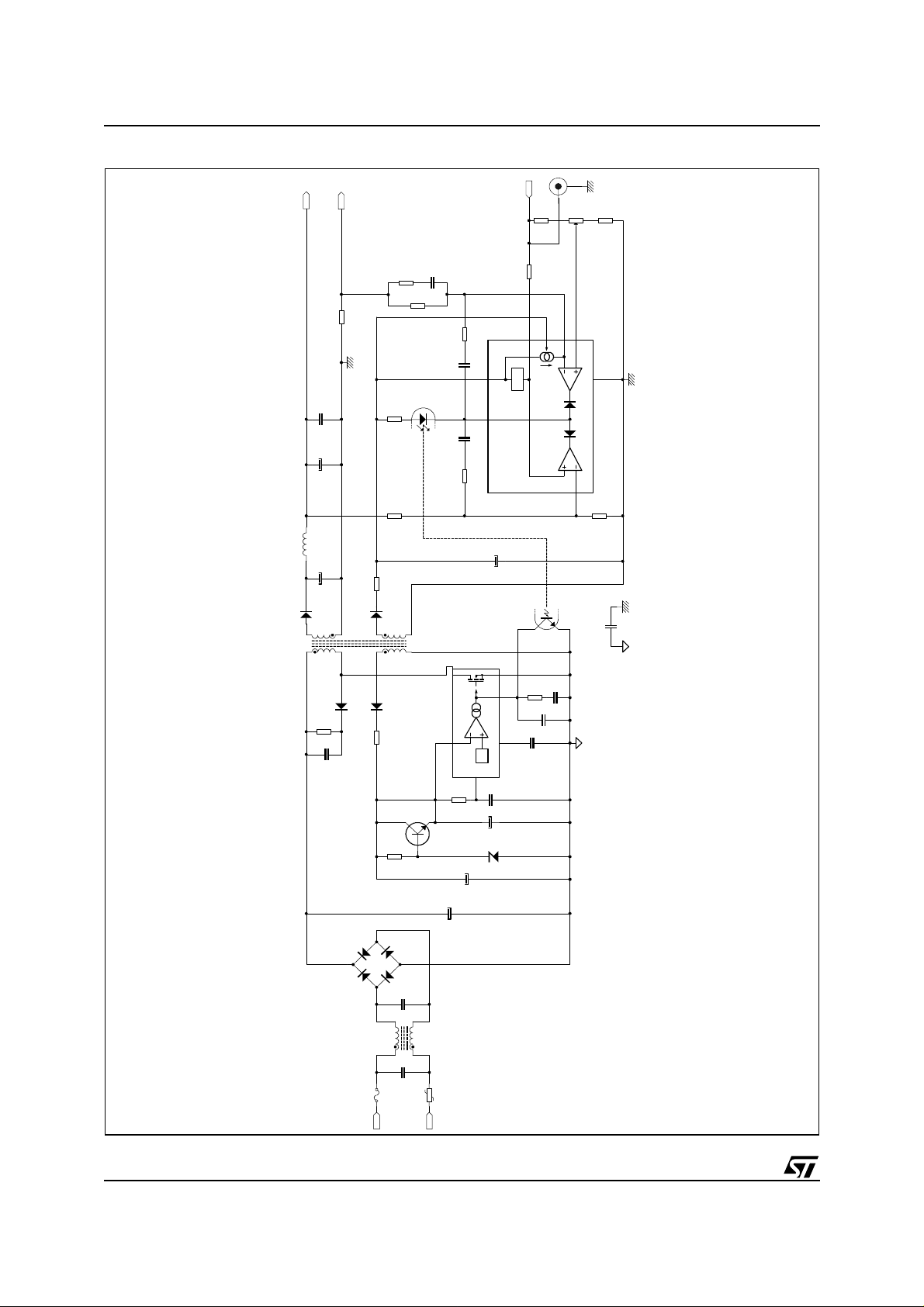
The overall schematic is presented on Figure 2.
2.1.1. Primary section
On the left hand side of the schematic, there is the
fuse F1, inrush current limiter CTN1, input filter T1,
followed by the rectifier BR1 and its bulk
capacitance C3.
R4, C4 and D4 built the RCD clamper, for
discharging the leakage inductance of the
transformer.
D2, R2 and C5 is the rectifier and filtering of the
primary auxiliary winding, used in forward mode
(refer to Section 3). This generates a voltage
supply from 21 V up to 80 V, proportional to turns
ratio between main primary winding and au xiliary
primary winding, and versus input voltage range
(110 V
A serial voltage regulator is required to supply the
VIPer 53 with the correct voltage (around 12 V). It
is built with R14, DZ14, Q1 and C12. Notice that
the V
80 V. This transistor may also dissipate 0.7 W
when input voltage is 250 V
The COMP pin filter is done using C8, R9 and C9.
2.1.2. Transformer
By definition, a current generator may have a large
output voltage variation, according to the output
load.
Then, if auxiliary winding is used in fly-back mode,
there could be a large voltage variation on
auxiliary winding as it is proportional to the
reflected voltage. So, it will be used in forward
mode in order to limit the voltage variation for
supplying the VIPer53.
In order to guaranty the functionality even with low
output voltage load, an auxiliary winding at
secondary side has been added, instead using the
main secondary output to supply the regulation
loop and the voltage limitation (using the
TSM 101). For similar reasons, this auxiliary
winding will be also used in forward mode.
up to 250 VAC).
AC
of this transistor must be higher than
CE0
.
AC
3/15
Page 4
Obsolete Product(s) - Obsolete Product(s) Obsolete Product(s) - Obsolete Product(s)
AN2067 - APPLICATION N OTE
Figure 2. Current Generator Schem at i c
1A OUTPUT
J107
VREF INPUT
P101
1KA
2.2K
R103
0
R107
R131
2.2K
C131
10nF
R101
12K
0.25
R100
6.8K
R107
C113
22nF
C111
100nF
C110
10uF/63V
L101
10µH
C112
220uF/63V
D101
STTH302
R102
680
U2A
C114
100nF
PC817
R108
100K
R106
10K
3.3
R122
D122
BAS21
1K
R109
1
2
345
8
Vref
VCC
GND
6
TSM101
U103
C121
22uF/40V
7
330
R105
U2B
PC817
C_YCAP
2.2nF/2KV
T2
DRAIN
SOURCECOMP
D2
BAS21
D4
EBR44-600
R4
47K/4W
R2
10
C4
1nF/250V
R14
3.3K/0.5W
VIPER53
TOVL
VDD
15V
OSC
C11
4.7nF
R5
5.1K
Q1
2N5550
C12
22uF/25V
DZ14
12V/0.5W
C9
470nF
R9
6.8K
C8
4.7nF
C10
100nF
C5
C3
100uF/400V
1uF/100V
BR1
1A/600V
C2
100nF/400V
T1
COMMON
MODE
F1
0.5A
FILTER
C1
<0
T
C
100nF/400V
CTN1
AC INPUT
4/15
Page 5

Obsolete Product(s) - Obsolete Product(s) Obsolete Product(s) - Obsolete Product(s)
AN2067 - APPLICAT ION NOTE
2.1.3. Secondary section
On the right hand side of the schematic, the
secondary winding is used in fly-back mode.
D101, C112 are respec tively the rectifying di ode
and its filtering. L101 and C110 bui ld another low
pass filter.
The auxiliary sec ondary winding used in forw ard
mode (refer to Section 3) in association with R122,
D122 and C121 built the rectifier and filtering for
the supply of the regulation loop, using a
dedicated component (TSM101). This supply is
independent from the load voltage.
TSM 101 has been design for voltage and current
controller, which can be used for the control of a
current generator, in association with a voltage
limitation. It includes its own reference voltage
(bandgap), and two operational amplifiers.
2.1.4. Current regulation loop
The output current is sensed through the shunt
resistor R100. The shunt voltage is amplified using
R101 and R107 in association with one OPamp of
the TSM 101, building the error amplifier. The
current target is set through the trimmer P101.
R103 and P101 provide a fraction of the reference
voltage provided by the TSM 101 (U103).
There is also another way to set the current target,
using the connector J107 for dimming (see
Section 2.2).
C113 with R107 is the integrator network of this
amplifier, in order to cancel the static error of the
regulation loop.
Then, the regulation loop continue with the opt ocoupler U2 (diode and transistor). This set the
level of the COMP pin filter, which set the peak
drain current VIPer53’s power cell (current control
mode). Thus, the energy stored inside the
transformer during each cycles is transferred on
the secondary side, which supply the output
current.
R131 and C131 is a phase lead net work in order
to compensate the phase delay due to L101/C110
filter, for whole loop stability purpose.
2.2. Dimming
2.2.1. Dimming purpose
The main purpose of this application is to supply
“single-chip white LEDs”, and to dim the
brightness of these LEDs.
Because the white color is obtained from two
peaks in the spectrum (a blue ray and a yellow
ray), there is a dependency between the driving
current and the white color spectrum.
2.2.2. Dimming in the application
This application do not propose any PW M and its
oscillator circuitry, which can be easily found in
dedicated literature. The way to proceed is to
apply an external PWM signal on the node
VREF_INPUT.
Provided that output impedance of the generator is
not higher than 50 Ω, the input voltage is forced by
the external generator instead of the DC reference
voltage of the TSM 101.
The low level voltage of this PWM signal must be
0V, and high level voltage must be around 1 V.
Then, the peak current of the PWM generator can
be set using the trimmer P101, a s in DC mode,
from 0 up to 1 A.
The maximum frequency allowed is limited by
dynamic behavior of the PWM current generator
(refer to Section 2.2.4). The best way to use this
power supply, is to set the lowest frequency
convenient for human eye versus flicker. The
highest the period, the highest the dimming range.
2.2.3. Audible noise
When using the power supply with a P WM signal,
some audible noise may be heard, especially if the
frequency of the external signal is inside the
audible range.
This noise is emitted by the core of the
transformer, and is a normal way to work. This
noise is proportional to the output power
transferred through it.
This noise can be reduced by optimiz ation of the
transformer.
5/15
Page 6

Obsolete Product(s) - Obsolete Product(s) Obsolete Product(s) - Obsolete Product(s)
AN2067 - APPLICATION N OTE
2.2.4. Dynamic behavior of the current
regulation loop
As explain above, the power supply must be ab le
to generates a PWM current, at a sufficient
frequency in order to avoid flicker, with the
possibility to adjust the duty cycle. The shortest
the time response of the regulation loop, the more
linear will be the 0 % up to 100 % characteristics
of the dimming range.
Thanks to the threshold of LED, it is possible to
pulse its current instead to pulse its voltage. Then,
the voltage can be maintained, it a void to charge
and discharged the output capacitances. This
helps a lot for dynamic behavior of the current
generator, since the output filtering capacitance
are quite large.
The dynamic behavior of this current generator is
limited by several root causes in the whole
schematic.
First origin of limitation is the RC couple R101 +
R107 / C113. When the reference level is
changing on the error amplifier (TSM 101-pin 5),
the OPamp must move to this new operating point,
by charging the node TSM 101-pin 3. This is
limited by the charging of the capacitor C113
through the resistor R101 + R107.
Secondly, the filtering c apacitance C121 must be
large enough in order to properly sustain the
supply voltage of the OPamp and the resistor
R102. Effectively, during a transient, the OPamp
has to compensate its output level for loop
stabilization. Then, the dynamic behavior is limited
by the (dis)charging of the capacitor C113 through
the resistor R102, once t he supply voltage of the
amplifier is stable during that transient.
Third, the serial resistance of the load, plus the
shunt resistance R100, and t he serial resistor of
the capacitor C112 are limiting the time res ponse
of the current generator. When switching the
output current from O FF (low current le vel) t o ON
(high current level), the output voltage has to
increase of:
∆Vout ∆I
But, the output current capability will be limited for
a while, until the charging of the capacitance C112
is not completed. When this capacitor is charged,
then the current capability is then available for the
load itself.
outRsloadRshunt
+()⋅=
2.2.5. Voltage limitation
The output voltage limitation is built around R106,
R105, R108, C114 and the corresponding OPamp
of the TSM 101.
R 106, R 105 create a bridge divider of the output
voltage, in order to compare that fraction to the
reference voltage of the TSM 101. The voltage
limit is set by the formula:
R105 R106+
-------------------------------- -
Vout Vref
If the voltage limit is reached, the cable AND of the
TSM 101 allow the voltage limitation circuit to
force the whole loop to reduce the output power.
The stability of the voltage limitation loop i s done
with R108 and C114.
For human body protection against electrical
shocks, this limit has been set to around 40 V, as
advise in safety standards.
2.3. No load operation
The design of the VIPer53 is intended to enter into
burst mode when output see a low load. The
application designer must avoid to en ter in hiccup
mode (or bad burst mode) when no load is
connected.
The resistors R106 and R105 has been designed
in the application in order to have the VIPer53 in
burst mode when no load is connected. A
sufficient current is drawn into R106 and R105,
dissipating the few power transferred to the
secondary side of the transformer during the burst
mode, using the minimum turn-on time (see Figure
7, Figure 9 and Section 4.8, Figure 17 for
measurements).
2.4. Short circuit operatio n
Due to current generator structure, there is no
malfunction or damage when used in short circuit
condition. The current is by definition lim ited. The
output power is low in that condition (refer to
Section 4.8 and Figure 18 for measurements).
2.5. Low Voltage Load
When using very low voltage load (less than 4
volts at output), some instability problem may
appears, depending of t he load ty pe (inductive or
capacitive load, etc.).
⋅=
R105
6/15
Page 7

Obsolete Product(s) - Obsolete Product(s) Obsolete Product(s) - Obsolete Product(s)
AN2067 - APPLICAT ION NOTE
Poles and zeros vary too much, which lead to
make instable the whole transfer function.
This instability may be associated with audible
noise due to some low frequency oscillations. The
user must avoid using loads which have a voltage
below than 4V, in order to ensure a correct
operation of the power supply.
3. Transformer des ign
3.1. Primary Inductance
The primary inductance has been set to 0.5mH,
according to the output power required, and the
(minimum specification of) current capability of the
VIPer53.
The VIPer software helps to define the number of
turns of the primary inductance. It provides a result
of 52 turns, in 2 wires. A diameter of 0.4mm has
been chosen.
3.2. Primary Auxiliary winding
The VIPer53 must be supplied with at least 12.8 V,
for a correct operation. This winding is also used
in forward mode. The turn rat io between primary
winding and primary auxiliary winding according to
the minimum input voltage (100 V
A value of 0.21 will be used with 11 turns on
auxiliary. At maximum input voltage (400 V
auxiliary supply then will be 85 V. This will provide
constraint on the voltage regulator for the VIPer53.
) is 0.18.
DC
DC
), the
3.4. Summary of transformer
Table 2 summarise the spec ification of the power
supply transformer.
4. Measurements
The measurements done on the application board
has been performed at room temperature (27° C),
using an open application board, in still air
condition.
Static measurements have been performed us ing
a programmable electronic load, used as a voltage
generator (so called “static load”).
In order to be as close as possible of the LEDs
load, dynamic measurements have been done
using a discrete voltage generator, as described in
Figure 3 (so called “dynamic load”). This present a
similar load as LEDs according to serial resistance
and parasitic capacitance.
Figure 3. Discrete Voltage Load
3.2.1. Secondary wind in g
The output voltage may vary from 4 V up to 40 V,
and the reflected voltage must n ot exceed 100 V.
The turn ratio should be 0.5 (26 turns) in order to
avoid current mode instability.
A diameter of 0.7mm is provided by VIPer
software.
3.3. Secondary Auxiliary winding
This secondary auxiliary output must guaranty a
voltage from minimum 6 V up to m aximum 32 V
(supply voltage range of the TSM 101). The turn
ratio is 0.077 (4 turns). This provide a supply
voltage from 7.7V up to 30.8 V, which is in line with
the specification of the TSM 101.
4.1. Switching cycle
Figure 4 and Figure 5 show the drain voltage and
drain current respectively in discontinuous mode
and continuous mode, with a 40 Watts static load,
and input voltage respectively at 400 V and 100 V.
Figure 7 and Figure 9 present Drain voltage, Drain
current, V
The output (static) load is 4 Watts (40 Volts,
100 mA), and input voltage is respectively at
100 V and 400 V .
COMP
and V
voltage in burst mode.
OUT
7/15
Page 8

Obsolete Product(s) - Obsolete Product(s) Obsolete Product(s) - Obsolete Product(s)
AN2067 - APPLICATION N OTE
Table 2. Transformer specification
Parameter
Primary inductance Lprim: 0.5mH
Primary auxiliary winding 0.211 11 1 ~0.2 <0.1
Secondary winding 0.5 26 1 0.7 1
Secondary auxiliary winding 0.077 4 1 ~0.2 <0.1
Figure 4. Discontinuous mode (40W/V
Prim. Induct.
or Turn Rati o
Lleak < 4µH (0.8%)
Core: E25H
=400V)
IN
Number
of Turns
52 2 0.4 2.3
Figure 6. Burst mode (P
Number
of Wires
Wire diam.
(mm)
=4W; VIN=100V)
load
Max Current
(A)
Figure 5. Con t in uo us m od e (40 W /V
=100V)
IN
Figure 7. Burst mode (P
=4W; VIN=400V)
load
8/15
Page 9

Obsolete Product(s) - Obsolete Product(s) Obsolete Product(s) - Obsolete Product(s)
AN2067 - APPLICAT ION NOTE
Figure 8. Dynamic response 50% duty cycle at
100Hz
4.2. Dynamic response
4.2.1. Discrete load
An external signal has been applie d on c onne ctor
J107 (node VREF_IN), in order to replace the
static internal reference voltage of the TSM101
with a PWM signal.
The amplitude of this signal is 0 V (low level) - 1 V
(high level) in order to get the full range 0 up to 1 A.
The frequency of this signal is around 100 Hz. The
generator allow to adjust the duty cycle of this
(PWM) signal from 10% up to 90%.
The load used during these measurements is a
discrete load (dynamic load).
Figure 9. Dynamic response 10% duty cycle at
100Hz
Figure 8, Figure 9 and Figure 10 show the
dynamic response of the current generator, when
used in PWM mode, respectively with 50%, 10%
and 90% of duty cycle.
10% and 90% of duty cycle at 100 Hz, is roughly
the minimum and maximum du ty c ycle allowed to
get an acceptable shape for the current pulse.
The minimum turn on/off time is around 1 ms. This
provide a maximum frequency of 500 Hz (2 ms
period).
Figure 10. Dynamic response 90% duty cycle
at 100Hz
4.2.2. LEDs load
Figure 11 and Figure 12 represent the dynamic
response on real load, respectively on 4 white
LEDs, and 1 white LED.
The dynamic response is worst than using discrete
load. It is also worst using 4 LEDs than using 1
LED. This typically shows the LED serial
resistance limitation, as explain below in Section
2.2.4.
The poor dynamic response on LEDs load is
because it has been o ptimized u sing the discrete
load, which have different serial resistance.
There is a room for im provement on LEDs load,
until the signal V
maximum value (4.5V). Poles and zeros may be
tune in order to improve the dynamic response of
COMP
, and then I
V
still do not reach its
COMP
.
OUT
9/15
Page 10

Obsolete Product(s) - Obsolete Product(s) Obsolete Product(s) - Obsolete Product(s)
AN2067 - APPLICATION N OTE
Figure 11. Dynamic response on 4 White LEDs
Figure 12. Dynamic response on 1 White LED
4.4. Load regulation
The regulation versus the load is represented in
Figure 14. The regulation is around 0.4 %.
Figure 14. Lo ad R egulation
1050
1040
1030
1020
1010
1000
990
Iout (mA)
980
970
960
950
010203040
Vout ( V)
4.5. Voltage limitation
Figure 15 is the extension of the load regulation in
Figure 14 (up to the voltage limit). Then, the
voltage limitation act on the output power through
the whole regulation l oop, and the output curren t
then decrease down to 0.
Note: Since the bridge divider has been slightly
tune, the voltage limit may be different than these
measures according to R10 5 and R106 standard
values.
Figure 15. Voltage Limitation
1200
1000
4.3. Line regul a tio n
Figure 13 presents the output current variation
versus AC line input voltage. It shows a variation
of 0.4 %.
Figure 13. AC Li ne R egulation
1050
1040
1030
1020
1010
1000
Iout (mA)
990
980
970
960
950
100 150 200 250 300 350 400
Vin ( V)
800
600
Iout (mA)
400
200
0
0 10203040
Vout (V)
4.6. Power Supply Efficiency
Figure 16 shows the efficiency of the power supply
when output power increases from 0 up to
40 Watts, using several input voltage. Output
voltage vary while output current is 1A.
The efficiency is lower than what could have been
expect for an off line converter. This is mainly due
10/15
Page 11

Obsolete Product(s) - Obsolete Product(s) Obsolete Product(s) - Obsolete Product(s)
AN2067 - APPLICAT ION NOTE
to the current generator structure of this
application, which impose to have the supply of
the VIPer53 connected on a fo rward windi ng, and
because of its associated serial voltage regulator.
Figure 16. Efficiency (I
100.0
90.0
80.0
70.0
n (%)
60.0
50.0
40.0
5.0 10.0 15.0 20.0 25.0 30.0 35.0 40.0
Pout (W )
4.7. Efficiency Vs. output power (V
OUT
=1A)
=100V)
IN
Vin=100V
Vin=200V
Vin=300V
Vin=400V
Main contributors in the power budget are the
transformer, the inrush current limiter, primary and
secondary rectifier, and the clamper.
When output load increase, the ratio between the
dissipated power of these main contributors and
the output power decrease. This is because power
of main contributors is quite cons tant versus the
output load.
Figure 18. In put power in Shor t Circuit mode
3.0
2.5
2.0
1.5
Pin (W)
1.0
0.5
0.0
100 150 200 250 300 350 400
Vin (V)
Figure 19 presents Drain, COMP pin, Output
voltage and Drain current during short circuit
condition. Notice that the converter is in
continuous mode (V
Figure 19. Short circuit con di tio n ( V
=100V).
IN
=100V)
IN
4.8. Extreme load conditions
Figure 17 and Figure 18 show the po wer supply
consumption respectively when no load is
connected at the output and in short circuit
condition.
5. Boa rd description
Figure 17. Input power in No Load mode
1.2
1.0
0.8
0.6
Pin (W)
0.4
0.2
0.0
100 150 200 250 300 350 400
Vin (V)
5.1. Printe d Circuit Board
Figure 20 to Figure 22 present the PCB of the
application. They respectively show all the layers
of the PCB, the BOTTOM layer of the PCB, and
then the TOP OVERLAY layer of the PCB.
11/15
Page 12

Obsolete Product(s) - Obsolete Product(s) Obsolete Product(s) - Obsolete Product(s)
AN2067 - APPLICATION N OTE
Figure 20. All layers (not in scale)
Figure 21. Bottom layer (not in scale)
Figure 22. Top Overlay layer (not in scale)
12/15
Page 13

Obsolete Product(s) - Obsolete Product(s) Obsolete Product(s) - Obsolete Product(s)
AN2067 - APPLICAT ION NOTE
6. Bill of material
The Table 3 presents the bill of material of the
application.
Table 3. Bill Of Material
Symbol Description Quantity
BR1 1A/500V 1
C1 100n/400V 1
C2 100n/400V 1
C3 100u/400V/159 PUL-SI 1
C4 1nF/250V 1
C5 1µF/100V/RLI135 1
C8 4.7nF 1
C9 470nF 1
C10 100nF 1
C11 4.7nF 1
C12 22µF/25V 1
C104 NC 1
C105 NC 1
C107 NC 1
C110 10uF/63V 1
C111 100nF 1
C1 12 220uF/63V/RLI 135 1
C113 22nF 1
C114 100nF 1
C121 22uF/40V 1
C131 10nF 1
COR1 CORNER 1
COR2 CORNER 1
COR3 CORNER 1
COR4 CORNER 1
COR5 CORNER 1
COR6 CORNER 1
CTN1 1
C_YCAP 2.2n/2KV 1
D2 BAS21 1
D4 EBR44-600 1
D101 STTH302 1
D122 BAS21 1
DZ14 12V/0.5W 1
13/15
Page 14

Obsolete Product(s) - Obsolete Product(s) Obsolete Product(s) - Obsolete Product(s)
AN2067 - APPLICATION N OTE
F1 FUSE 1
J1 1
J2 1
J3 1
J101 1
J102 1
J103 1
J107 Vref_in 1
L101 10uH 1
P101 1K 1
P1011 1K 1
Q1 BC546/VCEO=100V/1W 1
R2 10 1
R4
R5
R9
R14
R100
R101
R102
R103
R104
R105
R106
R107
R108
R109
R122
R131
TR1 LN_FILTER 1
TR2 E25 1
U1 STMicroelectronics VIPer53DIP 1
U2 PC817 1
U101 STMicroelectronics TSM1 01A 1
47KΩ/4W
5.1KΩ
6.8KΩ
3.3KΩ/0.5W
0.25Ω
12KΩ
680Ω
2.2KΩ
1Ω
1.8KΩ
56KΩ
6.8KΩ
100KΩ
1KΩ
3.3Ω
1.8KΩ
1
1
1
1
1
1
1
1
1
1
1
1
1
1
1
1
14/15
Page 15

Obsolete Product(s) - Obsolete Product(s) Obsolete Product(s) - Obsolete Product(s)
AN2067 - APPLICAT ION NOTE
Information furnished is believed to be accurate and reliable. However, STMicroelectronics assumes no responsibility for the consequences
of use of such i nformat ion nor for a ny infr ingement of patents or other right s of third par ties whi ch may res ults from its use. No license is
granted by i m plication or otherwise under any patent or pat ent rights o f ST M i croelectronics. Specif i cations mentioned in this public at i on are
subject to change without notice. This publication supersedes and replaces all information previously supplied. STMicroelectronics products
are not authorized for use as critical compone nts in lif e support de vices or syste ms without express wri tt en approval of STMicroelectronics.
The ST logo is a registered trademark of STM i croelectr onics.
All other nam es are the pr operty of their respecti ve owners
Austra l i a - B el gi um - Brazil - Canada - China - Czech Republic - Finland - France - Germa ny - Hong Kong - India - Israel - Italy - Japan -
Malaysi a - M al ta - Morocco - S i ngapore - Spain - Sweden - Switzerland - United Kingdom - Unite d States of Am erica
2004 STMicroelectronics - All rights reserved
STMicroelectronics group of companies
www.st.com
15/15
 Loading...