

AN2064
®
APPLICATION NOTE
Compliance of series/parallel protections for Telecom CO
ST and Cooper Bussmann, experts of wireline networks protection, have jointly prepared this application
note to present a full protection solution based on companion devices from both companies.
Even with all the wireless telecommunication options (GSM, DCS, PCS, UMTS, Wi-Fi, etc…), the wireline
network remains the most cost effective wide range solution to exchange data over the world. The use of
this copper carrier requires system designers to provide adequate protection against overvoltage and
overcurrent events occurring on the line. The goal of this document is to provide telecom system card
designers the necessary information to make proper protection choices.
An example of a wireline telecom network is shown in figure 1. Two different kinds of equipment are connected together by means of a copper line. One line termination is connected to the Central Office (CO)
while the other is connected to the terminal. In the CO, the line goes through the Main Distribution Frame
(MDF), which connects network to the signal cabinet, and is then connected to a subscriber line card.
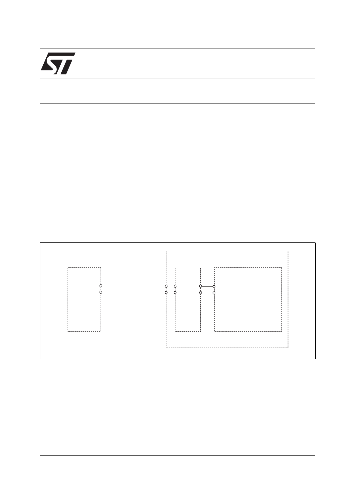
Figure 1: Classical topology of wireline network subscriber line card
Central office
Terminal
The following pages show how to implement the protection stage utilizing series overcurrent protection
devices and Transient Voltage Suppressor (TRISIL™) devices (figure 2). Both elements work together
during surges, TRISIL acts to suppress overvoltages while the series overcurrent devices protect the circuit from lethal overcurrents.
Copper line
MDF
Subscriber line card
TM: TRISIL is a trademark of STMicroelectronics.
REV. 1AN2064/0705
1/14

AN2064 - APPLICATION NOTE
Figure 2: One wire telecom protection topology
Series element
Line side
Transient Voltage Suppressor
or
TRISIL
Protected side
1. TRISIL™ selection
Transient voltage suppressor (TRISIL) selection has to take into account the two working modes it will
meet during its life. The first mode is the normal operating mode where the protection device has to be
transparent, that means no impact on the speech or data signal. The second mode is the suppression
mode where the TRISIL has to eliminate all dangerous transient voltage surges.
During normal operation, we have to focus on voltages and currents managed in the line. These values
depend on the specific countries where equipment is located and the type of signal being managed
(analog or digital). For example, in the US the nominal battery voltage is -56.6V and the ringing voltage
is 150V
, where the normal operating voltage is between 0V and -56.6V in speech or dialing mode and
RMS
between +155.5V and -268.7V in ringing mode. In digital networks the voltages can be the same as those
used in analog networks, as is the case with ADSL. Frequently, ringing is managed by digital code where
only the battery voltage is present (generally -100V), as is the case in ISDN applications. When the
telephone is picked up, the loop current increases and indicates to the CO to stop the ring signal or to wait
for dialing signals. Call connection occurs when the loop current exceeds a few milliamps. Analog CO
systems may use series resistors while digital systems do not. These resistors (10Ω to 100Ω depending
on the applicable country standard) are used to manage line longitudinal balancing while the use of any
series resistance is forbidden in ADSL system. From these requirements we can conclude that the TRISIL
threshold voltage has to be higher than 268.8V for US analog and ADSL networks (190V for Europe) while
the TRISIL leakage current has to be lower than 1mA. The right choice for US is 270V (200V for Europe)
and the leakage current is less than a few µA.
When considering the suppression mode, we have to take into account that telecommunication lines can
be subjected mainly to two kinds of disturbances. The first disturbance is linked to atmospheric effects
while the second disturbance is produced by contact or proximity with the 50/60Hz mains network. These
disturbances are well defined in standards, which can be worldwide or dedicated to a specific country.
2/14
AN2064 - APPLICATION NOTE
The table 1 gives the main lightning standards.
Table 1: Main line card lightning surge standards
Country Standard Surge voltage Waveform Current
Worldwide ITU-T K20 1500V 10/700µs 37.5A
Worldwide IEC-61000-4-5 1000/4000V 10/700µs 25/100A
Worldwide IEC-61000-4-5 1000/4000V 1.2/50µs 25/100A
Germany VDE0433 2000V 10/700µs 50A
Germany VDE0878 2000V 1.2/50µs 50A
USA GR-1089 Core (Telcordia) 2500V 2/10µs 500A
USA GR-1089 Core (Telcordia) 1000V 10/1000µs 100A
France I3124 1000V 0.5/700µs 25A
Main worldwide standards for 50/60Hz overvoltage disturbances can be defined by two parameters: the
applied RMS voltage, between 60V and 1000V, and the test duration, between 0.2s and 15min.
From this section we can conclude that the TRISIL current capability must be adapted according to the
specific country (for example, a waveform surge of 100A for 10/1000µs for the US). As TRISIL are
dedicated to manage high currents for short duration surges (in the range of hundreds of ms) the 50/60Hz
disturbances test requirements show the need of a complementary protection stage, implemented with
series protection devices like fuses or positive temperature coefficient resistors (PTC).
2. Protection circuit
In the protection circuit we find particularities linked to the characteristics already mentioned in the TRISIL
selection section and also linked to the CO line interface. Generally the subscriber line interface circuit
(SLIC) is directly connected to the line without any isolation stage when operating in analog mode, while
in digital applications isolation is achieved using a transformer. Please note that, at the CO side,
protection is split into two areas - the primary protection stage located in the MDF and the secondary
protection directly soldered on the subscriber line card.
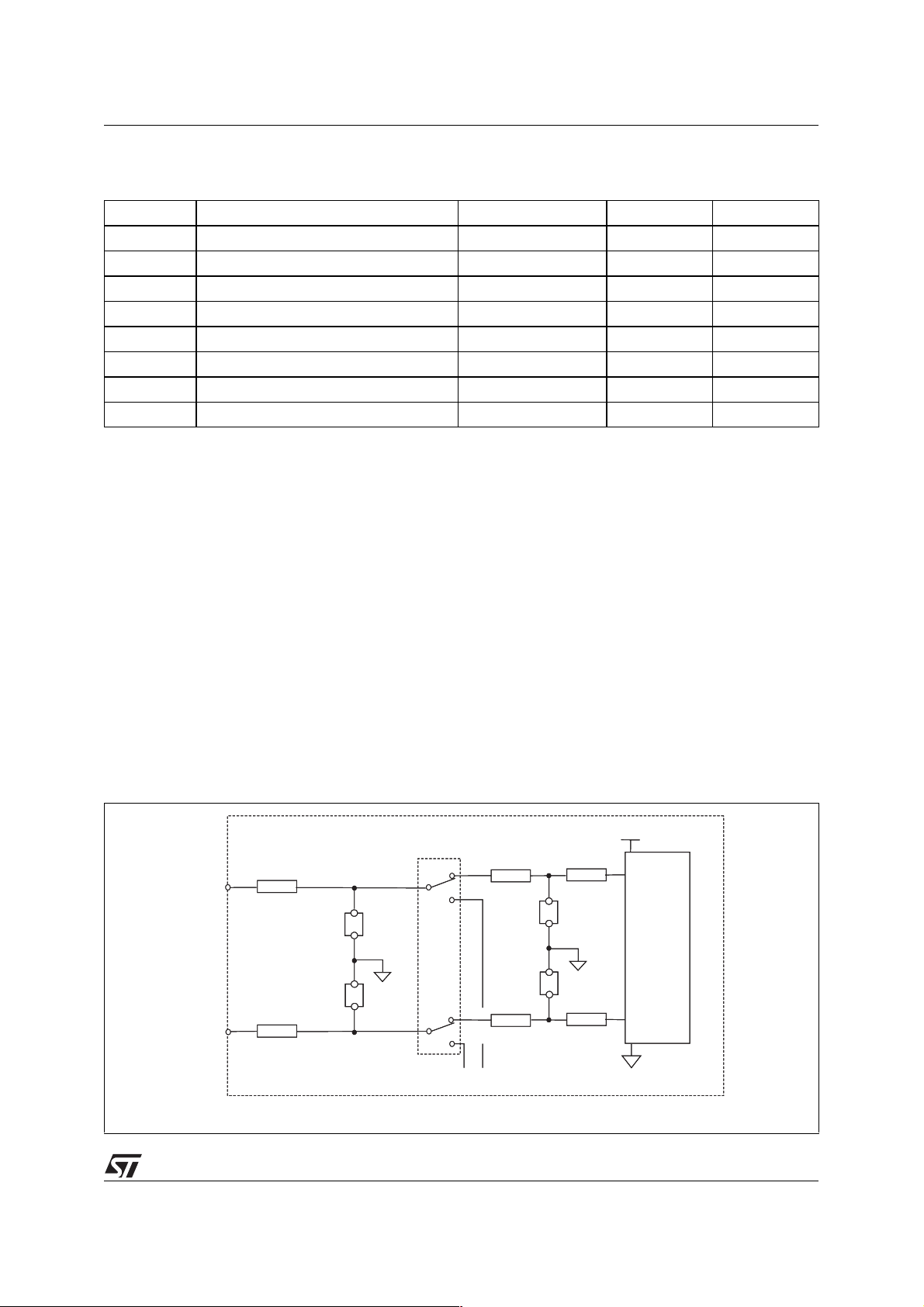
Figure 3: Analog line card protection circuit
-V bat
-
Rs2
Tip
PTC or Fuse
TRISIL 1
Subscriber line card
Relay
Rs1
TRISIL 2
SLIC
PTC or Fuse
TRISIL 1
Ring
Ring generator
Rs1
TRISIL 2
Rs2
Secondary protection, first stage Fuse or PTC andTRISIL 1, second stage TRISIL 2
3/14
AN2064 - APPLICATION NOTE
Figure 3 shows the classical protection topology used to protect one section of an analog subscriber line
card. A first stage uses both series overcurrent protection devices (fuses or PTCs) and TRISIL protectors
(TRISIL 1, threshold voltage = +/- 270V for US) allowing the ring relay to be protected against full lightning
and power contact surges. A second level (TRISIL 2, threshold voltage = 0/-Vbat) allows the SLIC to be
fine tuned protected. The presence of longitudinal series resistors makes the current capability rate of this
TRISIL to be adjusted.
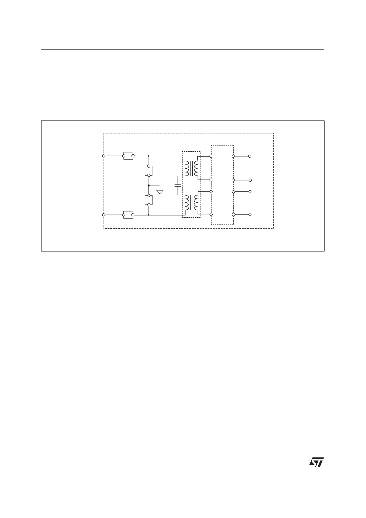
Figure 4: CO ADSL modem protection circuit
ADSL CO Modem
Fuse or PTC
Tip
Ring
Fuse or PTC
Fuse or PTC
TRISIL 1
TRISIL 1
Transformer
C
TRISIL 2
Secondary protection Fuse or PTC and TRANSIL 1
Figure 4 shows the protection topology generally used to protect the ADSL modem (or line cards when
use of a line transformer). This modem is connected to the analog line card by means of a splitter stage
and then receives the same operating voltages. Please note that series resistors are generally not permitted in such an application. Protection is provided by the TRISIL (TRISIL 1, threshold voltage = +/270V), which assumes the full lightning current while the series overcurrent protection devices (fuses or
PTCs) allow the module to be well protected against 50/60Hz power contact.
3. Series protection
As previously mentioned, the use of series overcurrent protection devices is mandatory to protect subscriber line cards against 50/60Hz power contacts. As far as power contact is concerned, standards require the equipment to withstand several tests with different acceptance criteria. First level criterion for
US standards (or A criterion for European requirements) requires the equipment to be fully operational
after tests while second level (or B criterion) allows the system to be out of order but no fire or smoke is
permitted. Table 2 shows AC power fault requirements of the US Telcordia GR1089 standard.
4/14
AN2064 - APPLICATION NOTE
Table 2: Telcordia GR1089 AC power fault test
First Level AC Power Fault Test
Test Applied Voltage, 60Hz Short Circuit Current Duration
RMS
50V
100V
, 400V
1000V
RMS
RMS
RMS
RMS
, 600V
RMS
0.33A 15 minutes
0.17A 15 minutes
1A at 600V 60 Applications, 1 second each
1A 60 Applications, 1 second each
1
2
3
4 (*)
200V
5 NA NA 60 Applications, 5 second each
6
7
8
9 (*)
600V
440V
600V
1000V
RMS
RMS
RMS
RMS
0.5A 30 seconds each
2.2A 5 x 2 seconds each
3A 5 x 1.1 second each
5A 0.5 second each
Second Level AC Power Fault Test
1
120V
2
3
4
(*) Primary protector in place (MDF)
100V
RMS
600V
600V
RMS
, 277V
RMS
RMS
-600V
RMS
RMS
25A 15 minutes
60A 5 seconds
7A 5 seconds
2.2A at 600V 15 minutes
Using series overcurrent protection, two technologies are available, PTCs and fuses.
PTCs are resistive elements that dissipate power when subjected to current, increasing their temperature
and making their resistance quickly increase (10Ω @ 25°C and 100kΩ @ 150°C for example). The nice
feature of the PTCs is that they are resettable but they have two main drawbacks. The first drawback is
its resistance and, as already mentioned, some applications like digital networks do not allow resistive elements. The second drawback is linked to its tolerance, which makes it difficult to achieve line equilibrium
(longitudinal balancing).
Fuses do not have these resistive drawbacks, making them well suited for digital applications.
From the previous discussion we can conclude that the fuse must withstand first level surges for US (or A
criterion for Europe) but may operate for second level surge (or B criterion). As far as the US market is
concerned the fuse has to remain operational for the 10/1000µs 1kV 100A and the 2/10µs 2.5kV 500A
lightning surges. It must also withstand first level AC power faults while it must operate for 277V
and 600V
60A second level AC power faults.
RMS
RMS
25A
5/14

AN2064 - APPLICATION NOTE
4. Example of series / TRISIL protection combination
For this example we will focus on US market applications where low series resistance is an issue. As mentioned earlier, TRISIL characteristics are the following:
. Minimum breakdown voltage > 270V
. Maximum leakage current < few µA
. Current capability > 100A 10/1000µs
. Current capability > 500A 2/10µs
Figure 5: TRISIL choice
Series element
Line side
TRISIL
Protected side
SMP100MC-270
The TRISIL which respects these requirements is the SMP100MC-270 from STMicroelectronics (see figure 5).
Table 3: SMP100MC series datasheet electrical parameters from STMicroelectronics
Types
I
RM
@ V
RM
IR @ V
R
Dynamic
V
BO
max. max. max. max. max. min. typ. typ.
V
BO
Static
@ I
BO
I
H
CC
note1 note 2 note 3 note 4 note 5 note 6
µAVµAV V VmAmApFpF
SMP100MC-120*
108
120 155 150
25 50
SMP100MC-140* 126 140 180 175 25 50
SMP100MC-160 144 160 205 200 25 50
2
5
800 150
SMP100MC-200 180 200 255 250 20 45
SMP100MC-230 207 230 295 285 20 40
SMP100MC-270 2 243 5 270 345 335 800 150 20 40
Note 1: IR measured at VR guarantee VBR min ≥ VR
Note 2: see functional test circuit 1
Note 3: see test circuit 2
Note 4: see functional holding current test circuit 3
Note 5: V
Note 6: V
= 50V bias, V
R
= 2V bias, V
R
RMS
=1V, F=1MHz
RMS
=1V, F=1MHz
* in development
6/14

AN2064 - APPLICATION NOTE
Table 4: SMP100MC series datasheet absolute ratings (T
amb
= 25°C)
Symbol Parameter Value Unit
100
400
140
150
200
400
500
18
9
7
4
20
21
-55 to 150
150
A
A
A
°C
2
s
I
PP
I
FS
I
TSM
I
T
T
T
Note 1: in fail safe mode, the device acts as a short circuit
Repetitive peak pulse current
Fail-safe mode : maximum current (note 1) 8/20 µs 5 kA
Non repetitive surge peak on-state current (sinusoidal)
2
tI2t value for fusing
Storage temperature range
stg
Maximum junction temperature
j
Maximum lead temperature for soldering during 10 s. 260 °C
L
10/1000 µs
8/20 µs
10/560 µs
5/310 µs
10/160 µs
1/20 µs
2/10 µs
t = 0.2 s
t = 1 s
t = 2 s
t = 15 mn
t = 16.6 ms
t = 20 ms
Tables 3 and 4 show that the SMP100MC-270 complies with the CO US market standard requirements.
The telecom system design engineer must next define the suitable fuse. Figure 6 gives the surge
capability limit of the SMP100MC series TRISIL when submitted to the power fault disturbances. The
series overcurrent protection device cannot be a PTC due to its high resistance value, so the only choice
will be the fuse, which meets the following criteria:
. Shall not operate for 100A 10/1000µs surge
. Shall not operate for 500A 2/10µs surge
. Shall operate for 25A
. Shall operate for 60A
Figure 6: I
TSM
and I
(35.4A peak) within 40ms (see SMP100MC series I
RMS
(85A peak) within 4ms (estimated value)
RMS
capability versus surge duration
RMS
Surge Current (A)
70
60
50
40
30
20
10
0
1.E-02 1.E-01 1.E+00 1.E+01 1.E+02 1.E+03
I
TSM
I
RMS
t(s)
F=50Hz
T initial = 25°C
j
curve figure 6)
TSM
7/14

AN2064 - APPLICATION NOTE
Figure 7: Fuse choice
Series element
Line side
TRISIL
Protected side
TCP1.25A
Table 5 gives data about the TCP fuse series from Cooper Bussmann. The TCP1.25A fulfills the Telcordia
10/1000µs and 2/10µs lightning test requirements and the interrupting capabilities with respect to the 25A
and the 60A power cross requests requested by this standard (see figure 7).
Table 5: TCP series datasheet lightning and power cross specification from Cooper Bussmann
LIGHTNING SURGE SPECIFICATIONS
Surge Specification Surge Repetitions
Waveform
(µSec.)
TCP 500mA tested
FCC 47 Part 68 Longitudinal Type B 2 5x320 37.5 N/A Fuse cannot open
FCC 47 Part 68 Metallic Type A 2 10x560 100 800
Surge out 25 10x160 65 N/A Fuse cannot open
TCP 1.25A and TCP2A tested
FCC 47 Part 68 Longitudinal Type A 2 10x160
FCC 47 Part 68 Metallic Type B 2 10x560 100 800 Fuse cannot open
Bellcore GR-1089-CORE First Level Lightning 50 10x1000 100 1000 Fuse cannot open
Bellcore GR-1089-CORE First Level Lightning 50 2x10 500 2500 Fuse cannot open
Surge out 1 10x160 160 N/A Fuse cannot open
Surge out 1 10x560 115 N/A Fuse cannot open
Current
(A)
100 per
fuse
Voltage
(V)
Performance
Requirement
Fuse must open
safely
1500 Fuse cannot open
ELECTRICAL AND POWER CROSS SPECIFICATIONS
Product
Code
Voltage
Rating AC
Interrupting
Rating*
250VAC 600VAC
DC Cold
Resistance**
(ohms)
Typical
Melting
2
I
min. typ. max.
TCP500mA 250 V 50 A 40 A 0.420 0.530 0.640
TCP1.25A 250 V 50 A 60 A 0.070 0.090 0.110
TCP2A 250 V 50 A 60 A 0.050 0.075 0.100
* AC Interrupting Rating (Measured at designated voltage, 100% power factor)
** DC Cold Resistance (Measured at 10% of rated current)
*** On RoHS Compliant Version (-R option)
† Typical Melting I2t (Measured with a battery bank at 60V DC, 10x-rated current, time constant of calibrated circuit less than 50 microseconds)
‡ Typical Voltage Drop (Measured at rated current after temperature stabilizes)
1.3 A
22.2 A
30 A
8/14
Maximum
t†
Clearing
2
s100 A2s
2
s100 A2s
2
s100 A2s
Tot al
Typ ical
Voltage
Alpha Code
Drop‡
Code
471mV F
150mV J
205mV N
Marking
1st
2nd
Code
R***

AN2064 - APPLICATION NOTE
Figure 8 shows the time current curves of the TCP fuse series. This figure is used to verify use of the
TCP1.25A with the SMP100MC-270. For the second level, the fuse has to blow before the TRISIL is damaged, so to verify this point we must compare the I
points of the TCP1.25A. Please note that the I
TSM
given in rms values.
Duration .01s .1s 1s 10s 100s
TCP1.25A
SMP100MC
42A 14.5A 5.5A 3.2A 2.3A
43.1A 17A 9A 4.5A 3A
The comparison of TCP1.25A and SMP100MC datasheet values shows that this solution is convenient for
this application. The next section will refer to test performed on such a module.
Figure 8: TCP1.25A time current curve
points of the SMP100MC with the time current
TSM
points are given in peak values while the TCP curve is
(RMS)
(RMS)
9/14

AN2064 - APPLICATION NOTE
5. US market telecom protection tests
A PCB has been developed according to the criteria established earlier (see figure 9). These boards,
equipped with two fuses TCP1.25A from Cooper Bussmann and two TRISILs SMP100MC-270, have been
tested.
Figure 9: Picture of the developed board
The schematic of these tested boards is given in the figure 10 and performed tests were based on Telcordia (Bellcore) GR1089 for both lightning and power mains disturbances.
. Lightning surge 10/1000µs +/-1kV 100A (25 pulses in each polarity)
. Lightning surge 2/10µs +/-2.5kV and 5kV 500A (10 pulses in each polarity)
. Power mains disturbance 600V 3A 1.1s
. Power mains disturbance 277V 25A 15mn
. Power mains disturbance 600V 60A 5s
Figure 10: Test board diagram
Fuse TCP 1.25A
Tip L
SMP100MC-270
Gnd
SMP100MC-270
Tip S
-
Gnd
-
10/14
Ring L
Fuse TCP 1.25A
Ring S

AN2064 - APPLICATION NOTE
e
e
Figure 11 shows the measurement circuit used for this test series. During lightning and mains contact
tests, the surge current (I surge) injected in Tip L or Ring L (transversal tests) or both Tip L and Ring L
(longitudinal tests) has been measured. The remaining voltages at Tip S or Ring S have been also
measured (V).
Figure 11: Measurement circuit
DUT
DUT
Protected device sid
Protected device sid
V
V
Surge
Surge
Generator
Generator
Current probe
Current probe
I surge
I surge
Line side
Line side
Oscilloscope
Oscilloscope
Voltage probe
Voltage probe
The curves of the figures 12, 13 and 14 show the results, respectively, of :
- a case of lightning test
- a case of first level AC power fault test
- a case of second level AC power fault test.
These curves show no impact of both fuses and TRISIL during first level tests while the fuses open safely
during certain second level tests.
Figure 12: Module behavior during 2/10µs 500A surge test
I surge (100A/div)
V (50V/div)
11/14

AN2064 - APPLICATION NOTE
Figure 13: Module behavior during 600V 3A 1.1s surge test
Figure 14: Module behavior during 600V 60A 5s surge test
I surge (2A/div)
V (100V/div)
I surge (50A/div)
V (100V/div)
Today and for several years to come, wireline networks remain an efficient and cost effective mean to exchange data around the world. The length of these copper lines require system designers to focus on line
interface protection. These protection stages must be in accordance with the standards where equipment
operates. This document has given the philosophy of such a protection and proposes practical results of
tests.
The modules tested were dedicated to US market for CO equipments and were equipped with two
TCP1.25A fuses from Cooper Bussmann and two SMP100MC-270 TRISIL from STMicroelectronics.
Same results have been found with two SMP100LC-270 and two TCP1.25A. The results of these
experiments proved the compliance of this solution with Telcordia (Bellcore) GR1089 standard. The same
approach can be used to protect other kinds of modules (i,e terminal) or CO modules for other countries.
12/14

Table 6: Revision History
Date Revision Description of Changes
11-Jul-2005 1 First issue.
AN2064 - APPLICATION NOTE
13/14

AN2064 - APPLICATION NOTE
The present note which is for guidance only, aims at providing customers with information regarding their
products in order for them to save time. As a result, STMicroelectronics shall not be held liable for any
direct, indirect or consequential damages with respect to any claims arising from the content of such a
note and/or the use made by customers of the information contained herein in connection with their
products.
Information furnished is believed to be accurate and reliable. However, STMicroelectronics assumes no responsibility for the consequences
of use of such information nor for any infringement of patents or other rights of third parties which may result from its use. No license is granted
by implication or otherwise under any patent or patent rights of STMicroelectronics. Specifications mentioned in this publication are subject
to change without notice. This publication supersedes and replaces all information previously supplied. STMicroelectronics products are not
authorized for use as critical components in life support devices or systems without express written approval of STMicroelectronics.
The ST logo is a registered trademark of STMicroelectronics.
All other names are the property of their respective owners
© 2005 STMicroelectronics - All rights reserved
Australia - Belgium - Brazil - Canada - China - Czech Republic - Finland - France - Germany - Hong Kong - India - Israel - Italy - Japan -
Malaysia - Malta - Morocco - Singapore - Spain - Sweden - Switzerland - United Kingdom - United States of America
STMicroelectronics group of companies
www.st.com
14/14
 Loading...