

Page 1
AN2063
Obsolete Product(s) - Obsolete Product(s) Obsolete Product(s) - Obsolete Product(s)
®
- APPLICATION NOTE
VIPower: LOW CONSUMPTION
STAND-BY POWER WITH VIPerX2A FAMILY
GENERAL FEATURES
■ ULTRA LOW STANDBY POWER DISSIPATION
■ BURST MODE OPERATION IN STAND-BY
■ 72% TYPICAL EFFICIENCY
■ CURRENT MODE CONTROLLER
■ OUTPUT SHORT CIRCUIT PROTECTION
■ THERMAL SHUT DOWN PROTECTION
1. INTRODUCTION
The new regulations on t he power supply stand-by consumption f or the battery charger are becoming
more stringent. Thanks to VIPerX2A family low power consumption, it is possible to build a battery
charger with a power consumption in stand-by mode with no-load of 100mW.
In table 1 this charger solution with VIPer12A is presented.
Tab le 1: Operation cond itions
Parameters Limits
Input voltage range 90 to 264VAC
Input frequency range 50-60Hz
Output voltage 5V
Output current 800mA
Output power 4W
Efficiency 72% typical
Line regulation 0.5%
Load regulation 1%
Output ripple voltage 30mVpp
Safety Short circuit protection
2. VIPer12A DESCRIPTION
VIPer12A is a high voltage integrated circuits intended to be used on off line power supply as a primary
side switch. in a monolithic structure housed in DIP-8 or SO-8 package it includes a PWM driver, a
Power MOSFET with 730V breakdown voltage, a start-up c ircuit and several protection c ircuit. It takes
advantage from minimizing the external part count, reducin g the products size and power consum ption.
The application note describes the results obtained when VIPer12A is used in mobile charger
application.
October 2004 1/10
Page 2
Obsolete Product(s) - Obsolete Product(s) Obsolete Product(s) - Obsolete Product(s)
AN2063 - APPLICATION N OTE
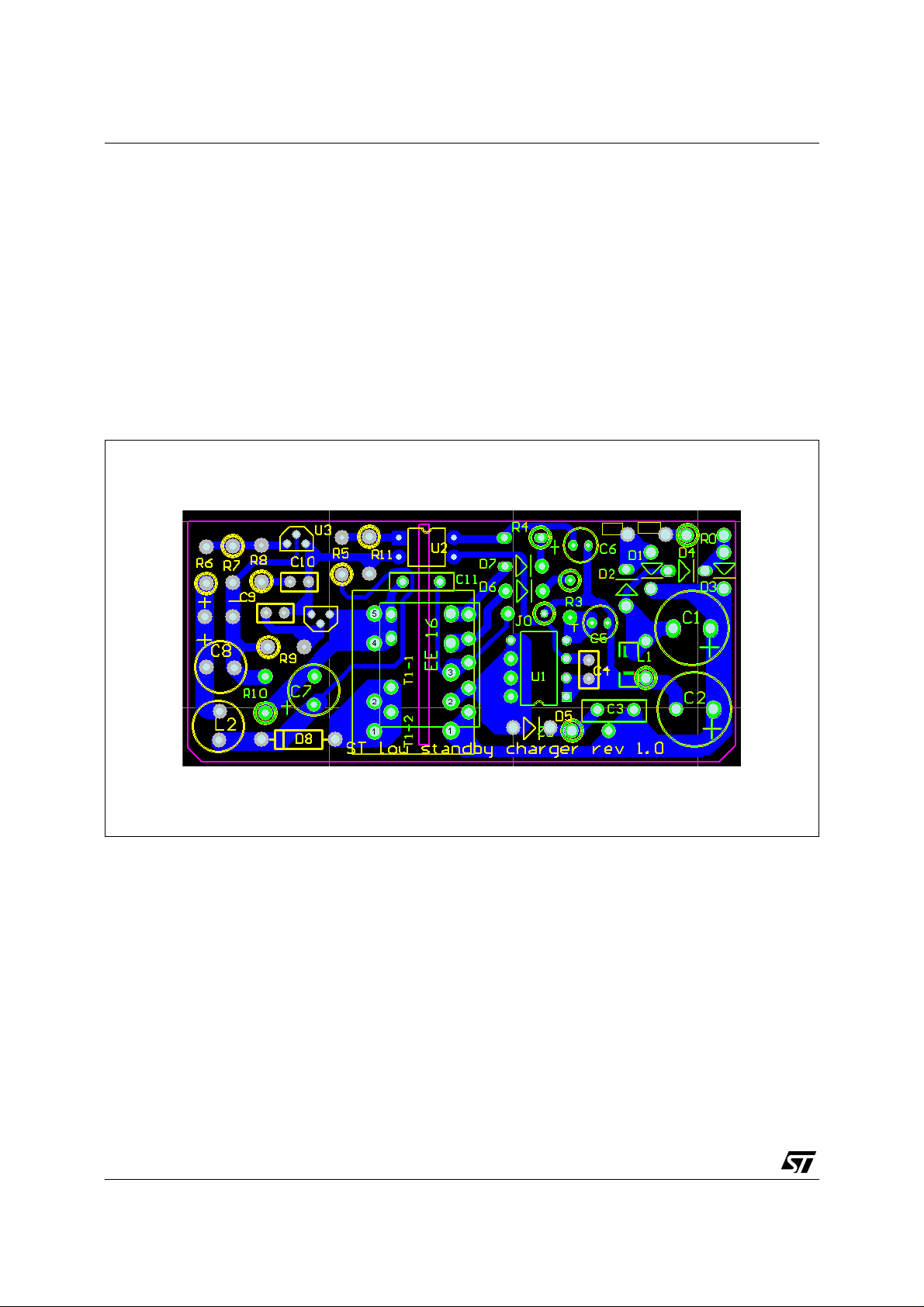
3. PCB LAY-OUT
The layout of the switching power supply is very important in order to minimize noise and interference.
The high switching current loop areas should be kept as small as possible to reduce the radiated
electromagnetic emissions. Figure 1 shows the board layout.
In order to meet safety agencies' requirements, there needs to be an adequate clearance of about 6mm
between the high and low voltage sides of the circuit.
The power grounds need to be separated from the small signal grounds. The current in the power ground
changes very quickly in time; resulting in large transient that induces voltage shifts, which in turn can
disturb critical, sensitive small signal currents. Any disturbance or shift of ground in the small signal
ground will upset c ritical reference pat hs. Therefore, poor g rounding rout ing can ma nifest itself as poor
load regulation, or excessive switching noises on the output.
Figure 1: Demo board bottom foil (not in scale)
4. GENERAL CIRCUIT DESCRIPTION
This board is a fly-back regulator delivering 0.8A at 5V. The AC input is rectified and filtered by the diode
D1, D2, D3, D4, the bulk capacitor C1, and C2 to generate the high voltage DC bus applied to the
primary winding of the transformer, TR1. C1, L1, and C2 provide EMI filtering for the circuit.D9, D10 form
the snubber circuit needed to reduce the leakage spike and voltage ringing on the drain pin of VIPer12A.
The output voltage is reg ulated with a TL431 (U3) via an optocoupler (U2) to the feedback pin. The
output voltage ripple is controlled with the capacitor, C7, with an additional LC PI filter configuration made
up of L2 and C8. It is possible to modify the output voltages by changing the transformer turns ratio and
modifying the resistance values of R6 and R7 in the feedback loop.
2/10
Page 3
Obsolete Product(s) - Obsolete Product(s) Obsolete Product(s) - Obsolete Product(s)
Figure 2: Application schematic
D
AN2063 - APPLICATION N OTE
R0
1N4007
D3
10
1N4007
D1
1N4007
D4
400V
4.7µ
C1
400V
4.7µ
C2
50V
33µ
C5
10µ
33V
C6
47n
C4
PC817
U2
SOURCE
FB
CONTRO L
VDD
1N4148
DRAIN
D7
Opti on E
VIPer12A
U1
1N4007
D2
680µ
L1
Opti on A
1N4148
D6
Opti on C
STTH1L06
D9
P6KE180
D10
R2
0
Opti on B
C111n1kV
TL431
U3
PC817
U2
Opti on E
1.5k
100n
C10
43k
R6
R4
43k
R7
220
R1
0
T1
1N5822
D8
470µ
16V
C7
R3
4.7µ
L2
220µ
10V
C8
C
3/10
Page 4

Obsolete Product(s) - Obsolete Product(s) Obsolete Product(s) - Obsolete Product(s)
AN2063 - APPLICATION N OTE
5. CHARGER APPLICATION
5.1 Schema tic general description
As the total input power dissipation at no load condition of this solution is less than 0.1W, we have to put
our attention to save the power loss es of each c om ponent as m uch as p os sible. Below w e will intr oduce
details for the major approaches which we adopt in this demo board.
5.2 Solutions for energy saving
(A) Losses of VIPer12A controller.
As on this demo board, the power losses of the control part of VIPer12A can be calculated by formula (1).
= Vdd * I
P
viper
Shown in datasheet:
Where:
is the supply voltage of the control part of VIPer12A (range:9V-38V)
- V
dd
- I
is the operation current of the control part of VIPer12A (typical value: 4.5mA)
dd1
The V
is set by considering two ope rative conditions; if we want to save the power of VIPer12A , we
dd
must lower the V
which the required normal operation value of VIPer12A (with 1V margin).
The 10V V
(1)
dd1
value as much as poss ibl e, and at th e sam e time guarant ee t he Vdd higher than 10V
dd
value fixes the suitable turn ratio between secondary and auxiliary winding.
dd
(B) Optimized voltage source for optocoupler.
In a fly-back topology, the voltage source of optocoupler primary side is normally connected to the V
dd
of
the IC directly , but in this board, in order to save energy, another winding is inserted in the transformer for
supplying the optoc ouple r; the voltage supplied with this w indin g is lower than the V
value (typical
dd
value 3V).
(C) Snubber circuit configuration.
An RCD clamp is a popular cheap solution, however it dissipates power even at no load condition: there
is at least a reflected voltage ac ross t he clamp resistor at all t imes. T he p ower l osses on resistor can be
calculated using the formula below:
2
V
R
-----------
R
R
min
is the resistor value; LLK is the leakage inductance; I
min
Where V
is the reflected voltage; R
R
P
peak current limitation value of VIPer12A and f
As at no load condi tion, t he e nergy of ½*L
LK*Ilim*fsw
1
--
L
⋅⋅ ⋅+=
LKIlim
2
is the switching frequency.
sw
can be neglected, then the losses of RCD co uld be
2
f
sw
is the
lim
considered as:
P
R=VR*VR/Rmin
In this case with VR=70V, R
It is possible to save this 60mW power at no load condition using the trans il clamp to replace the RCD
=82KΩ, PR is around 60mW
min
configuration in the snubber circuit.
4/10
Page 5

Obsolete Product(s) - Obsolete Product(s) Obsolete Product(s) - Obsolete Product(s)
AN2063 - APPLICATION N OTE
(D) Optional for the voltage reference devices (TS431 or TL431 or Zener)
The TS431, the TL431 and the Zener can be used as voltage regulators. TS431 shows the low minimum
operation current with the typical value of 150µA. This feature is qu ite useful, because we can remove
the biasing resistor without any voltage regulation performance loss. With this device we can save t he
power losses on the biasing resistor with typical value of 5-8mW.
TL431 is a cost effective solution for the constant voltage. The weakness of this device, in this special
application, is its operation currents is higher than 1mA. In order to get good voltage regulation
performance at full load condition, a bias i ng resistor is a must, but this leads to an add itional power loss.
If the requirement of the perf ormance of out p ut voltage is not so tigh t a zener can be u sed as voltage
reference. The standby power in no load condition is lower than 0.1W with the 3 optional solutions of
voltage reference above. The best solution depends on customers' requirements.
(E) Short circuit the resistors for current limitation on t he auxiliary windings which for V
of VIPer12A and
dd
voltage source for optocoupler primary side.
5.3 Performance Results
5.3.1 Input power consumption at no load condition
Table 2. Stand-by power
Input Power Consumption
V
IN
100Vdc
300Vdc
380Vdc
Note 1 : TL431: 81.7mW; T S431: 77.2mW
I
IN
505µA
252µA
215µA/203µA
81.7mW/77.2mW
P
IN
50.5mW
75.6mW
As shown in table 1, the stand-by power is measured at DC voltage input in order to have more precision
in the input power data. At the high line input of 380Vdc i nput , this de mo board stand by power is around
82mW (with TL431).
Figure 2. Stand-by c on s um p t io n at 38 0V dc in pu t
Primary : 60mW
10mW
10mW
Primary : 60mW
Clamper
Clamper
0 mW
0 mW
1
1
2
2
Secondary : 9mW
Secondary : 9mW
T
T
9
9
7
7
Rectifier diode
Rectifier diode
2mW
2mW
4
4
Swit ch ing lo s ses
Swit ch ing lo s ses
10mW
10mW
Viper12
Viper12
35mW
35mW
Opto coupler
Opto coupler
5mW
5mW
5
5
3
3
Trans for mer lo sses
Trans for mer lo sses
5mW
5mW
Opto
Opto
2mW
2mW
TL431 fo r CV
TL431 fo r CV
3mW
3mW
Biasing Resistor
Biasing Resistor
2mW
2mW
5/10
Page 6

Obsolete Product(s) - Obsolete Product(s) Obsolete Product(s) - Obsolete Product(s)
AN2063 - APPLICATION N OTE
5.3.2 Stand-by operation
Figure 3. V
When no load is applied on secon dary side, VIPer12A works in burst m ode by skipping s ome switching
cycles and this behavior is shown in figure 3. Thanks to this feature, VIPer12A can save a lot of the
switching losses reducing the standby power consumption
& Id at burst mode
ds
5.3.3 Load, Line regulation & Efficiency
Figure 4. Load re g ul a tio n
P$ P$ P$ P$
9GF 9GF 9GF
The output load is changed from 0A to full load 0.8A while the line input voltage is set as 100Vdc,
300Vdc, 380Vdc. The board has a load, line regulation of lower than 1%.
6/10
Page 7

Obsolete Product(s) - Obsolete Product(s) Obsolete Product(s) - Obsolete Product(s)
AN2063 - APPLICATION N OTE
Figure 5. System Efficiency
P$ P$ P$ P$
9GF 9GF 9GF
The measurements are taken at an input voltage of 100Vdc,300Vdc, 380Vdc The typical efficiency
measured is about 73%. Figure 5 shows the efficiency measured when I
from 200mA to maximum value of 800mA.
is set at different values
OUT
5.3.4 Load transient
Figure 6a: Max load → No load Figure 6b: No load → Max load
(50mV / divis i on)
(50mV / div i sion)
As shown in the figures 6a, 6b the maximum overshoot and undershoot value of output voltage are less
than 150mV at transient tests.
7/10
Page 8

Obsolete Product(s) - Obsolete Product(s) Obsolete Product(s) - Obsolete Product(s)
5.3.5 Switching Waveforms of normal operation at full load
1 7 9 4 3
5
P
AN2063 - APPLICATION N OTE
Figure 7: Vds & Id at VIN=100Vdc, P
Figures 7 and 8 show the drain voltage and drain current during normal operation at full load. The power
supply operates in the continu ous current mo de at low line and in discon tinue current m ode at high l ine
input as seen from the waveforms
6. TRANSFORMER SPECIFICATION
=4W Figure 8: Vds & Id at VIN=380Vdc, P
OUT
OUT
=4W
Tab le 3.
Winding description Symbol Number
of Turns
Primary P1 145 0.19mm 2 1 EE-16; Lp=2.5mH at 1V,1KHZ
Secondary S1 11 0.50mm 9 7 Tipple Isolated Wire
Auxiliary1 A1 16 0.10mm 4 5
Auxiliary2 A2 15 0.10mm 5 3
Figure 9. Transformer structure
1
2
9
7
Wire size Start pin End pin Remarks
4
5
3
rimary
Secondary
2
Primary
Secondary
8/10
Page 9

Obsolete Product(s) - Obsolete Product(s) Obsolete Product(s) - Obsolete Product(s)
7. BILL OF MATERIALS
Table 4. Component list
Symbol Part list description Note
C1,C2
C4
C5
C6
C7
C8
C10
C11
R0
R1,R2
R3
R4
R6
R7
D1,D2,D3,D4
D6,D7
D8
D9
D10
L1
L2
T1
U1
U2
U3
AN2063 - APPLICATION N OTE
Elect Cap 4.7µF/400V
47nF/25V
Elect Cap 33µF/25V
Elect Cap 10µF/6.3V
Elect Cap 470µF/16V
Elect Cap 220µF/10V
Film 100nF/50V
Y cap 1nF/1KV
10Ω Fuse
0Ω
220Ω
1.5KΩ TL431:1.5K/TS431:Remove
43KΩ
43KΩ/130KΩ TL431:43K/TS431:130K
1N4007
1N4148
1N5822
STTH1L06
P6KE180
680µH
4.7µH
2.7mH EE-16 Vertical
STMicroelectronics VIPer12A
PC817
TL431/TS431
8. CONCLUSIONS
When the board works in standby, it cons um es less than 0.1W m eeting the "Blue Ange l" Norm. The total
power consumption meas ured a t 100V dc in put with zero load at output is approximately 50mW, while at
380Vdc input this value is about 80mW.
This unit operates in burst mode when the output load is reduced to zero and normal operation is
resumed automatically when the powe r gets back to a level higher than the standby power. The output
voltage remains regulated even when the board operates in burst mode.
9/10
Page 10

Obsolete Product(s) - Obsolete Product(s) Obsolete Product(s) - Obsolete Product(s)
AN2063 - APPLICATION N OTE
Information furnished is believ ed to be accurate and reliable. However, STMicr oelectronics assumes no responsibility for the consequences
of use of such i nformat ion nor f or any infr ingement of patents or other rig hts of third par ties whi ch may res ults from i ts use. No license is
granted by im plication or otherwi se under any pat ent or paten t r i ghts of STMic roelectronics. Specificati ons menti oned in this publication are
subject to change without notice. This publication supersedes and replaces all information previously supplied. STMicroelectronics products
are not authorized for use as critical c om ponents in lif e support de vices or syste m s without express written approval of STMicroelectronics.
The ST logo is a registered trademark of STMic roelectronic s.
All other nam es are the property of th ei r respectiv e owners
2004 STMicroelectronics - All rights reserved
Austra l ia - Belgium - Brazil - Canada - China - Czech Republ i c - Fi nl and - France - Germany - Hong Kong - Ind i a - Israel - Italy - Japan -
Malaysia - Malta - Morocco - Singapor e - Spai n - S weden - Switzerland - Unit ed Kingdom - Uni ted States of Ameri ca
STMicroelectron i cs group of com pani es
www.st.com
10/10
 Loading...