

Page 1

AN2053
Application note
SLIC protection for both classical and new networks
Introduction
Even with booming digital technologies, telecom analog lines remain the most used link in
the world. The market opening to new operators, reserved so far to national telecom
administration, makes an increase of new applications using this simple and cheap way to
supply speech information. POTS (plain old telephone set) is still alive.
Figure 1. Proposed solutions for the subscriber
Central office
Pots
Suscriber house
Pots
Long line
Short line
High speed digital link
Figure 1 shows possibilities subscribers already have got and which will be in a growing
phase in the near future. This will split the SLIC (Subscriber Line Interface Circuit) in two
different types according to the application:
■ The long lines using the classical copper twisted pairs up to several kilometers long
■ The short lines (only a few tens of meter long)
In the second case shown at the bottom of Figure 1, the long distance carrying of the signal
is assumed by modern digital supports like optical fibers, coax, RF link etc.
For both of these applications the protection needs remain one of the major issues of the
system design, so STMicroelectronics, which is one of the major players in the world of
telecom protection, already proposes optimized solutions for these two topologies.
High speed to
Pots coupling
June 2011 Doc ID 10917 Rev 2 1/15
www.st.com
Page 2
Protect against what? AN2053
1 Protect against what?
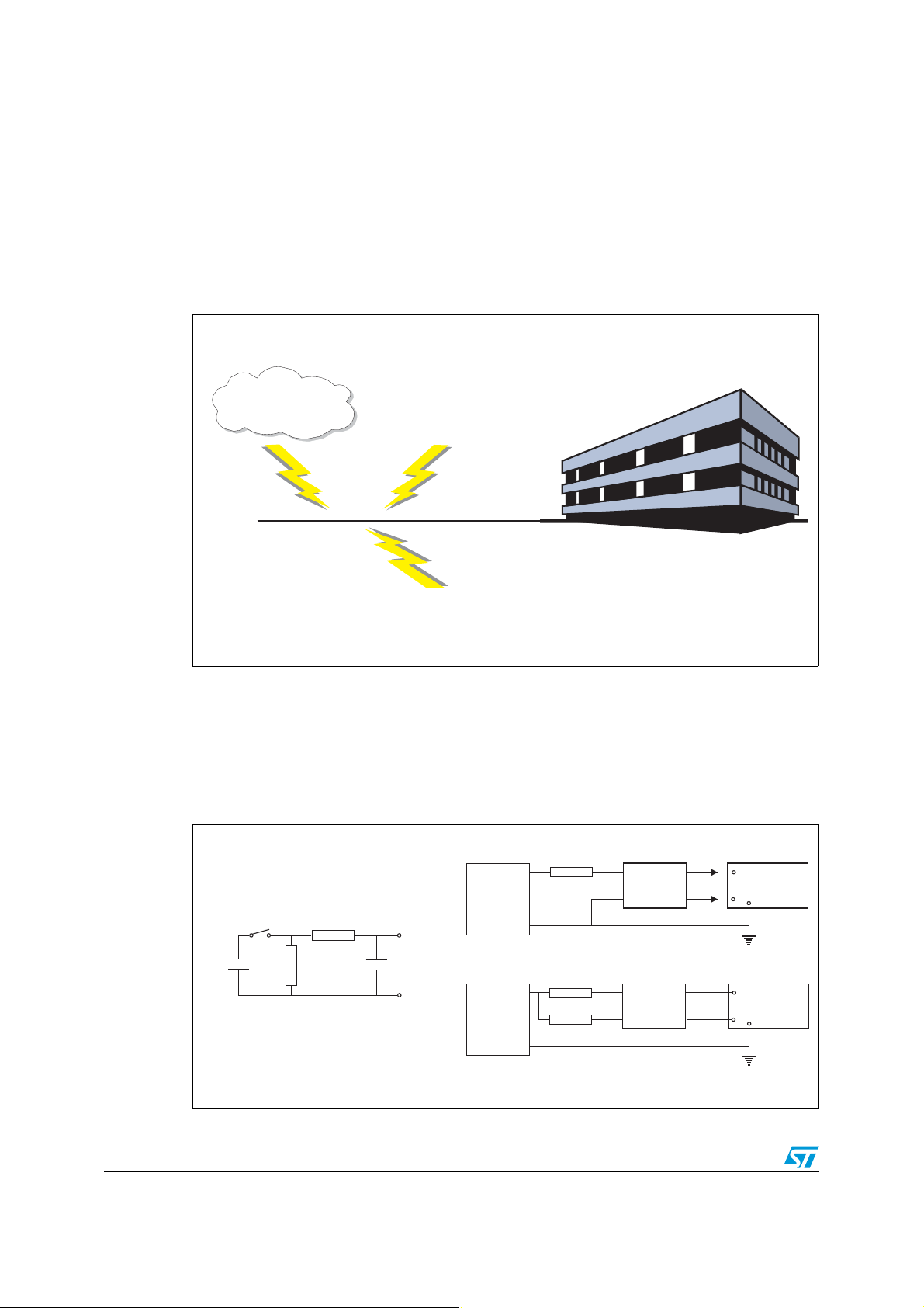
Telecommunication lines are submitted mainly to two kinds of disturbances. The first one is
linked to atmospheric effects while the second one is produced by the 50/60 Hz mains
network (see Figure 2). These disturbances are well defined in individual country standards
and Ta bl e 1 shows the main standards in use.
Figure 2. Main telecom line disturbance causes
Atmospheric effects
Central office
ESD
50/60 Hz mains effects
Figure 3 shows an example of lightning surge definition. This is given by the ITU-T K20
standard (International Telecommunication Union). This simulation is based on the
discharge of a 20 µF capacitance through resistances. The 20 µF capacitance and the 50 Ω
resistance define the surge wave duration while the 15 Ω resistance and the 0.2 µF
capacitance manage the rise time. In this case the surge is defined as a 10/700 µs wave.
The tests shall be managed in both transversal and longitudinal modes.
Figure 3. ITU-T K20 lightning surge test definition
Surge
Surge
Surge
generator
generator
generator
Figure 1
R2 = 15 Ω
Uc
20 µF
R1 = 50 Ω
K20 surge generator
0.2 µF
2/15 Doc ID 10917 Rev 2
Figure 1
Surge
generator
R3 = 25 Ω
K20 transversal test
R4 = 25 Ω
R5 = 25 Ω
K20 longitudinal test
Coupling
Coupling
Coupling
network
network
network
Coupling
network
A
A
A
Equipment
Equipment
Equipment
under test
under test
under test
B
B
B
E
E
E
Equipment
A
under test
B
E
Page 3

AN2053 Protect against what?
Figure 4 shows the ITU-T requirement for both the mains induction and contact test circuits.
This simulation is based on the application of 50/60 Hz through resistance during a
programmed duration (i.e. 0.2 s for induction and 15 min. for contact).
Figure 4. ITU-T K20 power induction and power contact surge test definition
10 Ω
Surge
generator
Uac
Timing circuit
R = 600 Ω
R = 600 Ω
Equipment
A
under test
B
E
Uac
Timing circuit
160 Ω
600Ω
10 Ω
160 Ω
600 Ω
T1
A
S
T2
Equipment
under test
B
E
K20 power induction surge generator
Table 1. Main line card lightning surge standards
Country Standard
Surge
voltage (V)
K20 power contact surge generator
Waveform Current (A)
Worldwide ITU-T K20 1500 10/700 µs 37.5
Worldwide IEC 61000-4-5 1000/4000 10/700 µs 25/100
Worldwide IEC 61000-4-5 1000/4000 1.2/50 µs 25/100
USA GR-1089 Core (Telcordia) 2500 2/10 µs 500
USA GR-1089 Core (Telcordia) 1000 10/1000 µs 100
Table 2. GR-1089 Core Intra-building lightning surge standard
Repetitions
Each
polarity
Test Surge Voltage (V) Waveform
Surge Current per
conductor (A)
1 ±800 2/10 µs 100 1
2 ±1500 2/10 µs 100 1
Ta bl e 1 and 2 show the main worldwide lightning surge standards. Tab l e 1 is dedicated to
classical wired telecom line cards while the Ta bl e 2 is dedicated to intra-building
applications. The main worldwide standards for the 50/60 Hz disturbances can be defined
by 2 parameters: the applied voltage, between 60 to 1000 V and the test duration, between
0.2 s to 15 min. This type of disturbances obliges the designer to put series elements, like
PTC or a fuse between line and protection devices.
Section 2 presents the protection concept used to protect both short and long lines.
Doc ID 10917 Rev 2 3/15
Page 4

LCP concept AN2053
2 LCP concept
Figure 5. LCP15xx concept behavior
Rs1
L 1
GND
-Vbat
Ig
Gate
C
T1
Th1
TIP
D1
ID1
V Tip
GND
Rs2
L 2
RING
V Ring
Figure 5 shows the classical protection circuit using the LCP15xx crowbar concept. This
topology has been developed to protect the new high voltage SLICs. It allows the system to
be programmed for the negative firing threshold while the positive clamping value is fixed at
GND.
When a negative surge occurs on one wire (L1 for example), a current I
flows through the
g
base of the transistor T1 and then injects a current in the gate of the thyristor Th1. Th1 turns
on and all the surge current is short circuited to ground. After the surge, when the current
flowing through Th1 becomes lower than the holding current I
, then Th1 switches off.
h
When a positive surge occurs on one wire (L1 for example) the diode D1 conducts and the
surge current is short circuited to ground.
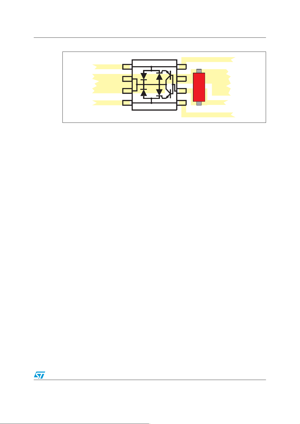
In order to minimize the remaining voltage across the SLIC inputs during the surge, a 4 point
structure has been implemented (Pins 1 and 8 for TIP / Pins 4 and 5 for RING). This fact
allows the board designer to connect the track as designed in Figure 6. With such a PCB
design, extra voltages caused by track stray inductance and current slope (L
) remain
di/dt
located on the line side of the LCP and do not affect its SLIC side.
The capacitor C is used to speed up the crowbar structure firing during the fast negative
surge edges. This allows the dynamic breakover voltage at the SLIC Tip and Ring inputs to
be minimized during fast strikes. Please note that this capacitor is generally present around
the SLIC -V
pin. So to be efficient it has to be moved as close as possible to the LCP15xx
bat
Gate pin and to the reference ground track (or plan) (see Figure 6). Optimized value for C is
220 nF.
4/15 Doc ID 10917 Rev 2
Page 5
AN2053 LCP concept
Figure 6. Example of PCB layout based on LCP15xx protection
To
line side
GND
nF
0
22
To
SLIC side
The series resistors Rs1 an Rs2 designed in Figure 5 represent the fuse resistors or the
PTC which are mandatory to withstand the power contact or the power induction tests
imposed by the different country standards. Taking into account this fact, the actual lightning
surge current flowing through the LCP is equal to:
I
surge
= V
/ (Rg + Rs)
surge
With:
● V
● R
● R
= peak surge voltage imposed by the standard
surge
= series resistor of the surge generator
g
= series resistor of the line card (e.g. PTC)
s
For a line card with 30 Ω of series resistors which has to be qualified under GR-1089 Core
1000 V, 10/1000 µs surge, the actual current through the LCP1521S is:
I
= 1000 / (10 + 30) = 25 A
surge
Doc ID 10917 Rev 2 5/15
Page 6

LCP topology based protection family AN2053
3 LCP topology based protection family
The family of protection systems based on the LCP concept has two kinds of products.
● The LCP15xx protects lines within the range of GND to - V
characteristics given in Figure 5 shows the asymmetry of this protection function. The
V
threshold voltage is programmed by the negative voltage on the gate pin. This
g
voltage is within the range of 0 to -175 V for the LCP1521S
Figure 7. LCP15xx circuit and electrical characteristics
. The electrical
bat
TIP
Vg
G
RING
● The LCPx2-150B1is designed to protect the lines where the normal operating voltage
GND
can be negative as well as positive and located between -V
I
Ih
and +Vb. The electrical
bat
V
characteristics given in Figure 6 show a crowbar adjustable function for both positive
and negative parts of the curve. The knee of the positive part of the curve is
programmed by the voltage on the gate G
programmed by the voltage on the gate G
pin while the knee of the negative part is
p
pin.
n
Figure 8. LCPx2 circuit and electrical characteristics
I
TIP
Gn
GND
RING
Gp
6/15 Doc ID 10917 Rev 2
Vgn
Ih+
Ih-
Vgp
V
Page 7

AN2053 Long line protection
4 Long line protection
The long line concept is used in case of the classic wired telecom network. With this
topology, the core of the system is a huge central office from where many lines connect the
subscribers. In this case the line length can reach several kilometers. This type of subscriber
based on silicon integrated SLIC can be classified in two families:
● With external ring signal management
● With internal ring signal management
The classical one uses a mechanical relay to manage either ring generation or speech
mode.
Figure 9. SLIC with external ring signal management
Tip
PTC or Fuse
Mechanical
relay
(**)
-V bat
(*)
SLIC
PTC or Fuse
Ring
THBTxxx11D
or
TLPxxx
Ring generator
(**)
(**) Used for 100A version
(*) Not mandatoy
Figure 9 shows the protection circuit of a SLIC with mechanical ring relay. The protection
function is implemented in two stages. One is located between the line and the ring relay,
while the other is located between the ring relay and the SLIC.
The first stage, dedicated to the ring generator protection, supports a three-way protection
(THBTxxx11D for 30 A applications or TLPxxx for 100 A requirements). This stage acts
symmetrically at + or - V (For example +/-200 V) where V is chosen as slightly higher than
the maximum ring voltage trip.
The goal of the second stage is to manage a fine protection level in phase with the
requirements of the high integration technology modern SLIC. This stage must switch on for
a voltage higher than the voltage supply of the SLIC.
(*)
LCP1521S
The resistors referenced by (**) allow the LCP15xx to manage both 100 A and 50 A
applications when no resistance is permitted at the PTC or fuse stage. In this case, when a
surge occurs the LCP15xx starts to act and before the current becomes too high in the
LCP15xx, the drop voltage across the resistor (**) allows the TLPxxx device to be fired.
Then all the surge current flows through the TLPxx device.
The resistors referenced (*) are not mandatory and are added when the SLIC to be
protected is very sensitive to the latch up phenomena.
Doc ID 10917 Rev 2 7/15
Page 8

Long line protection AN2053
Figure 10. LCP15xx behavior during 10/700µs negative surge
V tip : 10V/div
I line : 5 A /div
Figure 10 shows both surge current through the TIP pin of a LCP15xx and the voltage
across it when submitted to a 20 A 10/700 µs ITU-T K20 surge. The TIP voltage falls to the
battery voltage (-48 V) and then fires.
Figure 11. LCP15xx behavior during 10/700µs positive surge
I line : 5 A /div
V tip : 1V/div
During a positive surge on TIP wire, the diode between TIP to GND conducts and then all
the surge current flows through the ground. This behavior is shown in Figure 11.
8/15 Doc ID 10917 Rev 2
Page 9

AN2053 Long line protection
Figure 12. LCP15xx behavior during ITU-T K20 power crossing test (600 Ω)
V tip : 20V/div
Is : 200mA/div
Figure 12 shows both voltage across the TIP pin of a LCP15xx and current through it when
submitted to a 230 V
600 Ω power crossing ITU-T K20 surge. The voltage trip at the TIP
rms
pin is roughly between +1 V and the battery voltage (-48 V).
Figure 13. SLIC with internal ring signal management
-V bat
PTC or Fuse
Tip
Line
Ring
+V b
PTC or Fuse
LCPx2-150B1
(*) Not mandatory
In the case of Figure 13 the SLIC is supplied by one positive +V
(*)
SLIC
(*)
+V b
and one negative -V
b
bat
.
This allows the output pins to manage a signal within this voltage range and in particular to
operate in DC biased ring signal mode. For this topology only one protection stage is
needed to perform a fine response when a transient reaches the +V
or -V
b
bat
limit.
The LCPx2-150B1 covers the 30 A 10/1000 µs applications without any series resistance
while it needs series resistance R
(for example PTC) for 50 A applications.
s
Doc ID 10917 Rev 2 9/15
Page 10

Long line protection AN2053
Figure 14. LCPx2-150B1 behavior during GR-1089 Core 10/1000µs +1kV test,
RS = 50 Ω
Vgp : 20V/div
VTip : 20V/div
Is : 5A/div
Figure 15. LCPx2-150B1 behavior during GR-1089 Core 10/1000µs -1kV test,
RS = 50 Ω
Vgn : 20V/div
VTip : 20V/div
Is : 5A/div
Figure 14 and 15 show currents and voltages for the LCPx2-150B1 during both positive and
negative GR-1089 Core 10/1000 µs tests. These measurements were done at ±1 kV on a
board equipped with series resistance RS 50 Ω. For these measurements the positive gate
G
and negative gate Gn are connected to 220 nF speed up capacitors and are respectively
p
biased at + and - 65 V. In such a condition the maximum remaining voltage during the firing
phase is roughly ± 75 V.
10/15 Doc ID 10917 Rev 2
Page 11

AN2053 Long line protection
Figure 16. LCPx2-150B1 behavior during GR-1089 Core first level AC test, 600V,
RS = 50 Ω
VTip : 20V/div
Is : 200mA/div
Figure 16 shows current and voltage waveforms for the LCPx2-150B1.This shows that the
maximum remaining voltage across the TIP or RING line versus ground is roughly equal to
the G
and Gn gate bias voltage ± 65 V.
p
Doc ID 10917 Rev 2 11/15
Page 12

Short line protection AN2053
5 Short line protection
The short line concept is used in case of new telecom networks. This kind of line is linked to
the new applications like WLL, fiber on the corner, NT1+, phone over cable TV network,
telecom by 50/60 Hz supply network etc. Their need for battery voltage as well as the
ringing voltage is lower than those for long line applications. This allows the use of a new
generation of high voltage SLIC circuit which can be either single or double voltage
supplied.
Figure 17. Short line application using high voltage SLIC
-V bat
Tip
PTC or Fuse
(*)
Line
Ring
PTC or Fuse
(*)
LCP1521S
(*) Not mandatory
SLIC
Figure 18. Short line application using SLIC with positive and negative voltages
-V bat
(*)
SLIC
(*)
+V b
Line
Tip
Ring
PTC or Fuse
+V b
PTC or Fuse
LCP02-150B1
(*) Not mandatory
12/15 Doc ID 10917 Rev 2
Page 13

AN2053 Conclusion
6 Conclusion
The telecom deregulation everywhere in the world generated two kinds of line needs. The
long ones are dedicated to the classic telecommunication networks while the short ones are
linked to the emerging remote applications. These quite new systems are based on optic
fiber, WLL, phone over TV network or over 50/60 Hz supply network. For both long and short
line applications, protection is one of the major issues. STMicroelectronics is the major
player in the telecom protection field for both wired and wireless equipment. As far as the
analog telecom lines are concerned, the LCP concept is well adapted to protect SLIC. The
LCP15xx and LCPx2-150B1 cover the protection of all the SLIC of the market.
Doc ID 10917 Rev 2 13/15
Page 14

Revision history AN2053
7 Revision history
Table 3. Document revision history
Date Revision Changes
11-May-2005 1 Initial release.
24-Jun-2011 2 Updated references to standards throughout the document.
14/15 Doc ID 10917 Rev 2
Page 15

AN2053
Please Read Carefully:
Information in this document is provided solely in connection with ST products. STMicroelectronics NV and its subsidiaries (“ST”) reserve the
right to make changes, corrections, modifications or improvements, to this document, and the products and services described herein at any
time, without notice.
All ST products are sold pursuant to ST’s terms and conditions of sale.
Purchasers are solely responsible for the choice, selection and use of the ST products and services described herein, and ST assumes no
liability whatsoever relating to the choice, selection or use of the ST products and services described herein.
No license, express or implied, by estoppel or otherwise, to any intellectual property rights is granted under this document. If any part of this
document refers to any third party products or services it shall not be deemed a license grant by ST for the use of such third party products
or services, or any intellectual property contained therein or considered as a warranty covering the use in any manner whatsoever of such
third party products or services or any intellectual property contained therein.
UNLESS OTHERWISE SET FORTH IN ST’S TERMS AND CONDITIONS OF SALE ST DISCLAIMS ANY EXPRESS OR IMPLIED
WARRANTY WITH RESPECT TO THE USE AND/OR SALE OF ST PRODUCTS INCLUDING WITHOUT LIMITATION IMPLIED
WARRANTIES OF MERCHANTABILITY, FITNESS FOR A PARTICULAR PURPOSE (AND THEIR EQUIVALENTS UNDER THE LAWS
OF ANY JURISDICTION), OR INFRINGEMENT OF ANY PATENT, COPYRIGHT OR OTHER INTELLECTUAL PROPERTY RIGHT.
UNLESS EXPRESSLY APPROVED IN WRITING BY AN AUTHORIZED ST REPRESENTATIVE, ST PRODUCTS ARE NOT
RECOMMENDED, AUTHORIZED OR WARRANTED FOR USE IN MILITARY, AIR CRAFT, SPACE, LIFE SAVING, OR LIFE SUSTAINING
APPLICATIONS, NOR IN PRODUCTS OR SYSTEMS WHERE FAILURE OR MALFUNCTION MAY RESULT IN PERSONAL INJURY,
DEATH, OR SEVERE PROPERTY OR ENVIRONMENTAL DAMAGE. ST PRODUCTS WHICH ARE NOT SPECIFIED AS "AUTOMOTIVE
GRADE" MAY ONLY BE USED IN AUTOMOTIVE APPLICATIONS AT USER’S OWN RISK.
Resale of ST products with provisions different from the statements and/or technical features set forth in this document shall immediately void
any warranty granted by ST for the ST product or service described herein and shall not create or extend in any manner whatsoever, any
liability of ST.
ST and the ST logo are trademarks or registered trademarks of ST in various countries.
Information in this document supersedes and replaces all information previously supplied.
The ST logo is a registered trademark of STMicroelectronics. All other names are the property of their respective owners.
© 2011 STMicroelectronics - All rights reserved
STMicroelectronics group of companies
Australia - Belgium - Brazil - Canada - China - Czech Republic - Finland - France - Germany - Hong Kong - India - Israel - Italy - Japan -
Malaysia - Malta - Morocco - Philippines - Singapore - Spain - Sweden - Switzerland - United Kingdom - United States of America
www.st.com
Doc ID 10917 Rev 2 15/15
 Loading...