

AN2052
Obsolete Product(s) - Obsolete Product(s) Obsolete Product(s) - Obsolete Product(s)
®
- APPLICATION NOTE
VIPower: IMPLEMENTING FREQUENCY MODULATION
ON VIPer53 TO IMPROVE THE EMI EMISSIONS
ABSTRACT
This report describes how the frequency modul ation reduces electroma gnetic interference on an S MPS
using Viper53 as primary PWM-switch.
For your reference, comparison of EMI measurement data will be presented.
1. TEST RESULTS
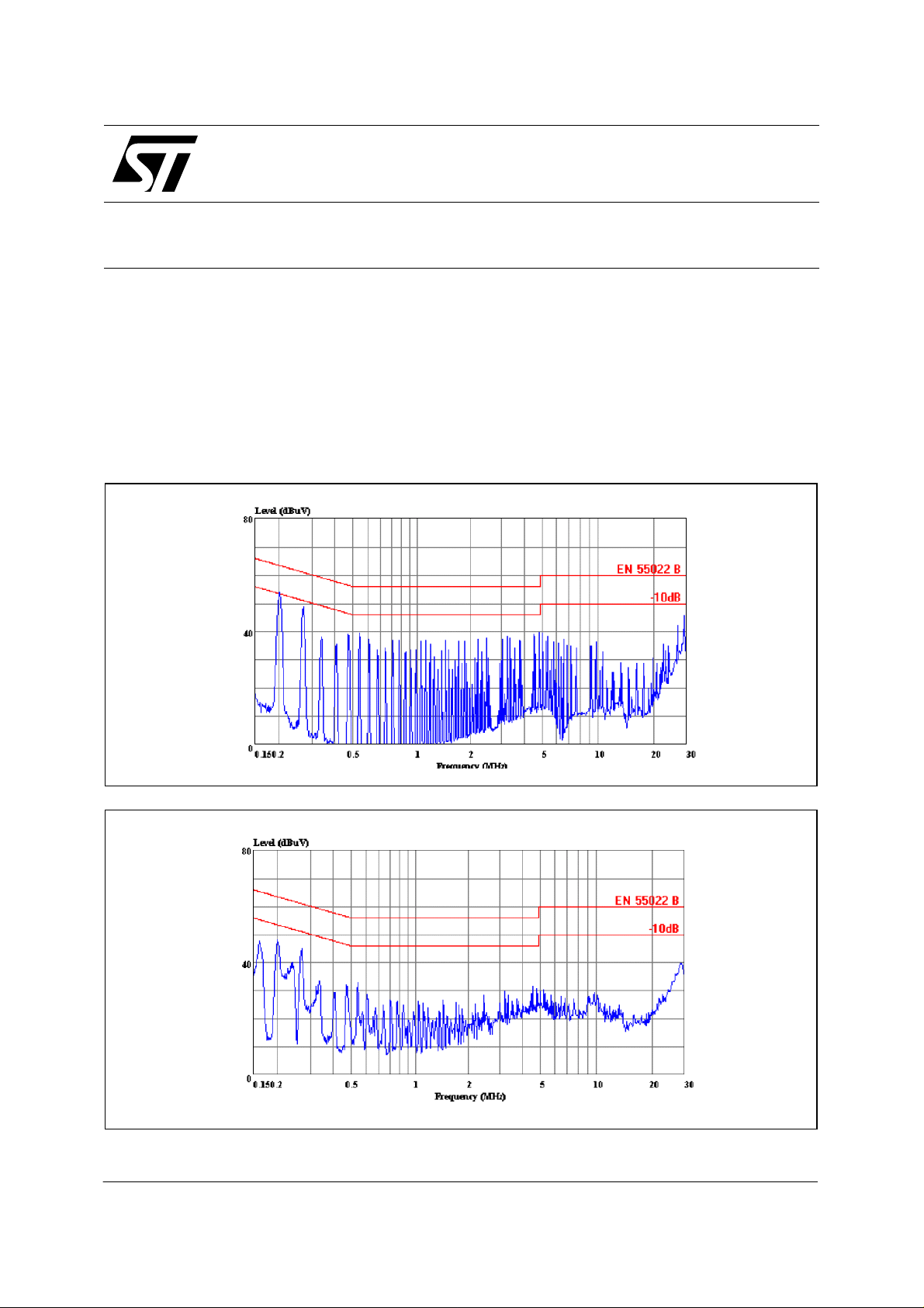
Figure 1: Original, time average at 200kHz, 53.42dBuV / m
Figure 2: FM configuration "A ", time average at 200kHz, 48.07dB uV /m
October 2004 1/7
Obsolete Product(s) - Obsolete Product(s) Obsolete Product(s) - Obsolete Product(s)
AN2052 - APPLICATION N OTE
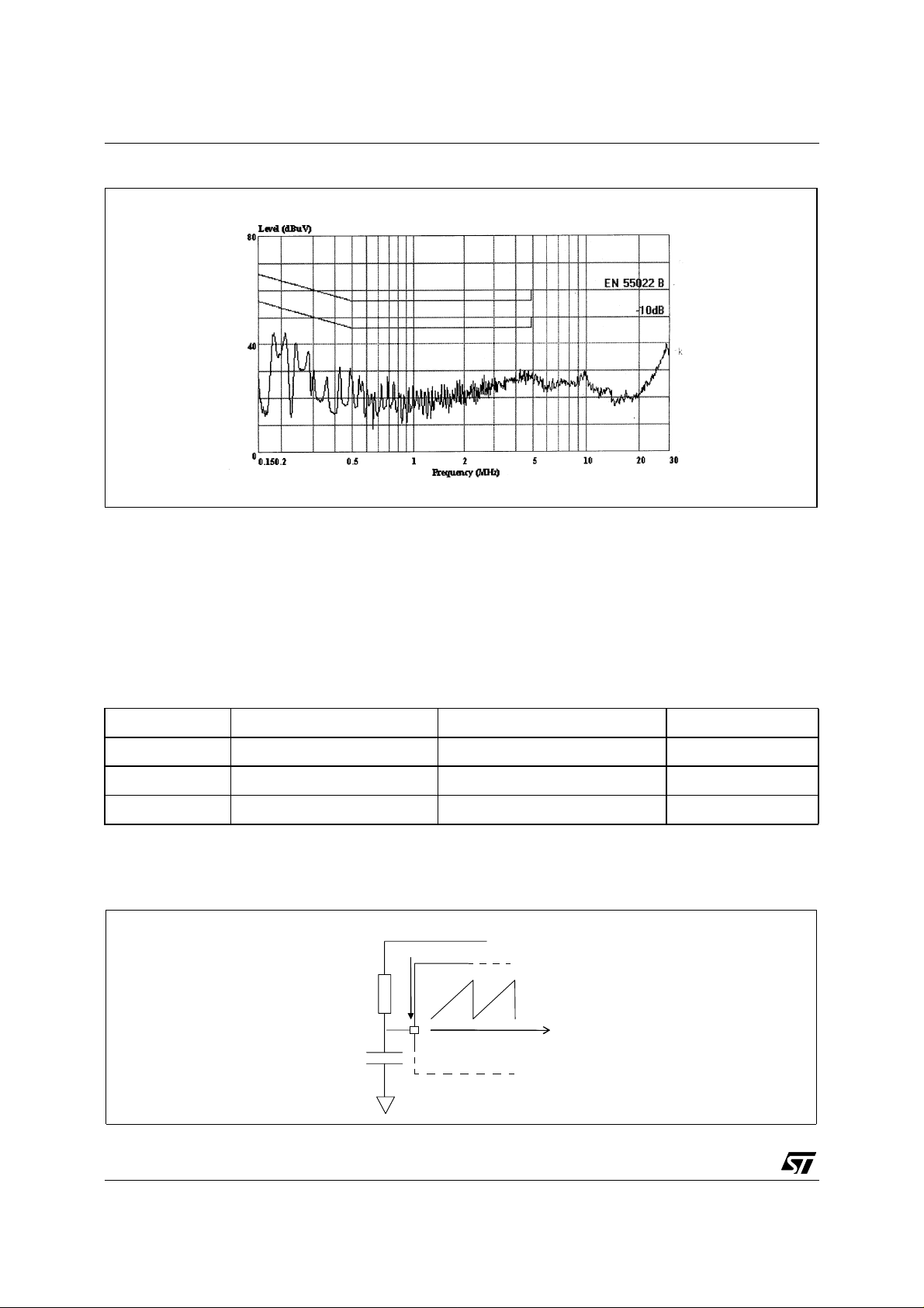
Figure 3: FM configuration "B", time average at 200kHz, 43.92dBuV/m
As shown in figures 1, 2 and 3, using the FM technique a margin improvement will be obtained. At
frequencies lower than 1MHz, the device switching is the primary noise generator. Using the
configuration "A" or "B" a 5 dBuV/m drop is obtained for frequencies lower than 200kHz.
Between 1MHz and 10MHz, both configuration "A" and "B" ma ke a dramatic drop greater than 15dBuV/
m. Above 10MHz, FM technique benefits are reduced and capacitive coupling between copper tra cks in
PCB is dominant.
Tab le 1:
<1MHz 1Mhz ~ 1 0MH z >10MHz
Original Marginally pass Pass Enough margins
“A” Pass More margins Enough margins
“B” More margins More margins Enough margins
2. CIRCUIT AND DESCRIPTION OF TEST CONFIGURATIONS
Figure 4: Original configuration (Fixed frequency at 70 kHz, and no FM).
Vdd=10Vdc
IC1=1mAmax
10k
OSC
VIPer53
2/7

Obsolete Product(s) - Obsolete Product(s) Obsolete Product(s) - Obsolete Product(s)
AN2052 - APPLICATION N OTE
Figure 5: Configuration "A" (Switching frequency from 63kHz to 77kHz FM cycle 20ms, 50Hz).
50Hz
900k
900k
IC1=0.83mA
11k
OSC
Vdd=10V
VIPer53
Figure 6: Configuration "B" (Frequency from 63 kHz to 77 kHz, FM cycle 1.4ms, 700Hz).
V2=10Vpeak
Oscillator
IC1=0.2mA
700Hz
50k
IC1=0.83mA
11k
OSC
V1=10V
VIPer53
Changing the resistor value between Vdd and O SC pin, it is possib le to modify the f requency oscillator
(capacitor value is fixed at 220nF). In this way the FM pe rcentage can be set . The target F M pe rcentage
is +/-10%. In the original ci rcuit a 10kohm resistor is used, obtaining a switching frequency of 70 kHz.
This resistor value gives a charging current capacitor of 1mA max.
The external circuit works in order to increase the switching frequency. Therefore, it is necessary to
change the resistor value between V dd and O S C pin i n order to reduc e m inimum swit ching frequency to
66KHz. As a result the new resistor value will be 11kohm, obtaining a charging current of 0. 9mA when
external voltage is 0V. The switching frequency variation depends on the charging current capacitor,
therefore it is proportional to the external voltage. Maximum value of the switching frequency is 77 kHz: it
is obtained when the charging current is 1.1mA where 0.9mA is given by Vdd and 0.2mA is supplied from
the external circuit.
Below, the design of the resistor value, between OSC pin and the oscillator, is explained:
- in configuration "A", maximum voltage is 374V, so the resistance is R=373V/0.2mA =1.8Mohm ;
- in configuration "B", the maximum voltage is 10V, so the resistance is R=10V/0.2mA =50kohm.
It is important to verify the frequency obtained using the oscilloscope . If necessary this frequency value
will have to be tuned to the desired value.
In figures 7 and 8, the typical clock signal is shown.
3/7

Obsolete Product(s) - Obsolete Product(s) Obsolete Product(s) - Obsolete Product(s)
AN2052 - APPLICATION N OTE
Figure 7: Configuration "A".
AC signal (50Hz oscillato r) PWM ramp signa l
Figure 8: Configuration "B".
Oscillator signal (700Hz os c illa tor) PWM ramp signal
3. ANALYSIS AND POSSIBLE FURTHER DEVELOPMENT
In figures 9, 10 and 11 the peak value data of the three tested configurations are shown.
4/7

Obsolete Product(s) - Obsolete Product(s) Obsolete Product(s) - Obsolete Product(s)
Figure 9: Original peak.
Figure 10: Configuration “A” peak.
AN2052 - APPLICATION N OTE
Figure 11: Configuration “B” peak.
5/7

Obsolete Product(s) - Obsolete Product(s) Obsolete Product(s) - Obsolete Product(s)
AN2052 - APPLICATION N OTE
One remarkable point is that the peak value of the three tested configurations is almost the same.
The major difference between peak and av erage measurement is in the filter and in the measurement
time. Wide band filter and short measurement time are us ed to capture the peak value ; while narrow
band filter and relatively long measurement time are used to capture the average value.
Through web sea rch engines it is possibl e to find the definitions f or the terms "peak" and "ave rage" as
"spectrum peak" and "spectrum average", respectively. These de fin itions are different from the "timepeak" and "time-average" defined in this report.
Instead, the term "frequency modulation" can be found on the web as "spread spectrum",
The spectrum peak i s th e hi ghes t c om ponent over the frequency spectrum. In EMI t es t data of SM PS, it
corresponds to a low frequency.
The spectrum average is the average noise over the whole frequency spectrum.
The time peak is the "peak" data measured by most EMI test lab. Noise, in terms of dBuV/m, is measured
through a wide band filter within a short period of tim e.
Analysing such measurements, the fact that FM does not bring benefit is highlighted. The measurements
obtained are very similar to the spectrum envelope of figure 9.
The time average is the "average" data measured by EMI test lab. Noises are measured through a
narrow band filter, over a relatively long period of time.
Note that there is no regulation on the measurement average time.
4. OPTIMIZATION OF EXTERNAL OSCILLATOR
Targeted to lower down the average value of EMI noise, t he P WM m ust go t hroug h t he who le f requency
range within the testing time. In other words, the FM cycle is as short as poss ible. On the other hand,
since the actual PWM signal is modulated by the FM c ycle and switching cycle, to avoid audible noise,
FM frequency is suggested to be lower than 2 kHz.
This also accounts for the fact that the average data of configuration "B", 700Hz osc illator, is lower than
the configuration "A", 50Hz oscillator.
Another drawback of configuration "A" is the dependency on AC mains, which can be an issue in
transformer design.
5. REFERENCE
Oscillator with 2 BJTs ., low cost and startup volutage down to 3V.
6/7

Obsolete Product(s) - Obsolete Product(s) Obsolete Product(s) - Obsolete Product(s)
AN2052 - APPLICATION N OTE
Information furnished is believ ed to be accurate and reliable. However, STMicr oelectronics assumes no responsibility for the consequences
of use of such i nformat ion nor f or any infr ingement of patents or other rig hts of third par ties whi ch may res ults from i ts use. No license is
granted by im plication or otherwi se under any pat ent or paten t r i ghts of STMic roelectronics. Specificati ons menti oned in this publication are
subject to change without notice. This publication supersedes and replaces all information previously supplied. STMicroelectronics products
are not authorized for use as critical c om ponents in lif e support de vices or syste m s without express written approval of STMicroelectronics.
The ST logo is a registered trademark of STMic roelectronic s.
All other nam es are the property of th ei r respectiv e owners
2004 STMicroelectronics - All rights reserved
Austra l ia - Belgium - Brazil - Canada - China - Czech Republ i c - Fi nl and - France - Germany - Hong Kong - Ind i a - Israel - Italy - Japan -
Malaysia - Malta - Morocco - Singapor e - Spai n - S weden - Switzerland - Unit ed Kingdom - Uni ted States of Ameri ca
STMicroelectron i cs group of com pani es
www.st.com
7/7
 Loading...