

Page 1
AN2042
Application note
VIPower: dimmable driver for high
brightness LEDs with VIPer22A-E
Introduction
This application note introduces an innovative solution to drive high brightness 1W LEDs
(Light Emitting Diode), using VIP e r22A-E in flyback configuration with output current control.
The power supply is able to drive an array of 1 to 8 LEDs in European range, i.e. 185-265
VAC with no modifications. By means of an input voltage doubler, it is possible to use the
same VIPer device also in U.S. input voltage range, guaranteeing the specs. A new control
technique is used to adjust the duty cycle of the ou tput current, in or der to dim the luminosity
of the LEDs down to 10% of the maximum value (patent pending by STMicroelectronics).
The proposed driver can be suitably used in applications such as landscape lighting, street
lighting, car parks, bollards, garden lighting, large area displays and so on.
Also domestic applications such as room lighting, decorative fixtures and architectural
lighting can benefit from the advant age of this dimmable light source.
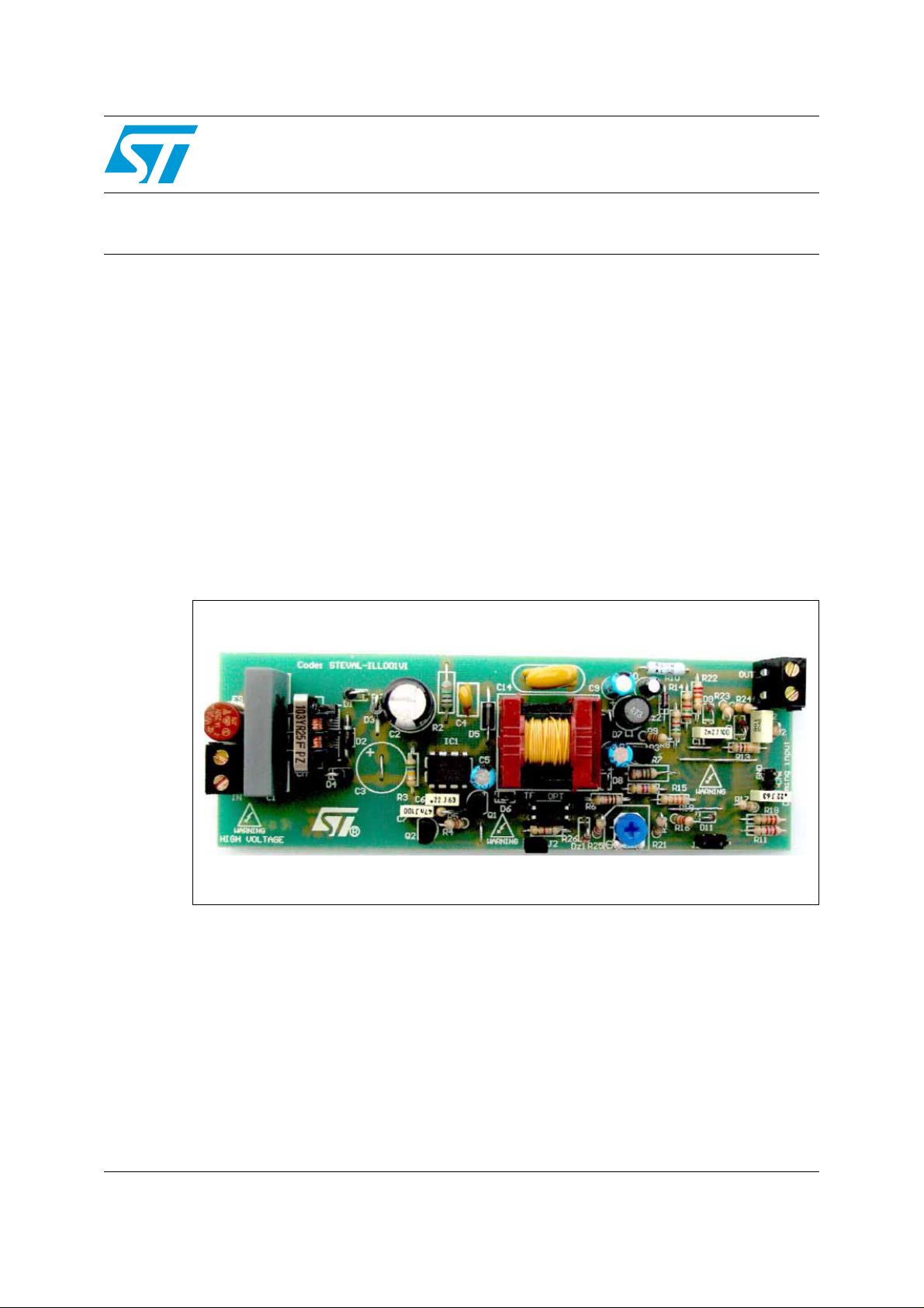
10W Dimmable LEDs driver board layout
March 2007 Rev 4 1/30
www.st.com
Page 2

Contents AN2042
Contents
1 Light sources . . . . . . . . . . . . . . . . . . . . . . . . . . . . . . . . . . . . . . . . . . . . . . . 4
2 Light emitting diode and colour vision . . . . . . . . . . . . . . . . . . . . . . . . . . 5
3 Commercial LEDs . . . . . . . . . . . . . . . . . . . . . . . . . . . . . . . . . . . . . . . . . . . 7
4 New dimming technique . . . . . . . . . . . . . . . . . . . . . . . . . . . . . . . . . . . . . . 8
5 Application description . . . . . . . . . . . . . . . . . . . . . . . . . . . . . . . . . . . . . 11
5.1 Dimming control circuit . . . . . . . . . . . . . . . . . . . . . . . . . . . . . . . . . . . . . . . 12
5.2 Transformer specifications . . . . . . . . . . . . . . . . . . . . . . . . . . . . . . . . . . . . 16
5.3 DALI Interface . . . . . . . . . . . . . . . . . . . . . . . . . . . . . . . . . . . . . . . . . . . . . . 16
6 Experimental results . . . . . . . . . . . . . . . . . . . . . . . . . . . . . . . . . . . . . . . . 18
7 Layout considerations . . . . . . . . . . . . . . . . . . . . . . . . . . . . . . . . . . . . . . 23
8 EMI measurements . . . . . . . . . . . . . . . . . . . . . . . . . . . . . . . . . . . . . . . . . 24
9 Non dimmable version . . . . . . . . . . . . . . . . . . . . . . . . . . . . . . . . . . . . . . 25
10 Input section arrangement for U.S. market . . . . . . . . . . . . . . . . . . . . . . 26
11 Conclusions . . . . . . . . . . . . . . . . . . . . . . . . . . . . . . . . . . . . . . . . . . . . . . . 27
12 Revision history . . . . . . . . . . . . . . . . . . . . . . . . . . . . . . . . . . . . . . . . . . . 29
2/30
Page 3

AN2042 List of figures
List of figures
Figure 1. Light emitting diode structure . . . . . . . . . . . . . . . . . . . . . . . . . . . . . . . . . . . . . . . . . . . . . . . . 5
Figure 2. The electromagnetic spectrum and visible region of light. . . . . . . . . . . . . . . . . . . . . . . . . . . 6
Figure 3. Human relative vision curve . . . . . . . . . . . . . . . . . . . . . . . . . . . . . . . . . . . . . . . . . . . . . . . . . 6
Figure 4. C.I.E. chromaticity diagram. . . . . . . . . . . . . . . . . . . . . . . . . . . . . . . . . . . . . . . . . . . . . . . . . . 7
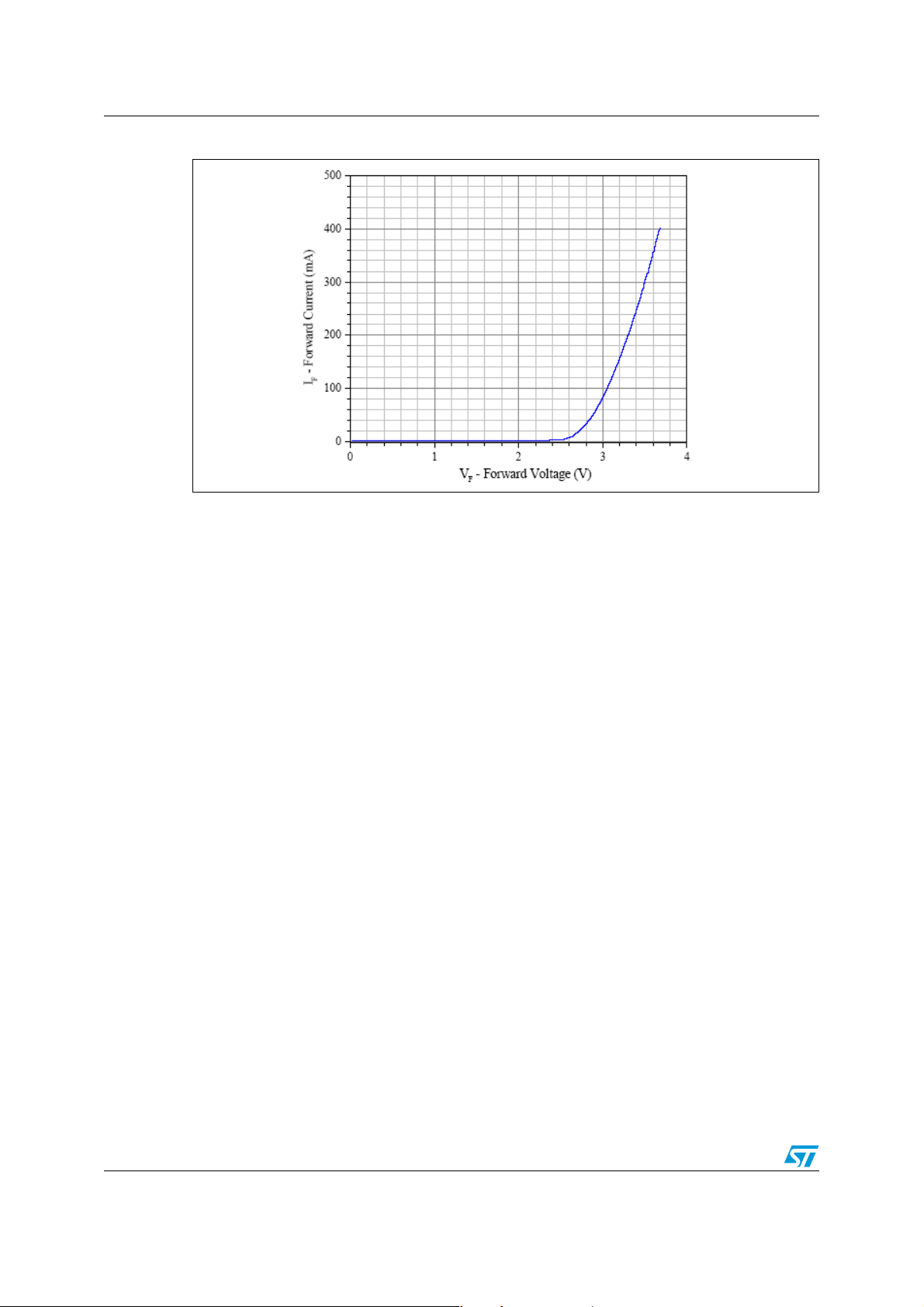
Figure 5. Forward current vs. forward voltage in a typical commercial LEDs . . . . . . . . . . . . . . . . . . . 8
Figure 6. PWM technique for dimming. . . . . . . . . . . . . . . . . . . . . . . . . . . . . . . . . . . . . . . . . . . . . . . . . 9
Figure 7. Brightness variation versus duty cycle . . . . . . . . . . . . . . . . . . . . . . . . . . . . . . . . . . . . . . . . . 9
Figure 8. Dimming technique using series switch . . . . . . . . . . . . . . . . . . . . . . . . . . . . . . . . . . . . . . . 10
Figure 9. Dimming technique using the new methodology . . . . . . . . . . . . . . . . . . . . . . . . . . . . . . . . 10
Figure 10. New dimming technique: typical waveforms. . . . . . . . . . . . . . . . . . . . . . . . . . . . . . . . . . . . 11
Figure 11. Converter schematic for European input voltage range . . . . . . . . . . . . . . . . . . . . . . . . . . . 14
Figure 12. Transformer features: (a) schematic, (b) mechanical characteristics and (c) pinout . . . . . 17
Figure 13. V
Figure 14. V
Figure 15. Typical waveforms: drain voltage and outp ut curr e nt ripple at 23 0 V
Figure 16. Typical waveforms: startup at 265 V
Figure 17. Drain voltage V
Figure 18. Drain voltage V
Figure 19. Drain voltage V
Figure 20. Drain voltage V
Figure 21. Drain voltage V
Figure 22. Drain voltage V
Figure 23. Control signals at 230 V
Figure 24. Control signals at 230 V
Figure 25. Control stage at 230 V
Figure 26. Control stage at 230 V
Figure 27. Open load condition at 230 V
Figure 28. Open load condition at 230 V
Figure 29. Efficiency . . . . . . . . . . . . . . . . . . . . . . . . . . . . . . . . . . . . . . . . . . . . . . . . . . . . . . . . . . . . . . 22
Figure 30. PCB layout (not in scale) . . . . . . . . . . . . . . . . . . . . . . . . . . . . . . . . . . . . . . . . . . . . . . . . . . 23
Figure 31. Conducted emissions at full load: line 1 emissions . . . . . . . . . . . . . . . . . . . . . . . . . . . . . . 24
Figure 32. Conducted emissions at full load: line 2 emissions . . . . . . . . . . . . . . . . . . . . . . . . . . . . . . 24
Figure 33. Non dimmable solution . . . . . . . . . . . . . . . . . . . . . . . . . . . . . . . . . . . . . . . . . . . . . . . . . . . . 25
Figure 34. Application circuit for U.S. input volta ge range: changes on the input section. . . . . . . . . . 26
Figure 35. STEVAL-ILL001V1 Schematic . . . . . . . . . . . . . . . . . . . . . . . . . . . . . . . . . . . . . . . . . . . . . . 28
and ID at 230 VAC: 1 LED . . . . . . . . . . . . . . . . . . . . . . . . . . . . . . . . . . . . . . . . . . . . . . 18
DS
and ID at 230 VAC: 8 LEDs . . . . . . . . . . . . . . . . . . . . . . . . . . . . . . . . . . . . . . . . . . . . . 18
DS
and output current I
DS
and output current I
DS
and output current I
DS
and output current I
DS
and output current I
DS
and output current I
DS
: 1 LED . . . . . . . . . . . . . . . . . . . . . . . . . . . . . . . . . . . . . . . . . . . 21
AC
: 8 LEDs . . . . . . . . . . . . . . . . . . . . . . . . . . . . . . . . . . . . . . . . . . 21
AC
: 1 LED . . . . . . . . . . . . . . . . . . . . . . . . . . . . . . . . . . . . . . . . . . . . 21
AC
: 8 LEDs . . . . . . . . . . . . . . . . . . . . . . . . . . . . . . . . . . . . . . . . . . . 21
AC
AC
AC
. . . . . . . . . . . . . . . . . . . . . . . . . . . . . . . . . . . . . . . . 19
AC
: 1 LED. . . . . . . . . . . . . . . . . . . . . . . . . . . . . . . 19
OUT
: 8 LEDs . . . . . . . . . . . . . . . . . . . . . . . . . . . . . . 19
OUT
at 50% dimming: 1 LED . . . . . . . . . . . . . . . . . 20
OUT
at 50% dimming: 8 LEDs . . . . . . . . . . . . . . . . 20
OUT
at 10% dimming: 1 LED . . . . . . . . . . . . . . . . . 20
OUT
at 10% dimming: 8 LEDs . . . . . . . . . . . . . . . . 20
OUT
: no dimming. . . . . . . . . . . . . . . . . . . . . . . . . . . . . . . . . . . 22
: minimum dimming . . . . . . . . . . . . . . . . . . . . . . . . . . . . . 22
. . . . . . . . . . . . . . . 19
AC
3/30
Page 4

Light sources AN2042
1 Light sources
Incandescent lights are basically electric space heaters that give off light as a by-product.
They are very inefficient, wasting most of the power they cons ume as heat.
An innovative light source is represented by LED technology, with very low power
consumption and virtually no heating effect, making LEDs ideal for several domestic and
commercial applications.
The long lifetime characteristic of LEDs means savings on maintenance costs. Unlike
traditional light sources, LEDs are not subject to sudden f ailure or b urnout. Since LED based
light sources last at least 10 times longer than a normal light source (up to 10 years or
100.000 hours for the higher quality products), it is possible to reduce or eliminate the
maintenance ongoing costs.
This can be useful in many critical applications where the location makes replacement
difficult (radio tower, aircraft warning lights, bridge and tunnel lights…) or in applications
where a failure of the light source is not acceptable (emergency exit lights, back up lighting,
security lighting…).
LED lighting technology features many advantages compared to conventional lighting:
● Higher energy efficiency, in terms of lumens per watt;
● Direct light beam for increasing system performance;
● Dynamic color control technology;
● Full dimmable without color variation;
● No mercury and no UV or heat in light beam;
● Low voltage operation, suitable fo r safety purpose in SELV systems.
The most important limitation for using high brightness LEDs is the manufacturing cost,
which is still relatively high.
In Table 1 a comparison between traditional light sources and a typical commercial LED is
shown.
Table 1. Performance of typical light sources compared with whi te Luxeon LEDs
Lighting source
Incandescent bulbs 18 ÷ 25 1000 – 2000 15 – 1000 W
Halogen lamps 15 – 25 2000 – 5000 5 – 2000 W
Fluorescent lamps 60 – 110 14000 – 20000 4 – 60 W
Mercury lamps 15 – 60 12000 – 24000 50 – 1000 W
LEDs (white luxeon) 25 100000 0.7 – 5 W
Luminous efficiency
(lm/W)
Lifetime (hours)
Theoretical optical
power (min and max)
4/30
Page 5
AN2042 Light emitting diode and colour vision
2 Light emitting diode and colour vision
Light-emitting diodes (LEDs) used for illumination are solid-state devices that produce light
by passing electric current across layers of semiconductor chips that are housed in a
reflector , which in tu rn is encased in an epoxy lens. The semiconductor material determines
the wavelength and subsequent color of the light. The lens converts the LED into a
multidirectional or unidirectional light source based on specification.
The first generation of LED was based on Gallium Arsenide (GaAs), Gallium Arsenide
Phosphide (GaAsP), Gallium Phosphide (GaP) technology, but thanks to the growth of solid
state technology, new structures have been introduced based on Aluminum Indium Gallium
Phosphide (AlInGaP), Indium Gallium Nitride (InGaN) or Gallium Aluminum Arsenide
(AlGaAs), mainly for the high brightness LEDs branch.
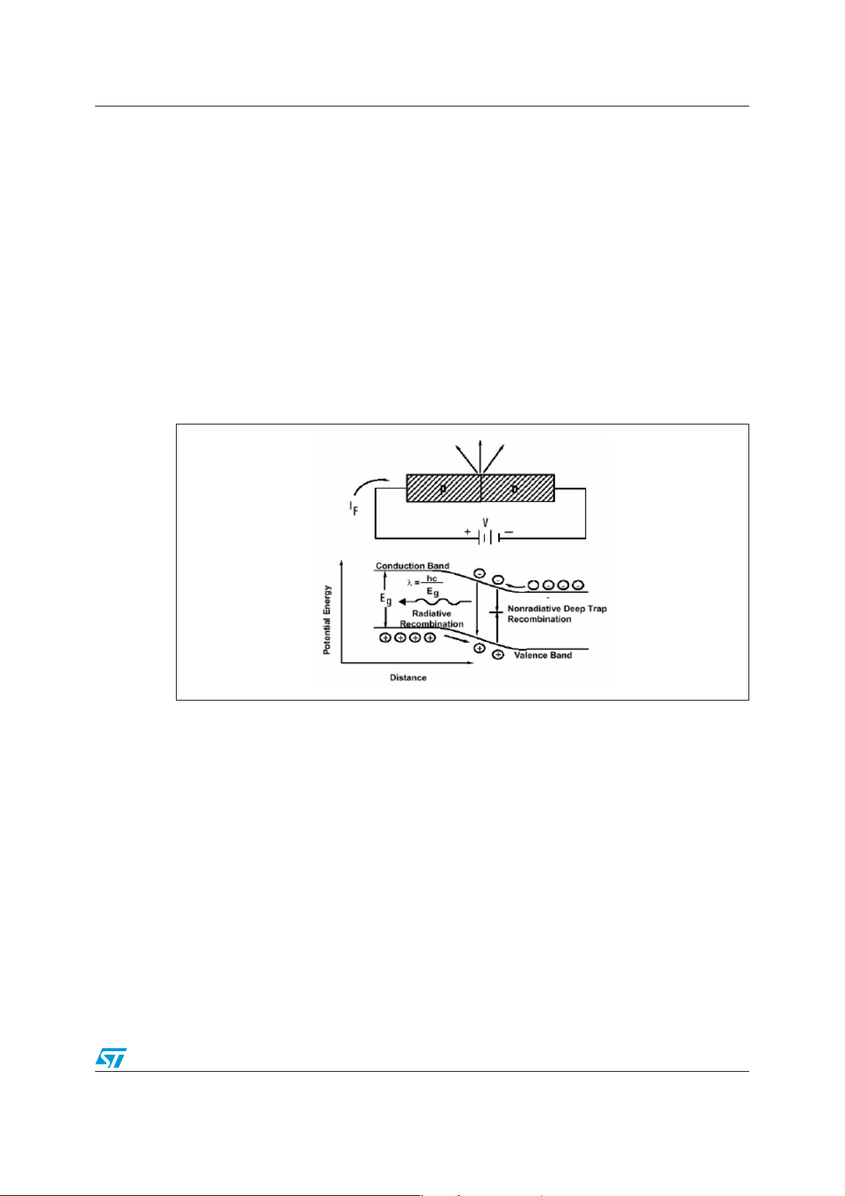
In Figure 1 the basic LED structure and the energy bands are shown.
Figure 1. Light emitting diode structure
The junction in an LED is forward biased and when electrons cross the junction from the n to
the p type material, the electron-hole recombination results in a process called
electroluminescence: when the applied voltage driv es the electrons and holes into the activ e
region between the n-type and p-typ e material, the ene rgy can be converted into infrared or
visible photons. This implies that the electron-hole pair drops into a stabler bound state,
releasing energy on the order of elect ron volts by emission of a photon of energy, according
to (Equation 1).
Equation 1
h
c
Egh
-----=•=
υ
c
λ
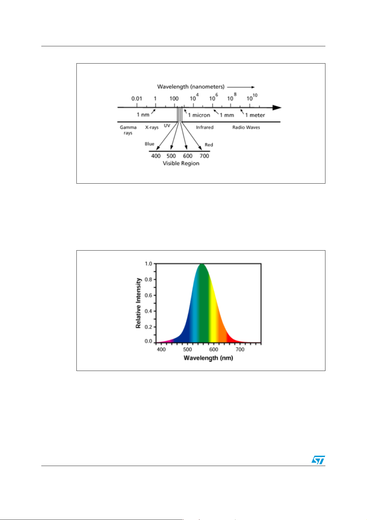
The human eye is excited in response to electromagnetic radiat ions with wavelengths in a
tight range of the electromagnetic spectrum, as shown in Figure 2, from 400 nm to 700 nm
which corresponds to extreme red and violet respectively.
5/30
Page 6
Light emitting diode and colour vision AN2042
Figure 2. The electromagneti c spectrum and visible region of light
The red extreme of the visible spectrum, 700 nm, requires an energy release of 1.77 eV to
provide the quantum energ y of the phot on. At the other e xtreme , 400 nm in the violet, 3. 1 eV
is required.
The human vision efficacy is not constant in the entir e visible region, b ut decreases near the
edges, as shown in Figure 3 featuring a peak value for a wavelength of 555 nm (greenyellow).
Figure 3. Human relative vision curve
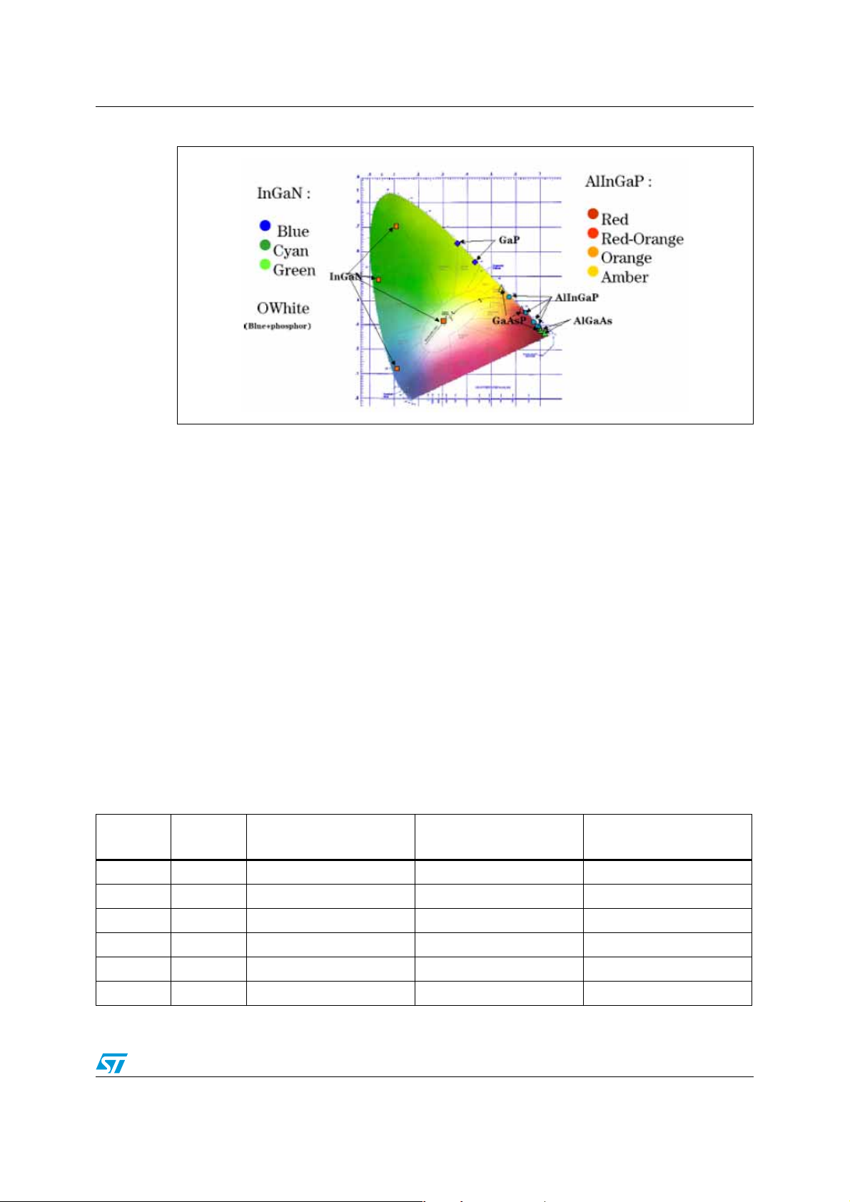
Wavelength can be defined in terms of dominant wavelength and x-y chromaticity
coordinates, which define the color as perceived by the human eye. The dominant
wavelength is derived from the C.I.E.
(Commission Internationale de l'Eclairage - International Commission on Illumination)
Chromaticity Diagram, as shown in Figure 4 This is an international standard for primary
colors established in 1931. Based on the f act that the human e y e is able to separat ely sense
three different portions of the spectrum (we identify these peak sensitivities as red, green
and blue), the eyes response is best described in terms of such primary colors. All the other
colors are defined as weighted sum of them.
6/30
Page 7
AN2042 Commercial LEDs
Figure 4. C.I.E. chromaticity diagram
3 Commercial LEDs
In the last years, light emitting diodes can be chosen from a wide variety of products
designed to meet specific needs to provide more efficient, longer life time alternatives to
traditional incandescent lamps.
They are manufactured of GaN and related compounds of AlGaN and InGaN due to the
wide bandgap, which allows emission of light ranging from the red to the ultraviolet (UV)
wavele ngth. Blue an d green LEDs are of special int erest and are be ing used in a wide range
of applications from outdoor video displays to automotive and cell phone backlights. LEDs
for solid-state white lighting offer high efficiency, long lifetime and a high degree of design
flexibility for a variety of lighting applications.
Thanks to new solid state technology, it now delivers from 25 to more then 120 lm/W in white
and comparable light output in other colors. In Table 2 are listed the main specifications for
typical commercial high efficiency LEDs are listed, while Figure 5 shows a typical V-I
characteristic for a high efficiency LED.
Table 2. Typi cal characteristic for commercial LEDs (from Luxeon)
Color
White 3.42 350 5500 K 18
Blue 3.42 350 470 nm 5
Cyan 3.42 350 505 nm 30
Green 3.42 350 530 nm 25
Amber 2.85 350 590 nm 20
Red 2.85 350 625 nm 25
Operating
voltage (V)
Operative forward current
(mA)
Dominant wavelength/
color temperature
Typical lu minous flux (lm)
7/30
Page 8
New dimming technique AN2042
Figure 5. Forward current vs. forward volta ge in a typical commercial LEDs
4 New dimming technique
Nowadays, thanks to the growth of process, packaging and therm al transfer technologies,
light output continues to evolve. This involves especially the InGaN technology, which
produces light output across blue, cyan, green and white, with high reliability and efficiency.
The wavelength of the light emitted is strongly dependent on the forward current driven
through the device and in order to avoid shifts in color the dimming strategies have to be
chosen carefully.
The most common method of dimming a LED is by varying either f o rw ard current or voltage
across it. Unfortunately, due to the characteristics of InGaN, varying current or voltage will
shift the wavelength. This effect is proportional to the wavelength, with the longer
wavelengths undergoing the strongest shift variation versus current.
In many applications this effect cannot be accepted and, employ ing a PWM technique, it is
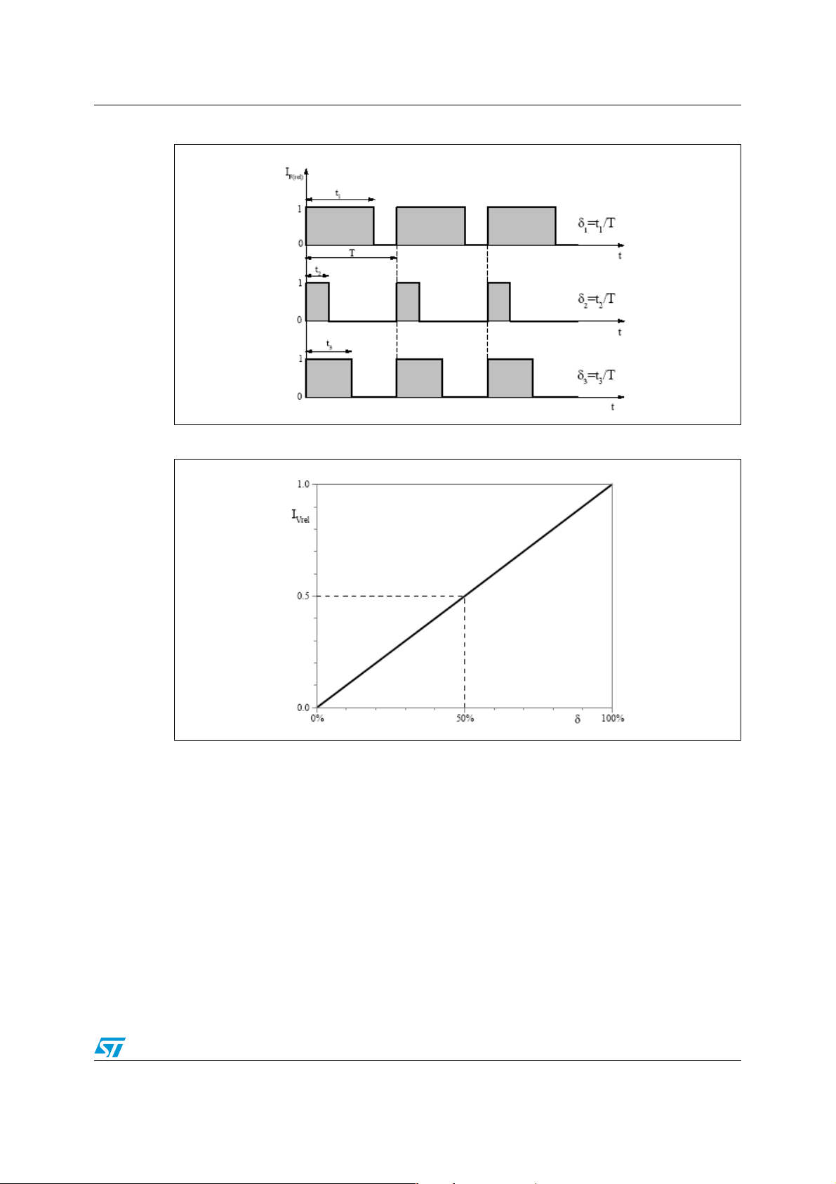
possible to dim a LED in the right manner, without wavelength shift.
The LED is switched on and off at constant f orward current (I
shown in Figure 6.
If the PWM frequency is higher than 100 Hz, the human eyes cannot perceive the single
pulses, but they integrate and interpret those pulses as brightness, which can be changed
linearly by varying the duty cycle linearly, with no wavelength shift. Figure 7 shows the
brightness variation versus duty cycle.
) by varying the duty cycle, as
F
8/30
Page 9
AN2042 New dimming technique
Figure 6. PWM technique for dimming
Figure 7. Brightness variation versus duty cycle
As shown in Figure 8, the most common method to dim LEDs consists in a series
connection of a power switch which is controlled by PWM.
Due to the relatively high operative forward current, the switch has to be selected carefully in
order to handle the conduction losses.
9/30
Page 10

New dimming technique AN2042
Figure 8. Dimming technique using series switch
To overcome this problem, a patented solution has been implemented, which allows to
eliminate the series switch, with a considerable improvement in terms of efficiency.
The new technique consists in a double control loop: a current and a voltage control loops.
The first one drives the LEDs with constant current when the maximum luminosity is
required. During the dimming operation, the current control loop will still limit the maximum
output current, while the voltage loop will maintain the output voltage below the threshold
voltage of the LEDs arra y. Also disconnecting the LEDs, the maximum output voltage will be
limited by the voltage loop. In Figure 9 and Figure 10 the block diagram of the new dimming
technique and the temporal diagrams are respectively shown. Thanks to t he absence of the
power swit ch, it is possible to have a more efficient and cheaper solution.
Figure 9. Dimming technique using the new methodology
10/30
Page 11

AN2042 Application description
Figure 10. New dimming technique: typical waveforms
5 Application description
The proposed converter is based on VIPer22A-E, a smart power with a current mode PWM
controller, startup circuit and protections integrated in the same monolithic chip, using
STMicroelectronics VIPower M0 Technology. The power stage consists in a vertical Power
MOSFET with 730 V breakdown voltag e and 0.7 A typical peak drain current.
The application consists in an isolated constant current pow er supply, intended to supply an
array of eight high efficiency LEDs, as shown in Figure 11.
The board has been designed referenced to the specifications listed in Table 3 It is
important to highlight that the converter works in single range, but both U.S. and European
range can be selected, with only a few modifications in the input section.
Table 3. SMPS Specifications
Parameters Value
Selectable Input voltage range 85V
Nominal output voltage range 3.5 V÷28 V
Maximum output voltage at open load 32 V
Output current 350 mA
Dimming range 0%÷90%
÷135 VAC or 185 VAC÷265 VAC
AC
EMI Standard EN55015:2000
11/30
Page 12

Application description AN2042
In the input stage, an EMI filter is implemented (C1, CM, C2) for both differential and
common mode noise, in order to fit the EN55015:2000 standard (limits for electrical lighting
and similar equipment). The input resistor R
, limits the inrush current of the capacitors at
1
plug-in and a standard fuse is also introduced to prevent catastrophic failure.
The clamping network (R
2-C4-D5
), limits the peak of the leakage inductance voltage spike,
assuring reliable operation of the VIPer22A-E.
The auxiliary winding on the primary side, is connected in forward mode, since the output
voltage ranges from 3.5 V to 28 V and the voltage on VDD pin varies from 17 V to 24 V.
A brown-out circuit (R
, R4, R5, Q1, Q2 and C7) is implemented in order to avoid the
3
flickering of the LEDs during switch off. The values of R
get the given thresholds, while C
stabilizes the voltage on the base of Q1.
7
The output filter selection is a very critical point to consider during the design. Since LEDs
are switched on and off during the dimming phase the value of the output capacitor has to
be as low as possible.
Therefore , in order to a void exce eding the maximum ou tput current ripple , care must be paid
to design the right LC post filter.
5.1 Dimming control circuit
The current loop is controlled by the second operational amplifier of TSM104W and the
sense resistor R
R
and R14) connected to the 2.5 V internal voltage reference V
13
bridge should be 1% precision in order to get the best precision on the regulation. The
current control equations are given by (Equation 2) and (Equation 3).
Equation 2
. The voltage threshold is generated by means of a resistor bridge (R12,
10
V
Iout()
V
•
REFR14
----------------------------------------- -=
++
R
12R13R14
, R4 and R5 are chosen in order to
3
. The resistors of the
REF
Equation 3
I
OUT
The sense resistor R
, is chosen taking into account the maximum dissipation during full
10
load. The voltage loop is controlled by the third operational amplifier and the v olt ag e divider
R
and R9 directly connected to the output. Th e values are chosen according the equations
8
(Equation 4) and (Equation 5).
Equation 4
V
Oref
Equation 5
V
Oref
Where V
OUT(MAX)
disconnected. The transistor Q
is the maximum acceptable output voltage, when the LEDs array is
, connected to the dimming control section, is ON during
3
normal operation.
12/30
V
•=
Iout()R10
V
REFR13R14
-------------------------------------------------- -=
R
12R13R14
V
-----------------------------=
+()•
++
OUT MA X()
R8R9+
Page 13

AN2042 Application description
The feedback to the primary side is achieved thanks to the diodes D9 and D10, which
decouple the two loops and drive the optocoupler OPT. The legs R
and R24-C12 are
23-C11
connected for feedback stabilization.
The zener diode D
is connected at the non-inverting input of the voltage control
Z2
operational amplifier in order to clamp the maximum voltage on the pin in any operative
condition.
The PWM control is realized using the first operational amplifier to generate a sawtooth
waveforms at 270 Hz (given by the leg R
(set by the potentiometer R
): the generated signal will drive the NPN transistor Q3. When
21
), which is compared with a variable voltage
19-C13
the transistor is "ON", the SMPS works in "current control" mode limiting the max output
current while, when the tr ansistor is "OFF", it works in "v olta ge control" m ode, regulatin g the
output voltage below the LEDs threshold and consequently switching them off.
During the dimming operation, the transistor Q
IC2 is pulled up and limited to V
. Consequently, the VIPer stops swit ching and the output
DZ1
current falls to zero, while the output voltage decrease down to V
is the number of LEDs and V
is the threshold voltage. Further decrease of the output
F(OFF)
is switched off and the voltage on pin 11 of
3
OUT
= n · V
F(OFF)
, where n
voltage is not possible because of the high output impedance. Doing so, the output voltage
never falls to zero, resulting in a big improvement in the dynamic behavior of the dimming
function, with a slight impact on the efficiency P
In open load condition, the maximum voltage is regulated by R
DISS
= (V
OUT-VDZ2
, R9 and DZ2 according to
8
)/R8.
the reference voltage given by (Equation 5).
13/30
Page 14

Application description AN2042
Figure 11. Converter schematic for European input voltage range
14/30
Page 15

AN2042 Application description
Table 4. Component list
Reference Description Note
FS 1 A-250 V Fuse
R1 10., 1/2 W
R2 1M., 1/2 W
R3 560 k., 1/4 W
R4 12 k., 1/4 W
R5 24 k., 1/4 W
R6 1 k., 1/4 W
R7 150., 1/2 W
R8 5.6 k., 1/4 W
R9 220., 1/4 W
R10 0.47., 1/4 W Sense resistor
R11 2.7 k., 1/4 W
Metallic oxide resistor – No
flammable
R12 12 k., 1/4 W
R13 10 k., 1/4 W
R14 1.5 k., 1/4 W
R15 4.7 k., 1/4 W
R16, R18, R22 22 k., 1/4 W
R17 100., 1/4 W
R19 33 k., 1/4 W
R20 15 k., 1/4 W
R21 20 k., 1/4 W Potent io me te r
R23, R24 220 k., 1/4 W
R25 1.2 k., 1/4 W
R26 6.8 k., 1/4 W
C1 100 nF, 275 V X2 Capacitor
C2 10 µF, 400 V Electrolytic capacitor
C4 100 pF, 630 V Polypropylene capacitor
C5 33 µF, 25 V Electrolytic capacitor
C6, C13 220 nF Polyester capacitor
C7 47 nF Polyester capacitor
C8 33 µF, 16 V Electrolytic capacitor
C9 1 µF, 50 V Electrolytic capacitor
C10 3.3 µF, 50 V Electrolytic capacitor
15/30
Page 16

Application description AN2042
Table 4. Component list (continued)
Reference Description Note
C11, C12 2.2 nF Polyester Capacitor
C14 2.2 nF, 250 V Y1 Capacitor
D1, D2, D3, D4 1N4007
D5 STMicroelectronics STTH1R06
D6, D8, D9, D10, D11 1N4148
D7 STMicroelectronics STTH102
DZ1, DZ2 Zener Diode 5.1 V, 1/4 W
Q1, Q3 STMicroelectronics BC337 NPN transistor
Q2 STMicroelectronics BC327 PNP transistor
L1 47 µH Radial
TF TDK SRW16ES-ExxH003
CM Coilcraft BU9-103R25B 2X10 mH Common mode choke
OPT SFH610A
IC1
STMicroelectronics
VIPer22ADIP-E
IC2 STMicroelectronics TSM104
5.2 Transformer specifications
The transformer has four windings, included two auxiliaries. One is used to supply the VIPer
and the other one to supply the TSM104 and the dimming control circuit on the secondary
side.
Since the output voltage is variable between 3.5 V (with 1 LED) and 28 V (with 8 LEDs) , the
two auxiliary windings are coupled in forward mode to the primary winding.
In order to limit the reflected voltage to a maximum v alue (100 V), t he primary-to-secondary
turn's ratio has been set according to the maximum count of LEDs.
The transformer characteristics are listed in Table 5 and the winding arrangement as well as
the mechanical specifications are shown in Figure 12
5.3 DALI Interface
In order to control the board in re mot e fashion a connector has been introduced to interface
it with the DALI reference design (ST7DALI-EVAL).
Referring to the schematic in Appendix A, it is possible to move from analog control by the
trimmer R
1..10 V output of the DALI interface on connector J2 of the ST7DALI-EVAL demo board to
CN1 connector of the STEVAL-ILL001V1, providing the correct voltage range, i.e. from 0 to
2.5 V.
to the digital one by DALI, removing the jumper J1 and J2. Then, connect the
21
16/30
Page 17

AN2042 Application description
Figure 12. Transformer features: (a) schematic, (b) mechanical characteristics and
(c) pinout
a
Table 5. Transformer specifications
Parameters Value
Ferrite PC40EF16
Core geometry E16
Primary inductance 2.0 mH±12%
Leakage inductance 60 µH max
NP 135 turns – AWG 35
NAUX1 9 turns – AWG 35
NAUX2 5 turns – AWG 29
NSEC 36 turns – AWG 29
b
c
17/30
Page 18

Experimental results AN2042
6 Experimental results
In this section typical waveforms are given under several load conditions. In Figure 13 and
Figure 14 the drain-source voltage and the drain current at mini mum load (1 LEDs) and full
load (8 LEDs), at nominal input voltage (230 V
output current ripple is shown, which is fix ed to about 20% IOUT, in order to keep the out put
filter small and improve the output dynamic behavior.
In Figure 17 to Figure 22 the output current and drain-source voltage are shown during
dimming operations. It is important to point out that the driver is able to dim the LEDs array
down to 10% of its maximum luminosity.
In Figure 23 and Figure 24 typical waveforms of the dimming control section, as introduced
in Section 5.1, are shown: the sawtooth w aveform, VSAW, defines the dimming frequency
while varying the reference voltage, V
, by means of the potentiometer R21, it is possible
REF
to change the PWM duty-cycle and consequently the LEDs luminosity. It is important to
point out that the output v oltage never goes to zero, but is always abo ve a minimum value
depending on the number of LEDs in the arr a y. In Figure 25 and Figure 26 the output during
dimming is shows.
Finally, Figure 27 and Figure 28 shows the drain voltage and output voltage in open load
condition with 1 or 8 LEDs connected respectiv ely. Under this condition the outpu t v oltage is
limited to about 33 V both in steady state and dimming operation.
) are shown, respectively. In Figure 15 the
AC
Figure 13. V
and ID at 230 VAC: 1 LED Figure 14. VDS and ID at 230 VAC: 8 LEDs
DS
Ch1 freq - 58.18 kHz (black)
Ch2 max - 196 mA (green)
Ch1 freq - 58.18 kHz (black)
Ch2 max - 196 mA (green)
18/30
Page 19

AN2042 Experimental results
Figure 15. Typical waveforms: drain voltage
and output current ripple at 230 V
AC
Ch1 freq - 548 V (black)
Ch2 max - 348 mA (red)
Ch3Pk-Pk - 68 mA (red)
Figure 17. Drain voltage VDS and output
current I
OUT
: 1 LED
Figure 16. Typical waveforms: startup at
265 V
AC
Ch1 max - 610 V (black)
Figure 18. Drain voltage V
current I
OUT
and output
DS
: 8 LEDs
Ch1 max - 418 V (black)
Ch2 max - 348 mA (green)
Ch1 max - 542 V (black)
Ch2 mean - 352.6 mA (green)
19/30
Page 20

Experimental results AN2042
Figure 19. Drain voltage VDS and output
current I
at 50% dimming: 1 LED
OUT
Ch2 mean - 170.6 mA (green)
Ch2 duty - 51.63% (green)
Ch2 freq - 246 Hz (green)
Figure 21. Drain voltage V
current I
OUT
and output
DS
at 10% dimming: 1 LED
Figure 20. Drain voltage V
current I
at 50% dimming: 8
OUT
LEDs
Ch2 mean - 171.1 mA (green)
Ch2 duty - 50.52% (green)
Ch2 freq - 245 Hz (green)
Figure 22. Drain voltage V
current I
at 10% dimming: 8
OUT
LEDs
and output
DS
and output
DS
Ch2 mean - 33.9 mA (green)
Ch2 duty - 10.18% (green)
Ch2 freq - 252 Hz (green)
20/30
Ch2 mean - 31.5 mA (green)
Ch2 duty - 8.8% (green)
Ch2 freq - 249 Hz (green)
Page 21

AN2042 Experimental results
Figure 23. Control signals at 230 VAC: 1 LED Figure 24. Control signals at 230 VAC: 8 LEDs
Ch2 mean - 33.9 mA (green)
Ch2 duty - 10.18% (green)
Ch2 freq - 252 Hz (green)
Figure 25. Control stage at 230 VAC: 1 LED Figure 26. Control stage at 230 VAC: 8 LEDs
Ch1 mean - 200 mA (black)
Ch2 max - 3.48 V (green)
Ch2 min - 2.44 V (green)
Ch2 mean - 31.5 mA (green)
Ch2 duty - 8.8% (green)
Ch2 freq - 249 Hz (green)
Ch2 mean - 197.4 mA (black)
Ch2 max - 26.6 V (green)
Ch2 min - 20.2 V (green)
21/30
Page 22

Experimental results AN2042
Figure 27. Open load condition at 230 V
dimming
AC
: no
Ch1 freq - 613 Hz (black)
Ch2 max - 32.8 V (green)
The efficiency of the system, one of the k ey parameters of the application, has been
measured in the whole input voltage range varying the number of LEDs from 1 to 8, and the
experimental results are shown in Figure 29.
Figure 28. Open load condition at 230 VAC:
minimum dimming
Ch1 freq - 250 Hz (black)
Ch2 max - 33.6 V (green)
Figure 29. Efficiency
22/30
Page 23

AN2042 Layout considerations
7 Layout considerations
As any switched mode po wer supp ly, for proper operations , basic rules hav e to be ta ken into
account in order to optimiz e the curren t path, especially in the routing of high current path . In
fact, since EMI issues are also related to layout, the current loop area has to be minimized.
In addition to this, in order to avoid any noise interference between the control section and
the power section, the control ground paths have to be kept separated from each other. All
the high current traces have to be as short and wide as possible, in order to minimize the
resistive and inductive effect.
A particular care has to be taken regarding the optimal routing of the input EMI filter path
and the correct placement of any single component.
A final consideration regards the thermal management: a copp er area has to be pro vided on
the VIPer drain, in order to reduce the thermal resistance R
device temperatu re rea sona bly low. All the aforementioned considerations have been t aken
into account in the lab prototype, as shown in Figure 30.
Figure 30. PCB layout (not in scale)
and consequently keep the
th
23/30
Page 24

EMI measurements AN2042
8 EMI measurements
Conducted EMI measurements have been performed according to EN55015:2000, the
specific European standard on electrical lighting and similar equipment, using a 50 LISN
and a spectrum analyzer with peak detector.
The results are shown in Figure 31 and Figure 32, for Line 1 and Line 2 respectively, under
full load condition at nominal input voltage, i.e. 230 V
the Quasi Peak limit alt hough the measurements have been performed using the Peak
detector, conforming the conducted EMI compliance of the system.
Figure 31. Conducted emissions at full load: line 1 emissions
. The emissions level are well below
AC
Figure 32. Conducted emissions at full load: line 2 emissions
24/30
Page 25

AN2042 Non dimmable version
9 Non dimmable version
A lower cost solution is introduced as shown in Figure 33, if the dimming function is not
required. In this case the TSM104 used for the dimming control is replaced by the simpler
TSM1011 and the brown-out circuit is not necessary anymore during the switch off of the
circuit. No other changes need to be introduced neither the transformer specifications nor
the voltage and current thresholds have to be changed.
The dimming control section is eliminated and the TSM104 is replaced by the simplest
TSM1011. Moreover, the brownout circuit is not necessary during the switch off. The same
rules to design to define the transformer specifications and voltage and current thresholds
are still valid.
Figure 33. Non dimmable solution
25/30
Page 26
Input section arrangement for U.S. market AN2042
10 Input section arrangement for U.S. market
The proposed system has been designed for the European voltage range, i.e . 18 7-264 VAC,
but by means of a voltage doubler, consisting of D
the U.S . voltage range, i.e. 88-132 V
capacitor C
which has to be replaced b y two cap acitors C2 and C3 with half the value of the
2
. The only modification needed is related to the input
AC
European voltage range, connected as shown in Figure 34.
Figure 34. Application circuit for U.S. input voltage range: changes on the input
section
and C2-C3, it can also be used with
1-D2
26/30
Page 27

AN2042 Conclusions
11 Conclusions
In this document an innov ativ e solution for driving high efficiency LEDs has been introduced.
The power converter is based on a flyback topology with the sma rt power VIPer22A-E. It is
able to drive with no circuital modifications 1 to 8 LEDs array and to perform an optimal
dimming function by means of a patent ed PWM technique. A simplified version of the
system has also been introduced in order to address the low end applications which do not
require the dimming function.
A lab prototype has been developed and fully tested under several conditions, confirming
the suitability of the proposed approach to such an emerging application.
The reference board will be available at stock through the order code: STEVAL-ILL001V1.
27/30
Page 28
STEVAL-ILL001V1 schematic AN2042
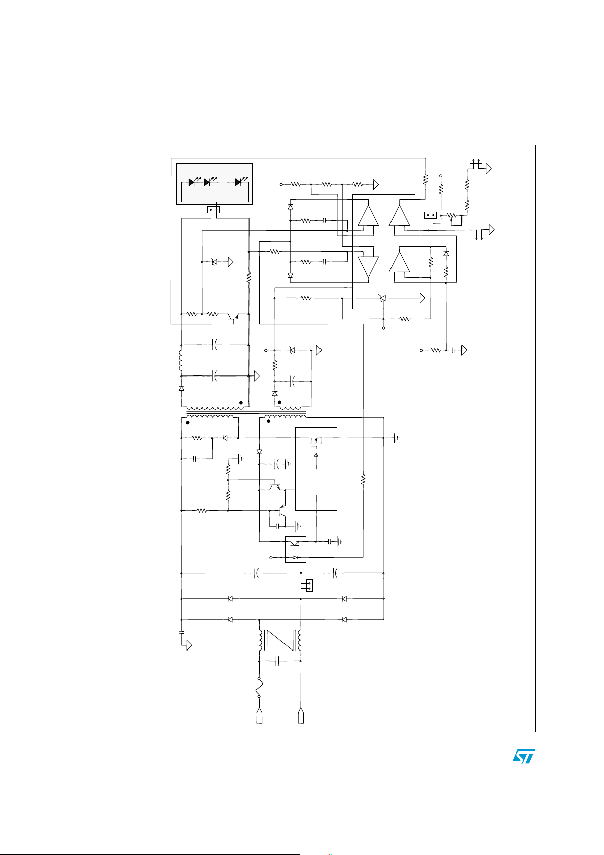
Appendix A STEVAL-ILL001V1 schematic
Figure 35. STEVAL-ILL001V1 Schematic
J2
LD1
LD2
OUT
LD8
R12
Vref
D10
R13
R24
C12
R14
10
3
--+
111256749
4
-
+
+Vcc
R15
R20
J1
R26
R25
R21
DZ2
R10
R9
R8
L1
D7
R2
C4
R3
Q3
C10
+
C9
+
D5
R5
R4
D3
R22
R23
D9
DZ1
+Vcc
R7
C8
+
D8
D6
C5
+
Q1
Q2
C7
OPT
+Vcc
+
C2
C11
R11
DRAIN
VDD
SOURCE
IC1
CONTROL
FB
C6
+
C3
J3
D4
IC2
-
+
2
R6
1
-
+
8
R18
Vref
D11
R16
R17
13 2 3 1 15 14 16
R19
+Vcc
CN1
C13
D1
C14
CM
C1
Fs
IN
IN
28/30
D2
Page 29

AN2042 Revision history
12 Revision history
Table 6. Revision history
Date Revision Changes
Oct-2004 1 First issue
Feb-2005 2 D5 & Q2 values change in component list table
Feb-2005 3
21-Mar-2007 4
– Figure in cover page changed
– Bil of material modified
– The document has been reformatted
– Figure in cover page changed
– PCB layout changed
– STEVAL-ILL001V1 Schematic insertion
29/30
Page 30

AN2042
Please Read Carefully:
Information in this document is provided solely in connection with ST products. STMicroelectronics NV and its subsidiaries (“ST”) reserve the
right to make changes, corrections, modifications or improvements, to this document, and the products and services described herein at any
time, without notice.
All ST products are sold pursuant to ST’s terms and conditions of sale.
Purchasers are solely res ponsibl e fo r the c hoic e, se lecti on an d use o f the S T prod ucts and s ervi ces d escr ibed he rein , and ST as sumes no
liability whatsoever relati ng to the choice, selection or use of the ST products and services described herein.
No license, express or implied, by estoppel or otherwise, to any intellectual property rights is granted under this document. If any part of this
document refers to any third pa rty p ro duc ts or se rv ices it sh all n ot be deem ed a lice ns e gr ant by ST fo r t he use of su ch thi r d party products
or services, or any intellectua l property c ontained the rein or consi dered as a warr anty coverin g the use in any manner whats oever of suc h
third party products or servi ces or any intellectual property contained therein.
UNLESS OTHERWISE SET FORTH IN ST’S TERMS AND CONDITIONS OF SALE ST DISCLAIMS ANY EXPRESS OR IMPLIED
WARRANTY WITH RESPECT TO THE USE AND/OR SALE OF ST PRODUCTS INCLUDING WITHOUT LIMITATION IMPLIED
WARRANTIES OF MERCHANTABILITY, FITNESS FOR A PARTICUL AR PURPOS E (AND THEIR EQUIVALE NTS UNDER THE LAWS
OF ANY JURISDICTION), OR INFRINGEMENT OF ANY PATENT, COPYRIGHT OR OTHER INTELLECTUAL PROPERTY RIGHT.
UNLESS EXPRESSLY APPROVED IN WRITING BY AN AUTHORIZED ST REPRESENTATIVE, ST PRODUCTS ARE NOT
RECOMMENDED, AUTHORIZED OR WARRANTED FOR USE IN MILITARY, AIR CRAFT, SPACE, LIFE SAVING, OR LIFE SUSTAINING
APPLICATIONS, NOR IN PRODUCTS OR SYSTEMS WHERE FAILURE OR MALFUNCTION MAY RESULT IN PERSONAL INJ URY,
DEATH, OR SEVERE PROPERTY OR ENVIRONMENTAL DAMAGE. ST PRODUCTS WHICH ARE NOT SPECIFIED AS "AUTOMOTIVE
GRADE" MAY ONLY BE USED IN AUTOMOTIVE APPLICATIONS AT USER’S OWN RISK.
Resale of ST products with provisions different from the statements and/or technical features set forth in this document shall immediately void
any warranty granted by ST fo r the ST pro duct or serv ice describe d herein and shall not cr eate or exten d in any manne r whatsoever , any
liability of ST.
ST and the ST logo are trademarks or registered trademarks of ST in various countries.
Information in this document su persedes and replaces all information previously supplied.
The ST logo is a registered trademark of STMicroelectronics. All other names are the property of their respective owners.
© 2007 STMicroelectronics - All rights reserved
STMicroelectronics group of compan ie s
Australia - Belgium - Brazil - Canada - China - Czech Republic - Finland - France - Germany - Hong Kong - India - Israel - Italy - Japan -
Malaysia - Malta - Morocco - Singapore - Spain - Sweden - Switzerland - United Kingdom - United States of America
www.st.com
30/30
 Loading...