

Page 1
AN2036
APPLICATION NOTE
Solderability Tests
Lead-free devices, fr om STMic roelectro nics, are warranted t o pass th e solderab ility te sts, and to form a
reliable solder joi nt with th e b as e m ateri al of the ci r cuit boa rd , u sing Lea ded (Sn-Pb) solder or Lea d-fr ee
(Sn-Ag-Cu) solder. This document describes the context of this assertion.
®
ST Lead-free devices confo rm t o the EC OPA CK
with the European directive on Restrictions on Hazardous Substances (RoHS) 2002/95/EU, and with the
IPC/JEDEC 020 standard for resistance to soldering heat and soldering process.
These devices have to be solderable with both Leaded materials and processes, and with Lead-free materials and processes. With a composition close to the ternary eutectic composition (Table 1.), the Tin-
Silver-Copper (Sn-Ag-Cu) alloy is considered as the standard lead-free material. Only Tin-Bismuth coated
devices are not te sted i n Tin- Lead solde r. Thi s is b ecaus e the Tin-B ismuth c oatin g is not r ecomm ended
for mixing with Tin-Lead solder, for board mounting, due to a reliability risk on the solder joints.
Table 1. Solder Composition for Solderability Tests
Solder Composition Range (% weight)
Lead-free
SnPb
7191395 specification from ST . This , in tur n, co mpl ie s
Tin 94.6 to 96.6
Silver 3.0 to 4.3
Copper 0.4 to 1.1
Tin 60 to 64
Lead 36 to 40
There are two kinds of tests that are applied to evaluate such ability of a surface to be wetted:
■ Dip and Look
■ Wetting Balance
Both tests are well kn own, and applie d, worldwide. H owever, d ifferent metho ds are often us ed (such a s
MIL standard 883-2003, JEDEC J-S TD- 002 , JESD2 2- B10 2 and IEC 60749- 21 ). The on es chosen by ST
are intended to cover the ones that are in most widespread use by our customers.
In these tests, the packages are “aged”, in order to test the solderability under the worst conditions and to
warrant at least 2 years of storage with no significant degradation of solderability.
1/7November 2004
Page 2
AN2036 - APPLICATION NOTE
DIP AND LOOK TEST
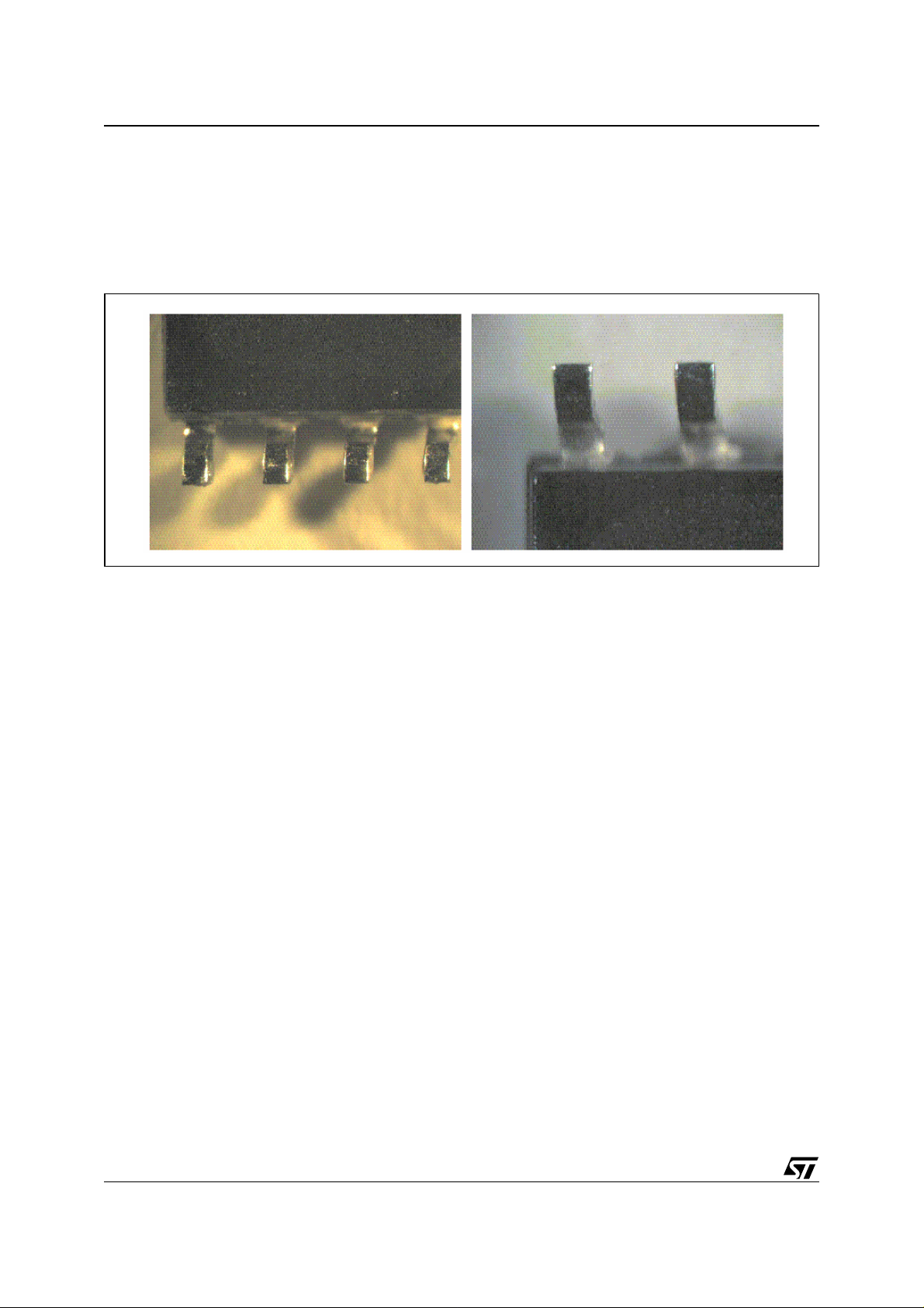
After appropriate ageing, the connections are dipped inside a non-activated flux, then into molten solder.
Then, after cooling and o ptional cleanin g in alcohol, the c onnections are ins pected to verify the critical
area (the one that is to be soldered to the board) of the connection surfaces is covered by fresh solder
(Figure 1.). The test is considered passed if 95% of the surface is covered with fresh solder.
Figure 1. Terminals after Dip and Look Test
The mechanism for forming the solder joint depends on the coating and solder compositions as well as on
the test conditions (as listed in Table 2.).
2/7
Page 3

AN2036 - APPLICATION NOTE
Table 2. Test Conditions
– 8 hours steam ageing or ageing in humidity chamber at 85°C and 85%rH (Humidity
chamber used for pre-plated components)
– Dry ageing at 150°C: 8 hours for NiPdAu Pre-plated units and 16 hours for solder coated
units (Ageing is non cumulative = to be done on different samples)
Sn-Ag-Cu melted at 245°C
Flux dipping 5 to 10 seconds
Lead-free
Solder
Solder dipping
Surface Mount
Devices
Leaded Solder
Solder Wave Resistance to Dissolution
8 hours steam ageing or ageing in humidity chamber at 85°C and 85%rH
Insertion Packages or
Through Hole
Devices
Note: Non activated flux to be 25% by weight of colophany diluted in isopropanol as per IPC J- STD004.
Lead-free Solder
Leaded Solder
Sn-Pb melted at 220°C
Flux dipping 5 to 10 seconds
Solder dipping
Device that can be soldered by wave soldering
Sn-Pb or Sn-Ag-Cu melted at 260°C
Flux dipping 5 to 10 seconds
Solder dipping 10 seconds ±0.5s
Sn-Ag-Cu melted at 245°C
Flux dipping 5 to 10 seconds
Solder dipping 5 seconds ±1s
Sn-Pb melted at 245°C
Flux dipping 5 to 10 seconds
Solder dipping 5 seconds ±1s
5 seconds ±0.5s for Tin
based connection coatings
10 seconds ±0.5 s for Preplated NiPd(Au) connections
5 seconds ±0.5s for Tin
based connection coatings
10 seconds ±0.5s for Preplated NiPd(Au) connections
3/7
Page 4

AN2036 - APPLICATION NOTE
WETTING BALANCE TEST
Connections are dipped insi de a non-activated flux. Th en the package is loaded on the wetti ng balance
arm, and the connections are dipped into a molten solder. The force exerted on the balance arm is plotted
as a function of time.
This test cannot be applied for all the packages. It can, though, be adjusted to fit special cases.
Typical forces versus time curves are shown in Figure 2.
Figure 2. Wetting Force Plotted against Time, for Three Cases
No Forced Ageing
Ageing:
16 hours, 150°C
Wetting force mN/mm
The shape of the curves can be explained as follows:
– At the beginning, the buoyancy forces (due to the interfacial tension) are predominant, and so the
wetting force is negative.
– Gradually, the solder begins to wet the terminals, and the wetting force increases with time,
overcoming the buoyancy force.
– Eventually, it reaches a flat (plateau) zone.
Ageing:
8 hours, 85°C and
85% Humidity
Immersion: 10 seconds
4/7
Page 5

AN2036 - APPLICATION NOTE
When the measured wetting force is zero, the two forces are balanced. This point is called the “zero cross
time” (t
greater than zero).
Note: No aging is appl ied , be for e th e wet tin g ba lan ce tes t, d ur ing pr oc es s con t rol of pr od uc tio n. A gi ng is
applied for data collection purpose only.
Criteria: the test is considered as passed if:
– The wetting force reaches 0.1mN/mm within 5 seconds of immersion
– The zero cross time (t0) is less than 3 seconds.
Note: these criteria are applied for small-signal devices. Power devices can require different criteria to take
into account the thermal mass of their connections.
Table 3. Tests Conditions
), and indicates the transition from no-wetting (overall force less than zero) to wetting (overall force
0
Solder
Sn-Ag-Cu melted at 245°C (±5°C)
Sn-Pb melted at 235°C (±5°C)
Flux dipping 5 to 10 seconds
Solder dipping 10 seconds
Flux dipping 5 to 10 seconds
Solder dipping 10 seconds
Note:
– The wetting force, as measured by the balance, is divided by the total perimeter of the connections at
initial immersion.
– In the case of leads that are connected to a thermal mass, such as to a dissipater, the test must be
redefined to include preheating.
CONCLUSIONS
Through two standard tests (“Dip and Look” and “Wetting Balance”), ST Lead-free devices are warranted
to pass solderability tests using Sn-Pb solder or Sn-Ag-Cu solder, and so to meet all the requirements for
electronics soldering. In fact the solderability tests provide customers with an additional warranty that the
components can be soldered without affecting the common reliability performance.
5/7
Page 6

AN2036 - APPLICATION NOTE
REVISION HISTORY
Table 4. Document Revision History
Date Version Revision Details
08-Nov-2004 1.0 First Issue
6/7
Page 7

AN2036 - APPLICATION NOTE
Information furnished is be lieved to be a ccur ate and reli able. Howe ver, STMicroele ctronic s assu mes no r esponsib ilit y for th e consequences
of use of such information nor for any infrin gement of patent s or other rights of third parties which ma y result from it s use. No license is granted
by implication or otherwi se under any patent or patent rights of STMicroelectronics. Specifications mentioned in this publication are subject
to change without not ice. This pub licat ion su persed es and repl aces all in format ion previou sly su pplie d. STMicroele c tronic s prod ucts ar e no t
authorized for use as critical compone nts in life support devices or systems without express written approval of STMicroelectronics.
The ST logo is a registered trademark of STMicroelectronics.
All other names are the property of their respective owners
© 2004 STMicroelectronics - All rights reserved
Australia - Belgium - Brazil - Canada - China - Czech Republic - Finland - France - Germany - Hong Kong - India - Israel - Italy - Japan -
Malaysia - Malta - Morocco - Singapore - Spain - Sweden - Switzerland - United Kingdom - United States of America
STMicroelectronics group of companies
www.st.com
7/7
 Loading...