

Page 1

AN2034
APPLICATION NOTE
Soldering Compatibility (Backward and Forward)
COMPATIBILITY OF LEAD-FREE COMPONENTS
The semiconductor industry is moving towards the elimination of lead from packages, in accordance with
new international regulations.
This concerns both solder paste , for the board mounting process, as well as semi-conductor package s
themselves.
A major impact is on the solder reflow process step, as most of the lead-free alloys under investigation for
solder paste melt at temperatures that are 30 to 40°C higher than eutectic SnPb (Tin, Lead) solder.
For a transitional period, leaded and lead-free technologies already coexist, either by having leaded packages mounted with lead-free paste or by having eutectic Sn/Pb paste used with lead-free components.
The tight collaboration be tween STM icroel ectroni cs, Infi neon Tec hnolo gies, Philips Semicond uctors and
Freescale (E4 group) lead to the proposal of consistent and compatible solutions to customers and made
it possible to promote the necessary standardization.
ST Lead-free Finishing Solutions
For lead-frame based packages
■ Post-plated of matte Tin for insertion components (DIP), Power packages and some Surface Mount
Technology Components (PLCC).
Note: Post-plated SnBi finishing in some products is used only as an exception, based on customer
request.
■ Hot dipped tin coating
■ Pre-plated of 3 layers of NiPdAu coating for Surface Mount Technology signal components (SO and
QFP families mainly )
For Ball Grid Array packages:
■ SnAgCu (SAC) solder balls.
1/9November 2004
Page 2

AN2034 - APPLICATION NOTE
PACKAGE FINISHING AND SOLDERING PROCESSES COMPATIBILITY
For component coating materials and board solder materials to be compatible, the three criteria below
have to be met:
■ processability
■ solderability
■ solder joint reliability
For Lead-frame packages, the contribution of connection coating in solder joint material is typically of 10%
to 20%. The solder paste is the major contributor.
For BGA packages, the co ntr ib uti on of s older b all s in the s old er jo in t ma ter ia l is ty pical ly o f 70 % to 80%,
which explains why fr om the thermal point of view a nd for the s older joint’s m etallurgical uniformity, the
SnPb soldering profile may not be suitable for Lead-free BGA assembly
For compatibility assessment purposes, Lead-frame and BGA packages therefore have to be considered
separately.
2/9
Page 3
AN2034 - APPLICATION NOTE
LEAD-FRAME PACKAGE COMPATIBILITY
The present situation, with the on-going conversion of leaded electronic components and board mounting
processes to Lead-free finishing and mounting processes leads us to consider three new cases (as summarized in Table 1.):
■ Customers who use leaded solder on lead-free components (backward compatibility)
■ Customers who use lead-free solder (and a 30 to 40°C higher soldering temperature) on leaded
components (forward compatibility)
■ Customers who use lead-free solder on lead-free components
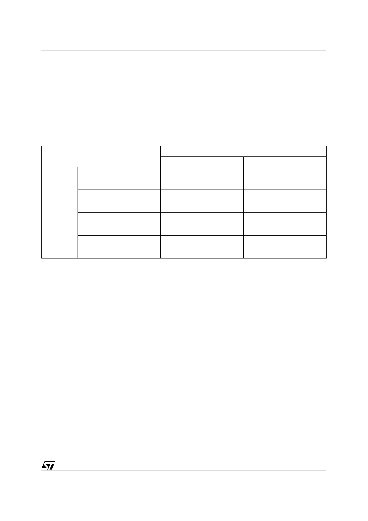
Table 1. Forward and Backward Compatibility: Lead-frame Based Components
Lead-frame Based Packages
Leaded component Tin-Lead
finish
Lead-free compon en ts Tin
finish
Supplier
Lead-free compon en ts
NiPdAu finish
Lead-free compon en ts Tin
Bismuth finish
Leaded Solder Lead-free Solder
Today and past
majority of cases
Processability: OK
Solderability: OK
Reliability: OK
Processability: OK
Solderability: OK
Reliability: OK
Processability: OK
Solderability: OK
Reliability: not recommended
Customer
Processability: OK
Solderability: OK
Reliability: OK
Processability: OK
Solderability: OK
Reliability: OK
Processability: OK
Solderability: OK
Reliability: OK
Processability: OK
Solderability: OK
Reliability: OK
Processability
Components are warranted to withstand the soldering temperatures required for soldering them with standard alloys (SnPb) and with Lead- free alloys (SnAgCu) . Jedec/IPC stand ard J-STD020 is the refer ence
standard used to ensure the soldering resistance of components.
■ For reflow soldering: paste application and component placement do not require specific actions
■ For wave soldering: glue application, component placement and glue cure do not require specific
actions
■ The main differences in the soldering process are time and temperature (both of which are higher
when using lead-free solder pastes)
International standards for the soldering resistance of components, such as IPC/ JEDEC J-STD020,
should not be confused with the required profiles for the soldering of components on board.
The aim of the soldering resistance profile is to describe the maximum heat that components have to withstand during soldering. The soldering process is possible at lower temperatures: see Table 2.
3/9
Page 4

AN2034 - APPLICATION NOTE
Table 2. Minimum and Recommended Profiles For Convection Reflow Soldering
Convection Reflow Profile
Lead solders (SnPb) 210°C 20 seconds 220°C – 30 seconds
Lead-free solders
(SnAgCu)
Minimum Peak
Temperature
235°C 20 seconds 245°C – 30 seconds
Minimum Time Above
Liquidus Of Sol d er Pa st e
Materials
Lead-frame Package Soldering Processes
The soldering process for Copper lead-frames wit h NiPdAu coatings incl udes the wetting of surfac e by
molten solder, the dissol uti on o f Pd and Au th in lay ers in th e s old er and the cr eati on of an SnN i in ter me tallic layer by diffusion.
The soldering proce ss fo r Copp er an d A ll oy 42 lea d-f rame s with Tin-Lead co ating i nc lu des th e m elt ing of
the solder paste and of the thin solder coating on connections, wetting and soldering by diffusion, with the
subsequent creation of an intermetallic layer (NiSn or CuSn).
The soldering process for Copper and Alloy42 lead-frames with Tin coating includes the melting of the solder, wetting on the Tin coated connection and, as a result of the quick diffusion process, the melting of the
coating layer, and th en soldering by diffusion leading to the creation of an intermetall ic layer (NiSn or
CuSn).
The preheating and the length of th e typica l conve ction reflo w profile re sult in n o major diff erence wh en
soldering Tin plated or Tin-Lead plated components.
Recommended Peak
Temperature And Time
Above Liquidus
Lead-frame Package Solderabil ity
Sn- and NiPdAu- coated surfaces are solderable with SnPb and Lead-free solder pastes. Refer to the Application Note AN2036 on solderability.
Lead-frame Package Solder Joint Reliability
Tin-Bismuth coated units soldered with Tin-Lead may show unstable solder joint reliability due to the very
low melting eutectic of Tin-Bismuth-Lead (92°C).
The use of TinBis muth c oat ing wi th st anda r d L ead ed so lde r al loys i s not rec omm end ed. It may however
be validated by the custo mers for specific applica tions.
The solder joint reli ability of com ponents wit h Tin and NiPd Au coatin gs has been shown to be simil ar or
better than that of components with Tin-lead coating.
Thermal Cycling has bee n us ed as a reli abi li ty tes t fo r sol der j oi nt b ec aus e it c aus es th ermo- m ech ani c al
solder fatigue and it is a good simulation tool for the long term reliability of electronic systems.
4/9
Page 5

AN2034 - APPLICATION NOTE
Figure 1. Example of Weibull Failure Analysis after Thermal Cycling of Lead-free and Leaded
Soldered Boards with Sn plated TQFP100 Components (−40/+125°C) (Cu-based lead- frame)
Note: 1. T he source is Philips Semiconductors.
5/9
Page 6

AN2034 - APPLICATION NOTE
BGA PACKAGE COMPATIBILITY
Again, three new cases need to be considered (as summarized in Table 3.), o n top of t he pres ent situat ion,
with the supplier supplying leaded components, and the customer using leaded solder:
■ Customers who use leaded solder on lead-free components (backward compatibility)
■ Customers who use lead-free solder (and a 30 to 40°C higher soldering temperature) on leaded
components (forward compatibility)
■ Customers who use lead-free solder on lead-free components
The main problem is with the second new case: the customer who uses leaded solder on lead-free
components. Reliabi li ty is all ri ght , and e ve n an i mprov em ent o n usin g SnPb solder; but proces sa bi li ty is
a critical issue, due to the lo w temperature used (2 15°C, instead of the 235°C that the package was
designed to work with).
Table 3. Forward and Backward Compatibility: BGA Components
BGA packages using laminated
substrates
Leaded component TinLead Balls
Supplier
Lead-free compone nts
Tin Silver Copper balls
Leaded Solder Lead-free Solder
Today and past majority of cases
Processability: critical
Solderability: OK
Reliability: critical If solder joints
temperature is below 230°C
Customer
Processability: OK
Solderability: OK
Reliability: OK
Processability: OK
Solderability: OK
Reliability: OK
BGA Package Processability
In the case of lead-free BGA-packages the soldering temperature must be above 230°C for processability
and joint reliability. This is because a different temperature at the balls leads to different mounting heights
(see Figure 2.). Low BGA soldering temperature may also result in poor joint uniformity (see Figure 3.).
Figure 2. Effect Of Soldering Temperature On Joint Height
Note: 1. The source is Infineon Technologies.
6/9
Page 7

Figure 3. Mounted Lead-free Solder Balls
AN2034 - APPLICATION NOTE
With SnPb solder
low temperature
With SnPb sol der
above 230°C
With Lead-free
SnAgCu solder
BGA Package Solderability
The solderability of BGA components with Leaded or Lead-free balls is equivalent.
BGA Package Solder Joint Reliability
Lead-free solder joint reliability, versus thermal cycling, is improved compared to SnPb balls.
Figure 4. Weibull Failure Analysis after Thermal Cycling of lead-free and lead-containing reflow
solder TFBGA6x6-46 with 0.4mm solder balls (both SnPb-SnAgCu)
4 tested processes using -40°C/
+125°C thermal cycling and continuous electrical re sis tan ce m on itor ing of
daisy chain units
SnPb balls + SnPb paste (220°C)
SnAgCu balls + SnPb paste (220°C)
SnAgCu balls + SnA gC u p as t e ( 24 5°C )
SnAgCu balls + SnA gC u p as t e ( 25 0°C )
7/9
Page 8

AN2034 - APPLICATION NOTE
CONCLUSION FOR COMPATIBILITY
STMicroelectronics components, lead-free or leaded, are fully compatible, from the soldering process, and
quality and reliability stand-points, with both lead-free or leaded solder pastes.
The only exception is for lead-free BGA using leaded solder process (since the reflow temperature could
be too low for melting the lead-free solder balls).
Otherwise, all lead- free package dimen sions, and their mechanical an d electrical beha viors, are simila r
for the lead-free and leaded components.
REVISION HISTORY
Table 4. Document Revision History
Date Version Revision Details
08-Nov-2004 1.0 First Issue
8/9
Page 9

AN2034 - APPLICATION NOTE
Information furnished is be lieved to be a ccur ate and reli able. Howe ver, STMicroele ctronic s assu mes no r esponsib ilit y for th e consequences
of use of such information nor for any infrin gement of patent s or other rights of third parties which ma y result from it s use. No license is granted
by implication or otherwi se under any patent or patent rights of STMicroelectronics. S pecifications mentioned in this publication are subject
to change without not ice. This pub licat ion su persed es and repl aces all in format ion previou sly su pplie d. STMicroele c tronic s prod ucts ar e no t
authorized for use as critical compone nts in life support devices or systems witho ut express written approval of STMicroelectronics.
The ST logo is a registered trademark of STMicroelectronics.
All other names are the property of their respective owners
© 2004 STMicroelectronics - All rights reserved
Australia - Belgium - Brazil - Canada - China - Czech Republic - Finland - France - Germany - Hong Kong - India - Israel - It aly - Japan -
Malaysia - Malta - Morocco - Singapore - Spain - Sweden - Switzerland - United Kingdom - United States of America
STMicroelectronics group of companies
www.st.com
9/9
 Loading...