

Page 1

AN2031
APPLICATION NOTE
STA308-508
EVALUATION BOARD DESCRIPTION
1 DESCRIPTION
The STA308A is a single chip solution for digital audio processing and control in multi-channel
application.
It provides output capabilities for DDX (Direct Digital Amplification). In conjunction with DDX
power device, it provides high quality, high efficiency, all digital amplification.
STA508 is a monolithic quad half bridge stage in Multipower BCD technology. The device can
be used as dual bridge or reconfigured, by connecting CONFIG pin to V
with double current capability.
This device is particularly designed to make the Output stage of a stereo DDX amplifier capable to deliver 80 + 80W @THD = 10% at V
In single BTL configuration, is also capable to deliver a peak of 160W@THD = 10% at V
35V on 4Ω load (t<= 1sec).
= 35V output power on 8Ω load.
cc
2 STA308-508// EVALUATION BOARD DESCRIPTION
In this board it is possible to solder STA308 or STA308A device how digital audio processor.
There are three jumpers (JP2, JP3, JP6) to select the correct device.
The board has one S/PDIF input (electrical single ended and optical).
In this board it is possible to use two different powers (10V to 35V on J2) and logic (5V on J1)
stages or only one supply (10V to 35V on J2) for both stages. This feature is possible setting
JP1 in EXT-SEL or INT-SEL respectively.
U6 and U7 are configured to drive 3 or 2 ohm (over 250W) on the channel.
pin, as single bridge
dd
cc
=
2.1 SUPPLY VOLTAGE, REGULATORS
The STA308-508// board uses 5V, 3.3V power regulation for logic circuitry and 10<V
power section of STA508 device.
It is possible to apply only one power supply and to extract the logic power supply utilizing the
L4971D step down device
2.2 S/PDIF INPUT INTERFACE
The STA308A controller's data interface is serial I
The STA308-508//-EVB input accommodates coaxial or optical S/PDIF digital audio interfaces
using a digital audio receiver IC. Jumper JP5 may select either input. S/PDIF interfaces
(STA120D) will support sample rates from 32KHz to 96KHz
Optical S/PDIF receiver IC is SHARP GP1F31R.
2.3 DIGITAL SIGNAL PROCESSING
The STA308A converts pulse code modulated, PCM, digital audio input signals into PulseWidth Modulated PWM. This signal enters in the same time in the two STA508 ICs and the exit
signal is at high level of power. The STA308A has two independent volume control registers
AN2031/0705
2
S for input.
<35 for
cc
Rev. 1
1/12
Page 2

AN2031 APPLICATION NOTE
that have an adjustment range from +48dB to -78dB in 0.5dB increments. In addition, the mater volume is adjustable from 0dB to -127dB in 0.5dB steps.
Tone control registers boost or cut the treble and bass by +/-12dB, in 2dB steps.
EQ filters are IIR biquads configurable by programmable coefficients.
2.4 POWER OUTPUT
The power level signals are applied to passive two-pole low pass filter, and provide low distortion audio power to the load. The output filter functions to prevent unwanted high frequency
switching signals from reaching the load. Filter designs for 2Ω. Peak voltage on power pins
must not exceed 35V.
Snubber networks are employed to protect the output MOSFETs from inductive transients,
which can reach levels higher than the supply voltage.
Output snubber filter values are R18/C66 and R14/C53.
The other critical components for device reliability are C47, C51, C58, C63 (1uF) and C48,
C52, C59, C64 (100nF); these bypass capacitors from Vcc and power GND pins of STA508.
These capacitors must be X7R Ceramic or Tantalum SMD construction and must be located
as close as possible to the device pins.
The STA508 shuts down when it reaches 150°C.
2.5 JUMPERS CONNECTOR
The STA308-508//-EVB provides some jumpers to configure the board.
2.5.1 JUMPERS:
JP1: (INT-SEL-EXT): short on EXT-SEL to use different power supplies; short on INT-SEL to
use only one power supply;
JP2: (2.5A): short (with solder tin) if STA308 IC is solder on the board. If there is the STA308A
this jumper could be opened;
JP3: (2.5A): short (with solder tin) if STA308 IC is solder on the board. If there is the STA308A
this jumper could be opened;
JP4: short this jumper to use two different power supply;
JP5: (OPTIC- SPDIF -ELEC): short the central pin with ELEC pin to use Electric S/PDIF; short
the central pin with OPTIC pin to use the optical S/PDIF.
JP6: short (with solder tin) 3.3A and center if STA308A IC is solder on the board. If there is the
STA308A this jumper could be short on 3.3V and center
JP7: this pin must be open.
2.5.2 CONNECTORS:
J1: Logic supply (5V)
J2: Power Supply (10V to 35V)
J3: Male 20 pin connector for plug control board
J4: RCA connector electric S/PDIF
J5: Optical S/PDIF SHARP GP1F31R
J6: Connector for output load A
2/12
Page 3
AN2031 APPLICATION NOTE
3 CONFIGURE STA308A-508//-EVB WITH LPT INTERFACE
1) Plug the LPT Interface on the board utilizing J3 of STA308A-508//-EVB and J2 of LPT Interface;
2) Connect PC parallel port to the LPT board using a parallel cable;
3) Select S/PDIF Input mode (electric or optical) with JP5;
4) Connect logic supply (+5V) on J1 and power supply [10V..35V] on J2;
5) Connect output load on J6;
6) 6Turn on the board;
7) Run STA308A-508PControlPanel.exe on the PC.
3.1 Configuring GUI Software:
1) Go to "Registers" page on GUI.
2) Click "AutoFind LPT" button. It appears the number of LPT port (0x278 or 0x378);
3) Click "Reset" button
4) Click "Power Up" button
5) Click "Test Board I/O". If "passed" it is OK. If "failed", then perform manual board-reset by press-
ing SW1 button and try again. If still "failed" then make sure connections are OK.
6) Go to "Control" page on GUI.
7) Click "Ext Amp Power Up" to enable the output power.
8) Increase "ALL" master volume control.
4 PERFORMANCES
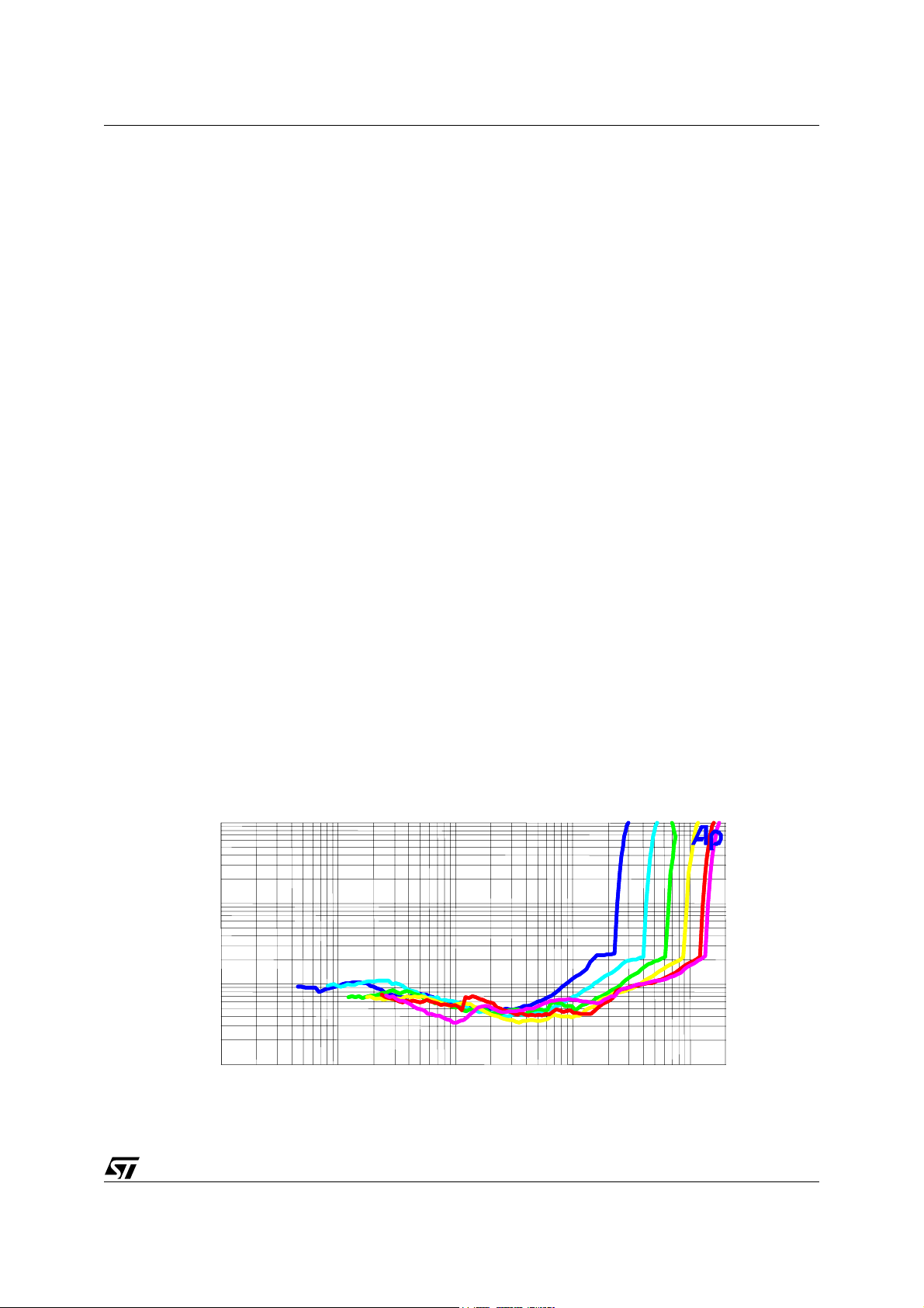
4.1 THD+Noise Ratio versus Output Power at different input power supply Input
frequency: 1KHz; Output load: 4Ω;
Blue: 15V; Cyan: 20V; Green: 25V; Yellow: 30V; Red: 35V; Magenta: 37V
Figure 1. Audio Precision
10
10
5
5
2
2
1
1
0.5
0.5
%
%
0.2
0.2
0.1
0.1
0.05
0.05
0.02
0.02
0.01
0.01
10m 20020m 50m 100m 200m 500m 1 2 5 10 20 50 100
10m 20020m 50m 100m 200m 500m 1 2 5 10 20 50 100
W
W
3/12
Page 4
AN2031 APPLICATION NOTE
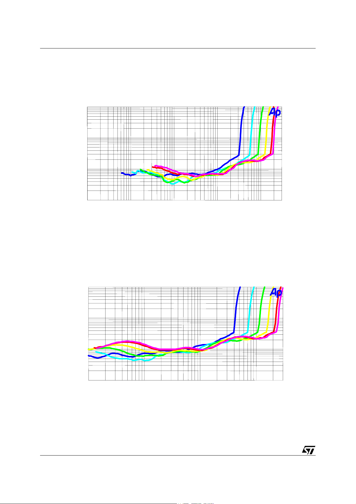
4.2 THD+Noise Ratio versus Output Power at different input power supply Input
frequency: 1KHz; Output load: 2.67Ω;
Blue: 15V; Cyan: 20V; Green: 25V; Yellow: 30V; Red: 35V; Magenta: 37V
Figure 2. Audio Precision
10
10
5
5
2
2
1
1
0.5
0.5
%
%
0.2
0.2
0.1
0.1
0.05
0.05
0.02
0.02
0.01
0.01
10m 30020m 50m 100m 200m 500m 1 2 5 10 20 50 100
10m 30020m 50m 100m 200m 500m 1 2 5 10 20 50 100
W
W
4.3 THD+Noise Ratio versus Output Power at different input power supply Input
frequency: 1KHz; Output load: 2Ω;
Blue: 15V; Cyan: 20V; Green: 25V; Yellow: 30V; Red: 35V; Magenta: 37V
Figure 3. Audio Precision
10
10
5
5
2
2
1
1
0.5
0.5
%
%
0.2
0.2
0.1
0.1
0.05
0.05
0.02
0.02
0.01
0.01
100m 300200m 500m 1 2 5 10 20 50 100
100m 300200m 500m 1 2 5 10 20 50 100
W
W
4/12
Page 5

AN2031 APPLICATION NOTE
4.4 THD+Noise Ratio versus frequency at different output power Input power supply:
25V; Output load: 4Ω;
Blue: 0dB; Cyan: -10dB; Green: -20dB;
Figure 4. Audio Precision
1
1
0.5
0.5
0.2
0.2
0.1
0.1
%
%
0.05
0.05
0.02
0.02
0.01
0.01
20 20k50 100 200 500
20 20k50 100 200 500
Hz
Hz
1k
1k
2k 5k 10k
2k 5k 10k
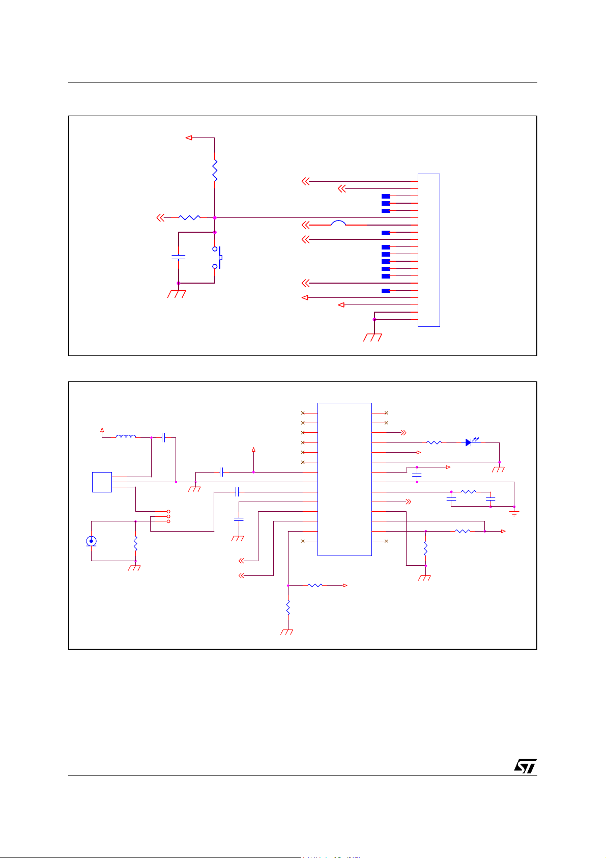
5 SCHEMATIC AND LAYOUT
5.1 Schematic
Figure 5. Power Section
J1
2
GND
1
Logic
+5V
Vcc
LCL
J2
1
Pwr
C6
100n
2
GND
+30V
132
L2
+
C8
C9
10u 50V
220n 50V
R1 10K
C1 100n
89
U1
7
10
78910
6
11
6
11
5
12
5
12
4
13
4
13
3
14
3
14
2
15
2
15
R3
9.1K
C12
22n
1
16
1
16
L4971D
Ext
5V SEL
Sel
Int
JP4
C10
100n
1 2
JUMPER
JP1
1
2
3
L1 220u 3V3
R2
2.7K
D1
SMS160
R4
C11
2.2n
4.7K
+
100u 10V
5V
LD1086DT33
U2
23
OUTIN
C2
+
C3
330u 10V
C14
100n
GND
1
LD1086DT25
U3
23
OUTIN
GND
1
JP3
2V5
C15
100n
Vicino all'STA308
2A5
JP2
2A5
1 2
L5FERRIT E
C16
100n
L6FERRIT E
3A3
2V5
L3
FERRITE
C4
10u 10V
1 2
C5
100n
L4FERRITE
+
C7
100n
+
C13
10u 10V
5/12
Page 6
AN2031 APPLICATION NOTE
Figure 6. Connection Section
3V3
R2 0 33
RES ET
13
C1 7
1n
R5
10K
SW1
BUTTON
SCL
EAPD
PWDN
TH_W
3V3
SDA
1 2
JP7
5V
TP1
TP2
TP3
TP4
TP5
TP6
TP7
TP8
TP9
TP10
J3
1
2
3
4
5
6
7
8
9
10
11
12
13
14
15
16
17
18
19
20
CON 20
Tes t Poi nt er
Tes t Poi nt er
Tes t Poi nt er
Tes t Poi nt er
Tes t Poi nt er
Tes t Poi nt er
Tes t Poi nt er
Tes t Poi nt er
Tes t Poi nt er
Tes t Poi nt er
Figure 7. S/P DIF Section
5V
J4
GP1F31R
+VS
GND
DAT A
J5
RCA J ACK
FERRI TE
1
2
3
C18 100n
L7
JP 5
SPDT/SM
1
OPT
2
-
3
ELEC
R9
82
C19 100n
100n
LRCKI SPDIF
BICKI S PDIF
C21 100n
C2 4
U4
1
C
2
Cd/F 1
3
Cc/F0
4
3V3
Cb/E2
5
Ca/E1
6
C0/E0
7
VD+
8
DGND
9
RXP
10
RXN
11
FS YNC
12
SCK
13
CS1 2/FCK
14 15
UCBL
STA120
R1 1 0
R1 2
NON Salda re
3V3
VERF
Ce/F2
SDATA
ERF
VA+
AGND
FI LT
MCK
SEL
28
27
26
25
24
M1
23
M0
22
21
20
19
18
M2
17
M3
16
DAT A SPDIF
R6 560
3V3
C2 0
100n
XTI SP DIF
R10
NON s aldare
Non Saldare
D2
3A3
C22
15n
R8 0
R7330
C2 3
470n
3V3
6/12
Page 7

Figure 8. STA308A Section
AN2031 APPLICATION NOTE
3V3
2V5
PWDN
1
C40
100p
2
3
4
5
6
7
8
9
10
11
12
13
14
15
16
2A5
MVO
TES T_M ODE
Vdd3
GND
Vdd
SDI_78
SDI_56
SDI_34
SDI_12
LRCKI
BICKI
Vdd3
GND
Vdd
RESET
PLL_BYPASS
C29
RESET
100n
C31
100n
C33
100n
C35
100n
SDA
SCL
XTI SPDIF
DATA SPDIF
LRCKI SPDIF
BICKI SPDIF
R13
3.3K
C42
1n
3V3
2V5
3V3
2V5
C25
100n
C28
100n
64
Vdd
PWDN
SDO_56
SDO_78
SA
SDA
SCL
XTI
171819202122232425262728293031
C39
100n
Vdd
Vdd3
GND
BICKO
LRCKO
SDO_12
SDO_34
U5
STA308
FILTER_PLL
VddA
GNDA
Vdd3
CKOUT
Vdd
GND
2V5
C41
100n
PWR PLL
C26
100n
Vdd3
GND
EAPD
Vdd3
OUT8B
OUT8A
C38
100n
C37
100n
2V5
3V3
C27
100n
PWM1A
TP11
PWM1B
495051525354555657585960616263
OUT1B
OUT1A
OUT7B
48
OUT2A
47
OUT2B
46
Vdd
45
GND
44
Vdd3
43
OUT3A
42
OUT3B
41
OUT4A
40
OUT4B
39
OUT5A
38
OUT5B
37
Vdd
36
GND
35
Vdd3
34
OUT6A
33
OUT6B
OUT7A
32
3V3
PWM2A
PWM2B
PWR PLL
TP1 2
2
EAPD
C30
100n
C32
100n
C34
100n
C36
100n
13
JP6
JUMP ER SOLDE R
2V5
3V3
2V5
3V3
NUOVO
3A3
3V3
7/12
Page 8

AN2031 APPLICATION NOTE
Figure 9. STA508 Section
EAPD
C61
100n
C49
100n
C55
100n
PWM2A
PWM2B
D4 1N4148
C62
100n
C44
100n
PWM2 A
PWM2 B
D3 1N4148
C50
100n
FT500
100n
TH_ W5 00
TH _W
3V3
C60
R15 10K
R16 10k
3V3
TH _W5 00
FT500
EAPD500
EAPD500
3V3
C54
100n
TP1 3
TP1 4
C43
100n
36
35
34
33
32
31
30
29
28
27
26
25
24
23
22
21
20
VccSig
VccSig
Vss
Vss
IN2B
IN2A
IN1B
IN1A
TH_W ARN
FAULT
TRIST ATE
PWRDN
CONFIG
Ibias
Vdd
Vdd
GNDReg
36
35
34
33
32
31
30
29
28
27
26
25
24
23
22
21
20
VccSig
VccSig
Vss
Vss
IN2B
IN2A
IN1B
IN1A
TH _WA RN
FAULT
TR IST ATE
PWRDN
CONFIG
Ibias
Vdd
Vdd
GNDR eg
GND Sub
OUT2B
OUT2B
Vcc2B
GND2B
GND2A
Vcc2A
OUT2A
OUT2A
OUT1B
OUT1B
Vcc1B
GND1B
GND1A
Vcc1A
OUT1A
OUT1A
STA505
GND Sub
OUT2B
OUT2B
Vcc2B
GND2B
GND2A
Vcc2A
OUT2A
OUT2A
OUT1B
OUT1B
Vcc1B
GND1B
GND1A
Vcc1A
OUT1A
OUT1A
STA505
U7
1
OUT1A
2
3
4
5
6
7
8
OUT1A
9
OUT1B
10
11
12
13
14
15
16
OUT1B
17
1819
NCGNDClean
U6
1
2
OUT1A_
3
4
5
6
7
8
9
OUT1A_
10
OUT1B_
11
12
13
14
15
16
OUT1B_
17
1819
NCGNDC lean
C58
1u
C63
1u
C47
1u
C51
1u
C56
100n
C59
100n
C64
100n
C45
100n
C48
100n
C52
100n
+
+
Vcc
C57
1000u 50V
C46
1000u 50V
Vcc
Figure 10. Output Filter Section
L10
C66
330p
R18
20
L11 22u
22u
OUT1A_ C65
OUT1B_
L8 22u
C53
330p
R14
20
L9 22u
OUT A 505
OUT B 505
OUT 1A
OUT 1B
8/12
100n
C68
100n
C71
100n
C73
100n
R17
6.2
R19
6.2
C69
1uF 63V
C67
1n
C72
1n
C70
1nF 63V
J6
1
2
CON2
OUTA 505
OUTB 505
Page 9
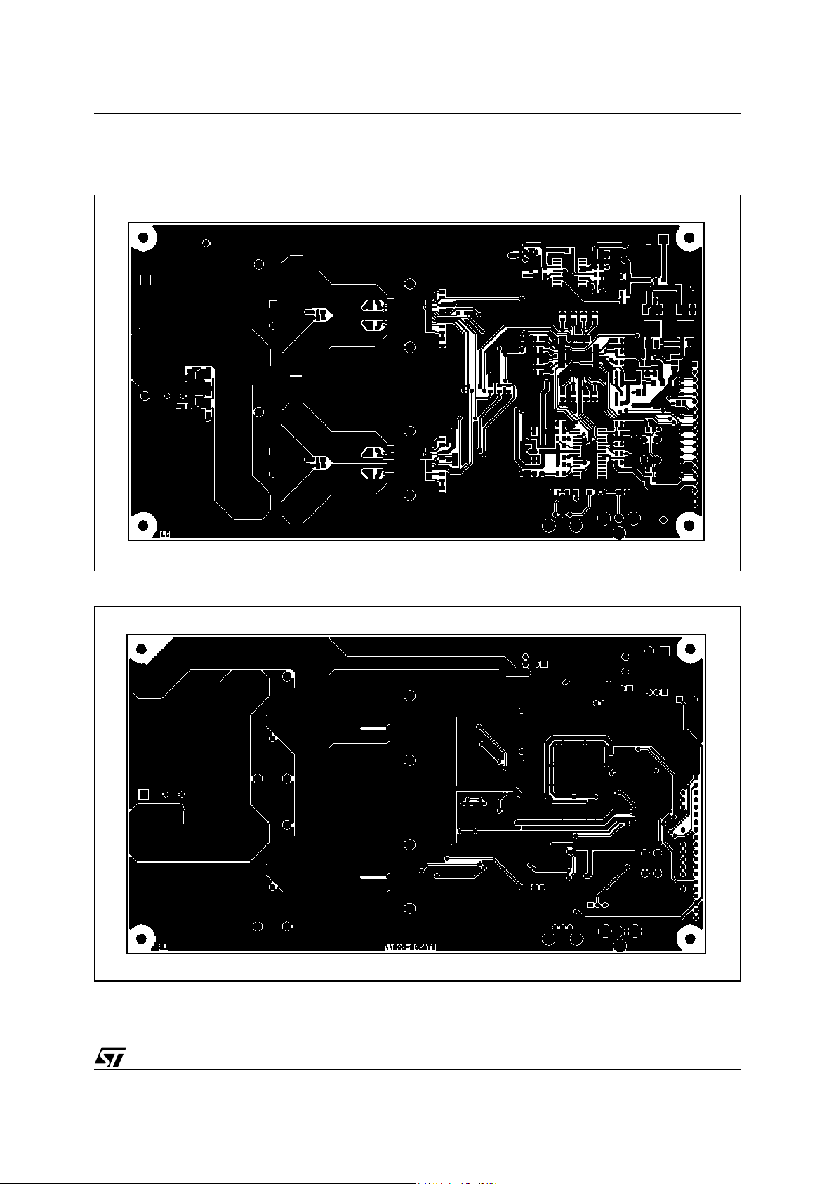
5.2 Layout
Figure 11. Component Layer
AN2031 APPLICATION NOTE
Figure 12. Solder Layer
9/12
Page 10

AN2031 APPLICATION NOTE
Figure 13. Serigraphy
10/12
Page 11

Table 1. Revision History
Date Revision Description of Changes
July 2005 1 First Issue
AN2031 APPLICATION NOTE
11/12
Page 12

AN2031 APPLICATION NOTE
The present note which is for guidance only, aims at providing customers with information regarding their products in
order for them to save time. As a result, STMicroelectronics shall not be held liable for any direct, indirect or
consequential damages with respect to any claims arising from the content of such a note and/or the use made by
customers of the information contained herein in connection with their products.
Information furnished is believed to be accurate and reliable. However, STMicroelectronics assumes no responsibility for the consequences
of use of such information nor for any infringement of patents or other rights of third parties which may result from its use. No license is granted
by implication or otherwise under any patent or patent rights of STMicroelectronics. Specifications mentioned in this publication are subject
to change without notice. This publication supersedes and replaces all information previously supplied. STMicroelectronics products are not
authorized for use as critical components in life support devices or systems without express written approval of STMicroelectronics.
The ST logo is a registered trademark of STMicroelectronics.
All other names are the property of their respective owners
© 2005 STMicroelectronics - All rights reserved
Australia - Belgium - Brazil - Canada - China - Czech Republic - Finland - France - Germany - Hong Kong - India - Israel - Italy - Japan -
Malaysia - Malta - Morocco - Singapore - Spain - Sweden - Switzerland - United Kingdom - United States of America
STMicroelectronics group of companies
www.st.com
12/12
 Loading...