

Page 1

AN2025
®
APPLICATION NOTE
Converter Improvement Using
Schottky Rectifier Avalanche Specification
STMicroelectronics gives in product datasheets useful information for all their Schottky Rectifier families
to define their working limit in the avalanche area. A simple method to determine if a Schottky diode can
work in the avalanche area in a given Switch Mode Power Supply (SMPS) is described in this document.
Then an accurate method will be defined in order to estimate the maximum average avalanche power
losses. Finally, a concrete example will be illustrated to show how the choice of a Schottky diode can be
optimized in order to improve the efficiency of the converter.
I. Introduction
The design of SMPS is subjected to heavy constraints in order to improve the trade-off between the cost
and the power density. One way to respond to these aggressive specifications is to drive components
closer to their intrinsic limits. The use of Schottky diodes in the avalanche area is a good example of this
evolution.
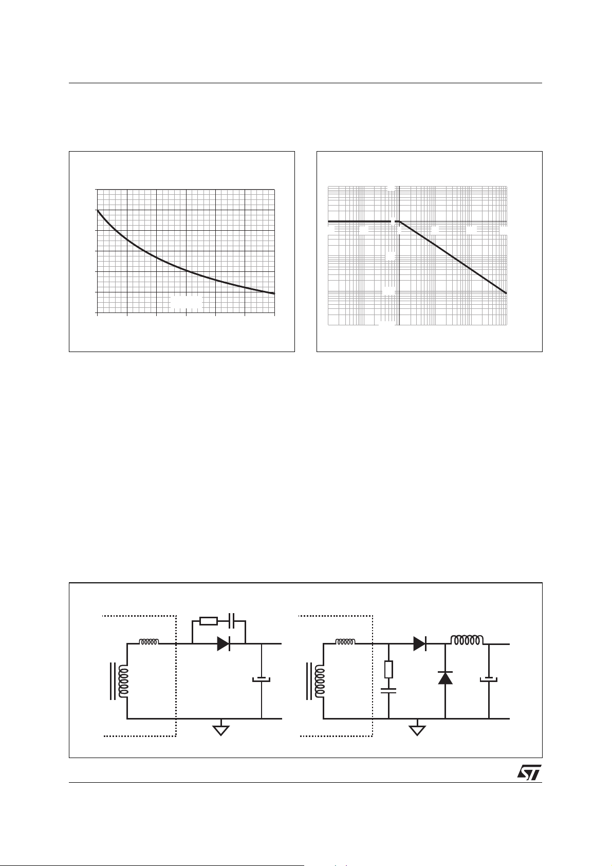
II. Description of the specification tool
STMicroelectronics guarantees for each Schottky diode a reference avalanche power capability corresponding to a rectangular current pulse: P
(1µs, 25°C) (given at tp=1µs and Tj = 25°C) - See figure 1.
ARM
Derating curves shown in figure 2 and figure 3 give
the admissible avalanche power for each Schottky
diode versus the operating junction temperature
(T
) and the pulse duration (tp).
j
P
(1µs,25°C) for each part number as well as
ARM
derating curves are given in the respective data
sheet.
The designer must ensure that the guaranteed avalanche power P
alanche power in the application P
P
AVALANCHE
ARM (tp,Tj
(application) < P
) is greater than the av-
AVALANCHE
(tp, Tj)
ARM
:
Figure 1: P
avalanche power)
(1µs, 25°C) (Maximum repetitive
ARM
SCOPE
V
Clamp
I
PP
P (1µs, 25°C) = V
ARM Clamp PP
t = 1µs
p
T = 25°C
j
x I
REV. 1AN2025/1004
1/11
Page 2
AN2025 - APPLICATION NOTE
Figure
1.2
1
0.8
0.6
0.4
0.2
0
P
ARMtpTj
-------------------------------------------- -
2: Figure 3:
P
ARMtp
P(t,T) /
ARM p j
25 50
,()
versus T
25oC
,()
P (t , 25°C) versus T
ARM p j
T (°C)
j
75
100 125 150 175
j
P
---------------------------------------- -
P
P(t,T) /
ARM p j
0.01 0.1 1 10 100 1000
tpT
ARM
ARM
,()
j
1µsT
P (1µs, T , 25°C) versus t
ARM j p
10
1
0.1
0.01
0.001
versus T
,()
j
p
t (µs)
p
III. Simple method to estimate the maximum avalanche peak power
III.1. Setting the Problem
Most of the time, it is difficult to accurately determinate the avalanche power through the diode in the hardware circuit.
This is mainly due to measuring problems such as delay time between current and voltage probe, the very
low pulse duration and the snubber circuit impact. Generally, in SMPS applications, the maximum
avalanche peak power occurs for a diode having the lowest clamping voltage. Practically, this diode is very
difficult to find.
These are the reasons why STMicroelectronics proposes a simple method to estimate the maximum avalanche peak power P
> P
AVALANCHE
) but sufficient to determine whether or not a given Schottky diode will sustain the applied
PEAK_AV
. In most of SMPS applications, this method will be pessimistic (P
PEAK_AV
avalanche energy. This method only covers Schottky diodes used in rectification function for SMPS (see
figure 4), where the pulse duration of the avalanche current t
is less than 1µs.
p
Figure 4: Typical secondary rectification topologies
R
C
S
S
L
F
or
L
F
D
R
R
S
C
S
D
F
Transformer Transformer
2/11
Page 3
AN2025 - APPLICATION NOTE
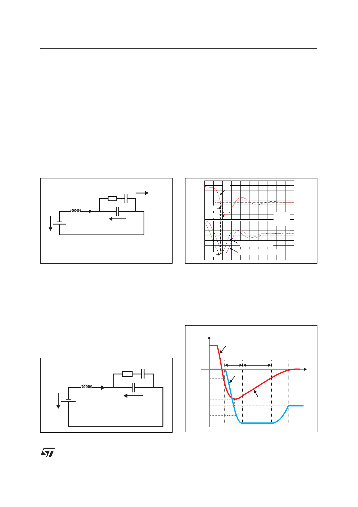
III.2. Switching-off analysis (simple method)
III.2.1. Introduction
The figure 5 shows the equivalent circuit that can be used to simulate a secondary rectification function
when the diode turns off : L
by the capacitance Cj, R
The figure 6 shows the corresponding current and voltage waveforms taking into account the delay time
between current and voltage probes. When the total current (current in the diode + current in the snubber)
is at maximum (I
PEAK
voltage across the diode is equal to V
represents the leakage inductance of the transformer. The diode is modelized
F
and CS are the snubber components.
S
), the voltage across the leakage inductance is zero (dIT/dt = 0). Consequently the
.
S
i
T
= I
PEAK
⇔ vD = -V
S
Figure 5: Basic equivalent circuit
Figure 6: Total current (iT) and voltage (VD)
when the diode turns off
v
RRM
SPIKE
D
i with delay time
T
i without delay time
T
C
S
R
S
L
iT
F
V
S
L : leakage inductance of the transformer
F
C
j
v
D
Snubber
-VS
-V
-V
I
PEAK
III.2.2. Switch-off behavior when the diode works in the avalanche area
The figure 7 shows the switch-off behavior when the diode works in the avalanche area.
This characteristic is made up of 2 distinct phases.
Phase 1: t ∈ [t
At t = t
: iT = I
0
0
, t1]
0
Figure 7: Switch-off behavior when the diode
works in the avalanche area
vD,i
T
vD = 0
i
T
20V/div
1A/div
20ns/div
0V
0A
t
t
0
1
C
R
i
L
V
S
T
F
S
S
I
-V
I
PEAK
-V
RRM
Clamp
0
I
1
-V
S
C
j
v
D
v
D
t
Phase2Phase1
dI
2
t
/dt
T
3/11
Page 4
AN2025 - APPLICATION NOTE
The first phase corresponds to the charging of the junction capacitance of the diode, Cj.
The voltage across the diode V
figure 7). As was explained above, when the total current is equal to I
Once the current has reached I
(see figure 7).
decreases until it reaches the clamping voltage of the diode -V
D
, it then increases to reach the value I1 corresponding to VD = -V
PEAK
, VD is equal to -VS.
PEAK
Clamp
(see
Clamp
Phase 2: t ∈ [t
At t = t
: iT = I
1
vD = V
1
1
, t2]
Clamp
C
S
S
i
AVALANCHE
R
i
L
T
F
V
S
V
Clamp
During this phase, the diode works in the avalanche region. Consequently, the voltage across
the diode is equivalent to a voltage generator
equal to V
Clamp
.
The total current increases linearly with a slope
equal to:
di
After t
V
T
--------
=
----------------------------
dt
, the voltage across the diode increases towards -VS (see figure 7).
2
Clamp
L
F
Vs
(see figure 7)
These considerations show that:
I
< I
1
PEAK
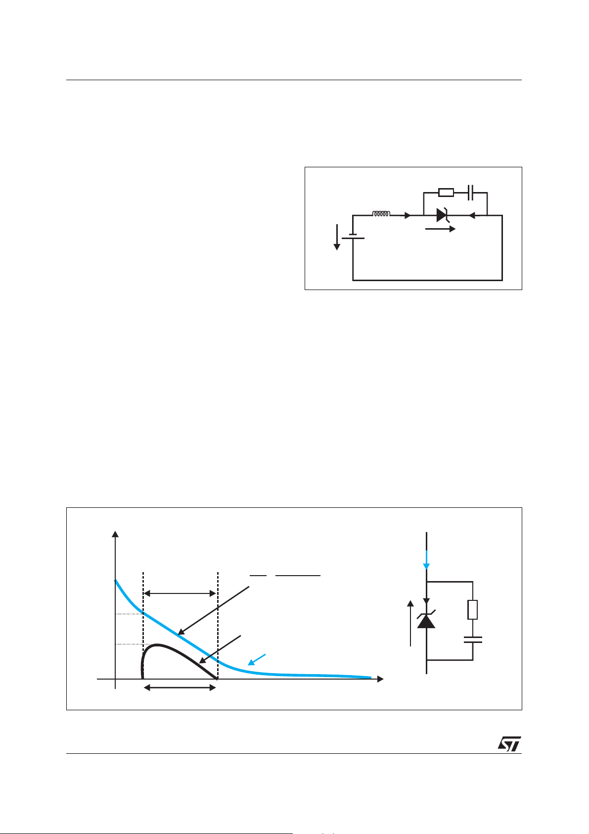
III.2.3. Estimation of the maximum avalanche peak power: P
PEAK_AV
The figure 8 shows in blue color the total current IT (diode + snubber) and in black line the real avalanche
current waveforms during the switching-off of the diode.
Figure 8: Total current and avalanche current waveforms when the diode works in the avalanche area
Clamp
Phase2
i
T
R
S
C
S
I
PEAK
I
AR
I
V-V
di
Phase2
I
1
i
AVALANCHE
dt
Clamp
T
=
i
T
S
L
F
i
AVALANCHE
V
t
t
2
4/11
t
1
t
< 1µs
p
Page 5

AN2025 - APPLICATION NOTE
The real peak current in avalanche (IAR) is less than I1 and I1 is less than I
avalanche current value by taking I
for all further calculations.
PEAK
. We first approximate an
PEAK
Moreover, STMicroelectronics guarantees that the maximum clamping voltage of Schottky diodes is always less than 2×V
RRM
(V
: Maximum repetitive reverse voltage).
RRM
Consequently from these 2 conditions, a conservative estimation of the maximum avalanche peak power
can be done:
P
AVALANCHE
= IAR.V
Clamp
< P
PEAK_AV
= I
PEAK
.(2×V
RRM
)
Finally, to determine if a given Schottky diode can work in the avalanche area in a given SMPS, the following condition must be respected:
2.I
PEAK.VRRM
< P
ARM
(1µs,Tj)
III.3. Methodology
Here below are the three steps to follow in order to define P
P
(1µs,Tj).
ARM
■ Step1: Total current measurement i
⇒ I
PEAK
■ Step2: Maximum avalanche peak power estimation
⇒ P
PEAK_AV
■ Step3: Check that:
⇒ P
PEAK_AV
[As tp < 1µs ⇒ P
= 2.I
< P
ARM
PEAK.VRRM
(1µs, Tj) using the specification tool (see § II)
ARM(tp
(with snubber)
T
, Tj) = cst = P
ARM
(1µs, Tj)]
PEAK_AV
and to then compare it with
Example:
In this example, a 16A-100V Schottky diode (STPS16H100CT) working in the avalanche area is
considered.
■ Step1:
The figure 9 shows the total current through both
Figure 9: Total current i
(diode + snubber)
T
the snubber circuit and the STPS16H100CT.
■ Step2:
P
PEAK_AV
■ Step3:
is given by:
⇒ P
PEAK_AV
⇒ P
PEAK_AV
= 4.4 x (2 x 100)
= 880W
i
T
t < 1µs
p
2A/div
0.1µs/div
The data sheet of the STPS16H100CT gives:
P
(1µs, 25°C)
ARM
(STPS16H100CT)
= 8700W
With the derating curve figure 2, we get:
I = 4.4A
P
(1µs, 130°C)
ARM
As P
PEAK_AV
(STPS16H100CT)
is lower than P
= 3045W
(1µs, Tj), the
ARM
T = 130°C
j
PEAK
STPS16H100CT can be used safely in this application.
5/11
Page 6

AN2025 - APPLICATION NOTE
IV. Estimation of the average avalanche power losses
The accurate method given below allows the maximum average avalanche power to be determined, and
it can be used to optimize the choice of the diode in order to improve the converter's efficiency. The equivalent circuit during the time the diode works in the avalanche is simulated. From this simulation, the real
avalanche current as well as the pulse duration can be found from which an estimation of the maximum
avalanche energy can be made. The simulation is performed using the Pspice software. The 2 steps that
comprise this method are explained using an adaptor for Notebook as a concrete example (see figure 10).
First step: Measurement
This first step consist of measuring 3 waveforms:
⇒ the total current i
delay time in order to have I
⇒ the voltage across the diode V
⇒ the voltage across the snubber capacitor V
(taking into account the
T
at VD = -VS)
PEAK
D
CS
Figure 11 shows typical waveforms corresponding
to the example.
Figure 11: Waveforms when the diode turns off
V
CS
C
R
S
S
L
F
i
T
V = m.V
S
IN
0 scope
v
D
V
OUT
Figure 10: 70W Adaptor for Notebook, using a
STPS16H100CT in the avalanche
R
C
S
S
STPS16H100CT
P
v
V
D
S
n
S
-V
Clamp_min = -VRRM
-V
SPIKE
V
S
I= 4A
OUT
V = 18V
OUT
0V
0A
i without
T
delay time
i with
T
delay time
I
T0 = 4.2A
I
PEAK
20V/div
1A/div
10ns/div
V
IN
n
V
CS
V = 14V
v
C0
D
The maximum avalanche energy in the diode corresponds to a diode with a minimum clamping voltage
V
Clamp_min
age will be equal to V
equal to V
At v
6/11
. As this value is not given in the data sheet, one can consider that the minimum clamping volt-
. The figure 11 gives the initial conditions when the voltage across the diode is
RRM
D
= V
Clamp_min
RRM
, that is to say V
:iT = iTO = 4.2A
V
CS
= VCO = 14V
RRM
.
Page 7

Second step: Pspice simulation
AN2025 - APPLICATION NOTE
Knowing the initial conditions i
and VCO, the equivalent circuit can be simulated (see figure 12).
TO
The figure 13 shows the simulation results. The result of this simulation is:
t
E
AVALANCHE_max
E
AVALANCHE_max
= 2.5µJ
p
V
=
∫
0
⋅⋅
RRMiAVALANCHE
td
Therefore:
P
AVALANCHE(AVERAGE)max
P
AVALANCHE(AVERAGE)max
= E
AVALANCHE_max
= 250mW
x Fc (with Fc = 100kHz)
This accurate method can be used to estimate the maximum real avalanche peak power in the case where
the estimation with the simple method (cf §III) is too pessimist.
Figure 12: Pspice equivalent circuit with initial conditions I
S
21
L = 280nH
F
1
2
D
and V
TO
R = 47SΩC = 2.2nF
2
i
AVALANCHE
-
1
+
CO
i
SNUBBER
VS
-
+
Figure 13: Simulation results
I = 4.2A
T0
I
AR
V
Clamp_min =VRRM = 100V
V = 14V
C0
i
SNUBBER
V
CS
V = 100V
Clamp_min
E
AVALANCHE_max
t
p
i
T
i
AVALANCHE
= 2.5µJ
7/11
Page 8

AN2025 - APPLICATION NOTE
V. Rectification Schottky diode optimization using avalanche specification
V.1. Changing security margin criteria
The figure 14 shows a typical voltage waveform across a rectification diode. Usually, designers take a conventional security margin between the V
specification of Schottky diodes, this security margin is not required anymore because the diode can work
in avalanche during the turn-off. On the other hand, the new security margin which is an essential condition
to assure the correct working of the power supply is the margin between the maximum voltage V
the new V
RRM
(V
, see figure 14).
RRM2
In the example illustrated here below, a 150V Schottky diode is replaced by a 100V Schottky diode.
max needs to be defined by the designer in the worst case conditions (Vin
V
S
Consequently, the following condition is necessary for V
V
k is a cold start coefficient that is equal to 0.95 in the case where the diode is exposed to very low
temperature (-40°C or -20°C) (for T
> 0°C, k = 1).
j
Figure 14: Voltage across the diode
and the spike voltage (see figure 14). With the avalanche
RRM
, transient phase...).
max
RRM
max + margin < k x V
S
:
RRM
max and
S
v
0V
S max
-V
- V = - 100V
RRM2
-V
SPIKE
- V = - 150V
RRM1
D
Forbidden area
New security margin
Conventional margin
V.2. Snubber size optimization
The snubber design is defined by the 3 following constraints:
1. Power losses in the snubber resistance R
S
2. EMC compatibility
SPIKE
< V
RRM
SPIKE
< V
RRM
3. V
With the avalanche specification, the third constraint (V
Consequently in a few cases, it is possible to reduce the snubber size.
20V/div
2µs/div
) is not relevant anymore.
V.3. Schottky diode optimization
Using the Schottky avalanche specification, two methods of optimization can be considered:
- Power losses saving (same "price")
- Cost saving (same power losses)
In order to show how it is possible to optimize the converter using Schottky diodes in avalanche, a concrete example of a Switched Mode Power Supply for computer is illustrated (see figure 15).
8/11
Page 9

Figure 15: SMPS for PC
STPS3045CT
STPS6045CW
AN2025 - APPLICATION NOTE
3.3V
10A
5V
25A
STPS20H100CT
12V
10A
The two method of optimization of conventional parts numbers are given in the table below:
Part Number
V
OUT
Current solution Power losses saving sol. Cost saving solution
3.3 V STPS3045CT STPS3030CT STPS2030CT
5 V STPS6045CW STPS6030CW STPS3030CT
12 V STPS20H100CT STPS20L60CT STPS10L60CT
In this example, avalanche losses and switching-off losses are negligible in comparison with the forward
losses. The following table gives the forward losses saving for each output.
Output Part Number Pfwd (W)
V
I
V
I
V
I
OUT
OUT
OUT
OUT
OUT
OUT
= 3.3 V
= 10 A
= 5 V
= 25 A
= 12 V
= 10 A
STPS3045CT 4.35
STPS3030CT 3.12
STPS6045CW 12
STPS6030CW 9.1
STPS20H100CT 5.85
STPS20L60CT 4.66
In this example, the total efficiency improvement on the 3 outputs is equal to 1.9%.
VI. Conclusion
This paper presents the specification tool allowing the admissible avalanche power of Schottky diodes to
be calculated. With this tool and the simple method to estimate the maximum avalanche peak power, one
can easily determine if a given Schottky diode can work in the avalanche area. In SMPS, the efficiency
drop is mainly determined by the rectification diode stage.
In most of cases and according to the converter topology, the use of Schottky diodes in the avalanche
area will allow the converter's efficiency to be improved. Alternatively it can enable the cost to be optimized
by reducing the current rating of the rectification diode.
References:
[1] AN1453: NEW FAMILY OF 150V POWER SCHOTTKY (by F.Gautier)
[2] AN587: TRANSISTOR PROTECTION BY TRANSIL( by B.Rivet)
[3] ANALYSIS AND OPTIMISATION OF HIGH FREQUENCY POWER RECTIFICATION (by J.M.Peter)
9/11
Page 10

AN2025 - APPLICATION NOTE
Table 1: Revision History
Date Revision Description of Changes
Oct-2004 1 First issue
10/11
Page 11

AN2025 - APPLICATION NOTE
The present note which is for guidance only, aims at providing customers with information regarding their
products.
in order for them to save time. As a result, STMicroelectronics shall not be held liable for any direct, indirect
or consequential damages with respect to any claims arising from the content of such a note and/or the
use made by customers of the information contained herein in connection with their products.
Information furnished is believed to be accurate and reliable. However, STMicroelectronics assumes no responsibility for the consequences
of use of such information nor for any infringement of patents or other rights of third parties which may result from its use. No license is granted
by implication or otherwise under any patent or patent rights of STMicroelectronics. Specifications mentioned in this publication are subject
to change without notice. This publication supersedes and replaces all information previously supplied. STMicroelectronics products are not
authorized for use as critical components in life support devices or systems without express written approval of STMicroelectronics.
The ST logo is a registered trademark of STMicroelectronics.
All other names are the property of their respective owners
© 2004 STMicroelectronics - All rights reserved
Australia - Belgium - Brazil - Canada - China - Czech Republic - Finland - France - Germany - Hong Kong - India - Israel - Italy - Japan -
Malaysia - Malta - Morocco - Singapore - Spain - Sweden - Switzerland - United Kingdom - United States of America
STMicroelectronics group of companies
www.st.com
11/11
 Loading...