

Page 1

AN2021
Application note
Porting an application from the ST10F269 to the ST10F272B/E
Introduction
The ST10F272B and ST10F272E are members of the STMicroelectronics ST10 family of
16-bit single-chip CMOS microcontrollers. They are functionally upward compatible with the
ST10F269.
The ST10F272B and the ST10F272E devices differ only in terms of XRAM memory size
and XPeripherals. In this application note, the ST10F272B and ST10F272E will be referred
to as ST10F272 for all aspects that are applicable to both products. For points specific to
each product, the full name with the B or E extension will be used.
The goal of this document is to highlight the differences between ST10F269 and ST10F272
devices. It is intended for hardware or software designers who are adapting an existing
application based on the ST10F269 to the ST10F272.
This document presents the ST10F272’s modified functionalities and the new ones, and
goes on to describe the modified and the new registers. For each part, the differences with
the ST10F269 that may have an impact when replacing the ST10F269 by the ST10F272 are
stressed and some advice is given on the way they can be handled.
January 2007 Rev 2 1/39
www.st.com
Page 2

Contents AN2021
Contents
1 Modified features . . . . . . . . . . . . . . . . . . . . . . . . . . . . . . . . . . . . . . . . . . . . 7
1.1 Pinout . . . . . . . . . . . . . . . . . . . . . . . . . . . . . . . . . . . . . . . . . . . . . . . . . . . . . 7
1.1.1 Pinout modification summary . . . . . . . . . . . . . . . . . . . . . . . . . . . . . . . . . . 7
1.1.2 Pin 17 . . . . . . . . . . . . . . . . . . . . . . . . . . . . . . . . . . . . . . . . . . . . . . . . . . . . 7
1.1.3 Pin 56 . . . . . . . . . . . . . . . . . . . . . . . . . . . . . . . . . . . . . . . . . . . . . . . . . . . . 8
1.1.4 Pin 99 . . . . . . . . . . . . . . . . . . . . . . . . . . . . . . . . . . . . . . . . . . . . . . . . . . . . 8
1.1.5 Pins 143 and 144 . . . . . . . . . . . . . . . . . . . . . . . . . . . . . . . . . . . . . . . . . . . 8
1.2 XRAM . . . . . . . . . . . . . . . . . . . . . . . . . . . . . . . . . . . . . . . . . . . . . . . . . . . . . 9
1.2.1 ST10F272B’s XRAM . . . . . . . . . . . . . . . . . . . . . . . . . . . . . . . . . . . . . . . . 9
1.2.2 ST10F272E’s XRAM . . . . . . . . . . . . . . . . . . . . . . . . . . . . . . . . . . . . . . . 10
1.3 Flash EEPROM . . . . . . . . . . . . . . . . . . . . . . . . . . . . . . . . . . . . . . . . . . . . 10
1.3.1 Hardware impact . . . . . . . . . . . . . . . . . . . . . . . . . . . . . . . . . . . . . . . . . . 11
1.3.2 Software impact . . . . . . . . . . . . . . . . . . . . . . . . . . . . . . . . . . . . . . . . . . . 11
1.4 A/D converter . . . . . . . . . . . . . . . . . . . . . . . . . . . . . . . . . . . . . . . . . . . . . . 12
1.4.1 Hardware / Software impact: conversion timing control . . . . . . . . . . . . . 12
1.4.2 Hardware impact: electrical characteristics . . . . . . . . . . . . . . . . . . . . . . 13
1.4.3 Software impact . . . . . . . . . . . . . . . . . . . . . . . . . . . . . . . . . . . . . . . . . . . 14
1.5 Real time clock . . . . . . . . . . . . . . . . . . . . . . . . . . . . . . . . . . . . . . . . . . . . . 15
1.5.1 Hardware impact . . . . . . . . . . . . . . . . . . . . . . . . . . . . . . . . . . . . . . . . . . 15
1.5.2 Software impact . . . . . . . . . . . . . . . . . . . . . . . . . . . . . . . . . . . . . . . . . . . 15
1.6 CAN modules . . . . . . . . . . . . . . . . . . . . . . . . . . . . . . . . . . . . . . . . . . . . . . 17
1.6.1 Hardware impact . . . . . . . . . . . . . . . . . . . . . . . . . . . . . . . . . . . . . . . . . . 17
1.6.2 Software impact . . . . . . . . . . . . . . . . . . . . . . . . . . . . . . . . . . . . . . . . . . . 17
1.7 Port input control . . . . . . . . . . . . . . . . . . . . . . . . . . . . . . . . . . . . . . . . . . . 17
1.7.1 Hardware impact . . . . . . . . . . . . . . . . . . . . . . . . . . . . . . . . . . . . . . . . . . 18
1.7.2 Software impact . . . . . . . . . . . . . . . . . . . . . . . . . . . . . . . . . . . . . . . . . . . 18
1.8 Ports output control . . . . . . . . . . . . . . . . . . . . . . . . . . . . . . . . . . . . . . . . . 18
1.8.1 Hardware impact . . . . . . . . . . . . . . . . . . . . . . . . . . . . . . . . . . . . . . . . . . 18
1.8.2 Software impact . . . . . . . . . . . . . . . . . . . . . . . . . . . . . . . . . . . . . . . . . . . 18
1.9 PLL and main on-chip oscillator . . . . . . . . . . . . . . . . . . . . . . . . . . . . . . . . 18
1.9.1 Hardware impact . . . . . . . . . . . . . . . . . . . . . . . . . . . . . . . . . . . . . . . . . . 20
1.9.2 Software impact . . . . . . . . . . . . . . . . . . . . . . . . . . . . . . . . . . . . . . . . . . . 20
2/39
Page 3

AN2021 Contents
2 New features . . . . . . . . . . . . . . . . . . . . . . . . . . . . . . . . . . . . . . . . . . . . . . 21
2.1 Additional XPeripherals . . . . . . . . . . . . . . . . . . . . . . . . . . . . . . . . . . . . . . 21
2.1.1 Hardware impact . . . . . . . . . . . . . . . . . . . . . . . . . . . . . . . . . . . . . . . . . . 21
2.1.2 Software impact . . . . . . . . . . . . . . . . . . . . . . . . . . . . . . . . . . . . . . . . . . . 21
2.2 Programmable divider on CLKOUT . . . . . . . . . . . . . . . . . . . . . . . . . . . . . 21
2.2.1 Hardware impact . . . . . . . . . . . . . . . . . . . . . . . . . . . . . . . . . . . . . . . . . . 22
2.2.2 Software impact . . . . . . . . . . . . . . . . . . . . . . . . . . . . . . . . . . . . . . . . . . . 22
2.3 New multiplexer for X-Interrupts . . . . . . . . . . . . . . . . . . . . . . . . . . . . . . . . 22
2.3.1 Hardware impact . . . . . . . . . . . . . . . . . . . . . . . . . . . . . . . . . . . . . . . . . . 23
2.3.2 Software impact . . . . . . . . . . . . . . . . . . . . . . . . . . . . . . . . . . . . . . . . . . . 23
2.4 Additional ports input control . . . . . . . . . . . . . . . . . . . . . . . . . . . . . . . . . . 25
2.4.1 Hardware impact . . . . . . . . . . . . . . . . . . . . . . . . . . . . . . . . . . . . . . . . . . 25
2.4.2 Software impact . . . . . . . . . . . . . . . . . . . . . . . . . . . . . . . . . . . . . . . . . . . 25
3 Modified registers . . . . . . . . . . . . . . . . . . . . . . . . . . . . . . . . . . . . . . . . . . 26
3.1 XPERCON register . . . . . . . . . . . . . . . . . . . . . . . . . . . . . . . . . . . . . . . . . . 26
3.1.1 Hardware impact . . . . . . . . . . . . . . . . . . . . . . . . . . . . . . . . . . . . . . . . . . 27
3.1.2 Software impact . . . . . . . . . . . . . . . . . . . . . . . . . . . . . . . . . . . . . . . . . . . 27
4 New registers . . . . . . . . . . . . . . . . . . . . . . . . . . . . . . . . . . . . . . . . . . . . . . 28
4.1 XADRS3 register . . . . . . . . . . . . . . . . . . . . . . . . . . . . . . . . . . . . . . . . . . . 28
4.1.1 Hardware impact . . . . . . . . . . . . . . . . . . . . . . . . . . . . . . . . . . . . . . . . . . 28
4.1.2 Software impact for the ST10F272B . . . . . . . . . . . . . . . . . . . . . . . . . . . 29
4.1.3 Software impact for the ST10F272E . . . . . . . . . . . . . . . . . . . . . . . . . . . 29
4.2 XPEREMU register . . . . . . . . . . . . . . . . . . . . . . . . . . . . . . . . . . . . . . . . . . 30
4.2.1 Hardware impact . . . . . . . . . . . . . . . . . . . . . . . . . . . . . . . . . . . . . . . . . . 30
4.2.2 Software impact . . . . . . . . . . . . . . . . . . . . . . . . . . . . . . . . . . . . . . . . . . . 30
4.3 Emulation-dedicated registers . . . . . . . . . . . . . . . . . . . . . . . . . . . . . . . . . 31
4.3.1 Hardware impact . . . . . . . . . . . . . . . . . . . . . . . . . . . . . . . . . . . . . . . . . . 31
4.3.2 Software impact . . . . . . . . . . . . . . . . . . . . . . . . . . . . . . . . . . . . . . . . . . . 31
4.4 XMISC register . . . . . . . . . . . . . . . . . . . . . . . . . . . . . . . . . . . . . . . . . . . . . 31
4.4.1 Hardware impact . . . . . . . . . . . . . . . . . . . . . . . . . . . . . . . . . . . . . . . . . . 32
4.4.2 Software impact . . . . . . . . . . . . . . . . . . . . . . . . . . . . . . . . . . . . . . . . . . . 32
5 Electrical characteristics . . . . . . . . . . . . . . . . . . . . . . . . . . . . . . . . . . . . 33
5.1 DC characteristics . . . . . . . . . . . . . . . . . . . . . . . . . . . . . . . . . . . . . . . . . . 33
3/39
Page 4

Contents AN2021
5.1.1 Absolute maximum ratings . . . . . . . . . . . . . . . . . . . . . . . . . . . . . . . . . . . 33
5.1.2 Overview of the DC characteristics . . . . . . . . . . . . . . . . . . . . . . . . . . . . 33
5.2 AC characteristics at 40 MHz . . . . . . . . . . . . . . . . . . . . . . . . . . . . . . . . . . 34
5.2.1 External memory bus timings . . . . . . . . . . . . . . . . . . . . . . . . . . . . . . . . 34
5.2.2 Hi-speed synchronous serial interface (SSC) . . . . . . . . . . . . . . . . . . . . 36
6 Referenced documents . . . . . . . . . . . . . . . . . . . . . . . . . . . . . . . . . . . . . . 37
7 Revision history . . . . . . . . . . . . . . . . . . . . . . . . . . . . . . . . . . . . . . . . . . . 38
4/39
Page 5

AN2021 List of tables
List of tables
Table 1. Pinout modifications . . . . . . . . . . . . . . . . . . . . . . . . . . . . . . . . . . . . . . . . . . . . . . . . . . . . . . . 7
Table 2. Flash memory key characteristics . . . . . . . . . . . . . . . . . . . . . . . . . . . . . . . . . . . . . . . . . . . 10
Table 3. Flash memory mapping . . . . . . . . . . . . . . . . . . . . . . . . . . . . . . . . . . . . . . . . . . . . . . . . . . . 11
Table 4. ST10F272 conversion timing table . . . . . . . . . . . . . . . . . . . . . . . . . . . . . . . . . . . . . . . . . . . 12
Table 5. ST10F272 vs ST10F269 sample time comparison table . . . . . . . . . . . . . . . . . . . . . . . . . . 13
Table 6. ADC differences . . . . . . . . . . . . . . . . . . . . . . . . . . . . . . . . . . . . . . . . . . . . . . . . . . . . . . . . . 13
Table 7. ADCON register description . . . . . . . . . . . . . . . . . . . . . . . . . . . . . . . . . . . . . . . . . . . . . . . . 14
Table 8. XMISC register description . . . . . . . . . . . . . . . . . . . . . . . . . . . . . . . . . . . . . . . . . . . . . . . . . 15
Table 9. RTCCON register description . . . . . . . . . . . . . . . . . . . . . . . . . . . . . . . . . . . . . . . . . . . . . . . 16
Table 10. PICON register description . . . . . . . . . . . . . . . . . . . . . . . . . . . . . . . . . . . . . . . . . . . . . . . . . 18
Table 11. ST10F269 vs ST10F272 PLL ratio . . . . . . . . . . . . . . . . . . . . . . . . . . . . . . . . . . . . . . . . . . . 19
Table 12. XCLKOUTDIV register description . . . . . . . . . . . . . . . . . . . . . . . . . . . . . . . . . . . . . . . . . . . 21
Table 13. X-Interrupt detailed mapping . . . . . . . . . . . . . . . . . . . . . . . . . . . . . . . . . . . . . . . . . . . . . . . 23
Table 14. XPICON register description. . . . . . . . . . . . . . . . . . . . . . . . . . . . . . . . . . . . . . . . . . . . . . . . 25
Table 15. XPERCON register description. . . . . . . . . . . . . . . . . . . . . . . . . . . . . . . . . . . . . . . . . . . . . . 26
Table 16. XADRS3 register description . . . . . . . . . . . . . . . . . . . . . . . . . . . . . . . . . . . . . . . . . . . . . . . 28
Table 17. Definition of address area . . . . . . . . . . . . . . . . . . . . . . . . . . . . . . . . . . . . . . . . . . . . . . . . . . 28
Table 18. XMISC register description . . . . . . . . . . . . . . . . . . . . . . . . . . . . . . . . . . . . . . . . . . . . . . . . . 31
Table 19. DC characteristics. . . . . . . . . . . . . . . . . . . . . . . . . . . . . . . . . . . . . . . . . . . . . . . . . . . . . . . . 33
Table 20. Multiplexed bus timings (ns) . . . . . . . . . . . . . . . . . . . . . . . . . . . . . . . . . . . . . . . . . . . . . . . . 35
Table 21. Demultiplexed bus timings . . . . . . . . . . . . . . . . . . . . . . . . . . . . . . . . . . . . . . . . . . . . . . . . . 35
Table 22. Revision history . . . . . . . . . . . . . . . . . . . . . . . . . . . . . . . . . . . . . . . . . . . . . . . . . . . . . . . . . 38
5/39
Page 6

List of figures AN2021
List of figures
Figure 1. ST10F272 clock generation diagram . . . . . . . . . . . . . . . . . . . . . . . . . . . . . . . . . . . . . . . . . 19
Figure 2. X-Interrupt basic structure . . . . . . . . . . . . . . . . . . . . . . . . . . . . . . . . . . . . . . . . . . . . . . . . . 22
6/39
Page 7
AN2021 Modified features
1 Modified features
1.1 Pinout
1.1.1 Pinout modification summary
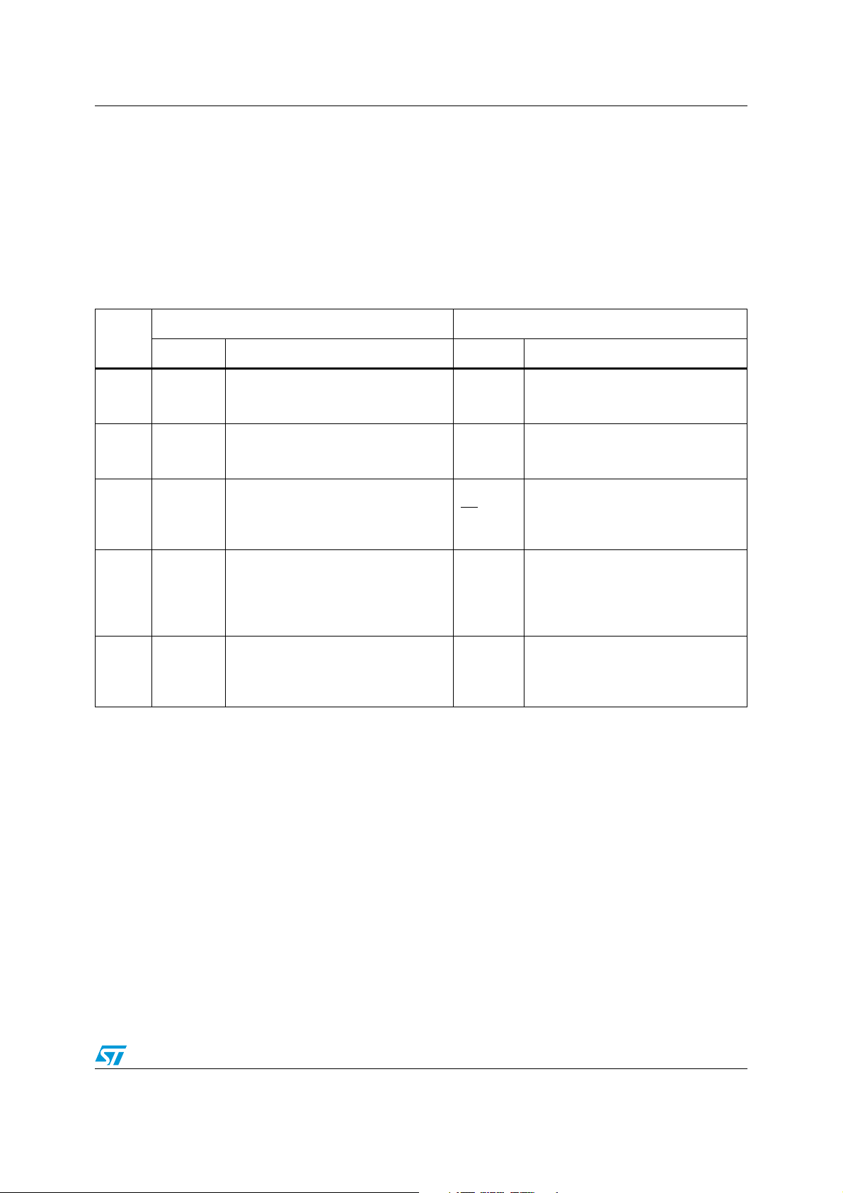
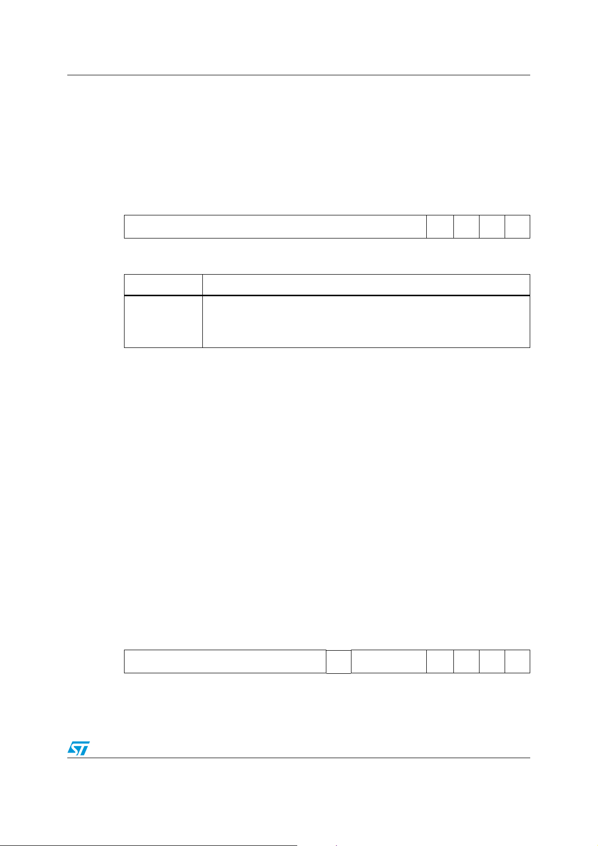
Ta bl e 1 summarizes the modifications made to the pinout.
Table 1. Pinout modifications
Pin
number
17 DC2
56 DC1
99 EA
143 V
144 V
ST10F269 ST10F272
Name Function Name Function
Internal voltage regulator decoupling.
SS
DD
Connect to nearest V
capacitor.
Internal voltage regulator decoupling.
Connect to nearest VSS via a 330nF
capacitor.
Selects code execution out of internal
Flash memory or external memory
according to level during reset.
Ground pin XTAL3
5V power supply pin XTAL4
via a 330nF
SS
V
V
EA-V
DD
18
STBY
5V power supply pin
Internal voltage regulator decoupling.
Connect to nearest V
10 - 100nF capacitor.
Selects code execution out of internal
Flash memory or external memory
according to level during reset. Power
supply input for the standby mode.
Input to the 32 kHz oscillator amplifier
circuit. When not used, must be tied to
ground to avoid consumption.
Additionally, bit OFF32 in RTCCON
register must be set.
Output of the 32 kHz oscillator
amplifier circuit. When not used, must
be left open to avoid spurious
consumption.
SS
via a
1.1.2 Pin 17
On the ST10F269, a decoupling capacitor of 330nF minimum has to be connected between
the pin 17 (named DC2) and the nearest V
This is no longer the case for the ST10F272 device where pin 17 is a V
Hardware impact
PCB must be adapted.
Software impact
None.
pin.
SS
pin.
DD
7/39
Page 8

Modified features AN2021
1.1.3 Pin 56
On the ST10F269, a decoupling capacitor of 330nF minimum has to be connected between
the pin 56 (named DC1) and the nearest V
On the ST10F272, pin 56 is named V
18
and 100nF maximum must be connected between it and the nearest V
pin.
SS
and a capacitor of value between 10nF minimum
pin.
SS
Hardware impact
Change on the capacitor value. As the value is much lower, the footprint of the capacitor
might be smaller and then a modification of the PCB is needed.
Software impact
None.
1.1.4 Pin 99
On the ST10F269, pin 99 is EA and used upon reset to select the start from the internal
Flash memory or the external memory.
On the ST10F272, pin 99 has the additional function of providing the 5V power supply to the
device in standby mode (new power-saving mode), it is called E
A-V
STBY
.
Hardware impact
The modification depends on the previous use of the ST10F269 and on whether the
Standby mode is used or not.
For an application where the Standby mode is not used, no change to the PCB is required. If
the new application uses the Standby mode, the EA
common 5V and have a specific supply path.
Software impact
None.
1.1.5 Pins 143 and 144
These pins are VSS and VDD, respectively, in the ST10F269. On the ST10F272 they are
used as XTAL3 and XTAL4 for connection to an optional 32 kHz crystal to clock the Real
Time Clock during power-down.
Hardware impact
PCB must be redesigned.
If the optional 32 kHz is not used:
● Pin 143 (XTAL3) must be linked to ground like on the ST10F269
● Pin 144 (XTAL4) must be left open. It can also be connected to ground via a capacitor
to reduce the potential RF noise that might be propagated inside the device if the pin is
left floating.
-V
pin must be separated from the
STBY
8/39
Page 9

AN2021 Modified features
Software impact
In case the optional 32 kHz is not used, the OFF32 bit of the RTCCON register must be set.
Prior to setting the OFF32 bit in the RTCCON register, the RTC must be enabled by setting
RTCEN, bit 4 of XPERCON, and XPEN, bit 2 of SYSCON.
1.2 XRAM
The ST10F272B and ST10F272E devices do not have the same size of XRAM. Each
configuration is detailed hereafter.
1.2.1 ST10F272B’s XRAM
The ST10F269 and the ST10F272B have the same size of extension XRAM: 10 Kbytes.
The XRAM of the ST10F269 is divided into two ranges being XRAM1 of 2 Kbytes and
XRAM2 of 8 Kbytes:
● The XRAM1 address range is 00’E000h - 00’E7FFh if enabled (XPEN and XRAM1EN,
bit 2 of SYSCON register and of XPERCON register, respectively, must both be set).
● The XRAM2 address range is 00’C000h - 00’DFFFh if enabled (XPEN and XRAM2EN,
bit 2 of SYSCON register and bit 3 of XPERCON register, respectively, must both be
set).
The XRAM of the ST10F272 is divided into two ranges, XRAM1 of 2 Kbytes (compatible with
the ST10F269) and XRAM2 of 8 Kbytes with a user re-programmable address range and
the StandBy mode.
● The XRAM1 address range is 00’E000h - 00’E7FFh if enabled (XPEN and XRAM1EN,
bit 2 of SYSCON register and bit 2 of XPERCON register must both be set).
● The XRAM2 address range is 09’0000h - 09’1FFFh, by default (mirrored every
16 Kbytes in the range 09’0000h -0F’FFFFh), if enabled (XPEN and XRAM2EN, bit 2 of
SYSCON register and bit 3 of XPERCON register, must both be set).
Hardware impact
None.
Software impact
There is no change in the enabling of the XRAM blocks: XPERCON register bits, XRAM1EN
and XRAM2EN, and SYSCON register bit, XPEN, are used to enable them.
The memory mapping of the application is impacted by the difference in XRAM2 location. A
new register has been created in order to allow the user to remap XRAM2 (please refer to
Section 4.1: XADRS3 register on page 28 for details).
9/39
Page 10
Modified features AN2021
1.2.2 ST10F272E’s XRAM
The ST10F269 has 10 Kbytes of extension RAM whereas the ST10F272E has 18 Kbytes.
The XRAM of the ST10F269 is divided into two ranges being XRAM1 of 2 Kbytes and
XRAM2 of 8 Kbytes:
● The XRAM1 address range is 00’E000h - 00’E7FFh if enabled.
● The XRAM2 address range is 00’C000h - 00’DFFFh if enabled.
The XRAM of the ST10F272E is divided into two ranges being XRAM1 of 2 Kbytes
(compatible with the ST10F269) and XRAM2 of 16 Kbytes with a user reprogrammable
address range:
● The XRAM1 address range is 00’E000h - 00’E7FFh if enabled (XPEN and XRAM1EN,
bit 2 of SYSCON register and bit 2 of XPERCON register, respectively, must be set).
● The XRAM2 address range is 09’0000h - 09’3FFFh, by default (mirrored every
16 Kbytes in the range 09’0000h -0F’FFFFh), if enabled (XPEN and XRAM2EN, bit 2 of
SYSCON register and bit 3 of XPERCON register, respectively, must be set).
Hardware impact
None.
Software impact
There is no change in the enabling of the XRAM blocks: XPERCON register bits, XRAM1EN
and XRAM2EN, and SYSCON register bit, XPEN, are used to enable them.
The memory mapping of the application is impacted by the difference in XRAM size and by
the location of XRAM2. A new register has been created in order to allow the user to remap
the XRAM2 (please refer to Section 4.1: XADRS3 register on page 28 for details).
1.3 Flash EEPROM
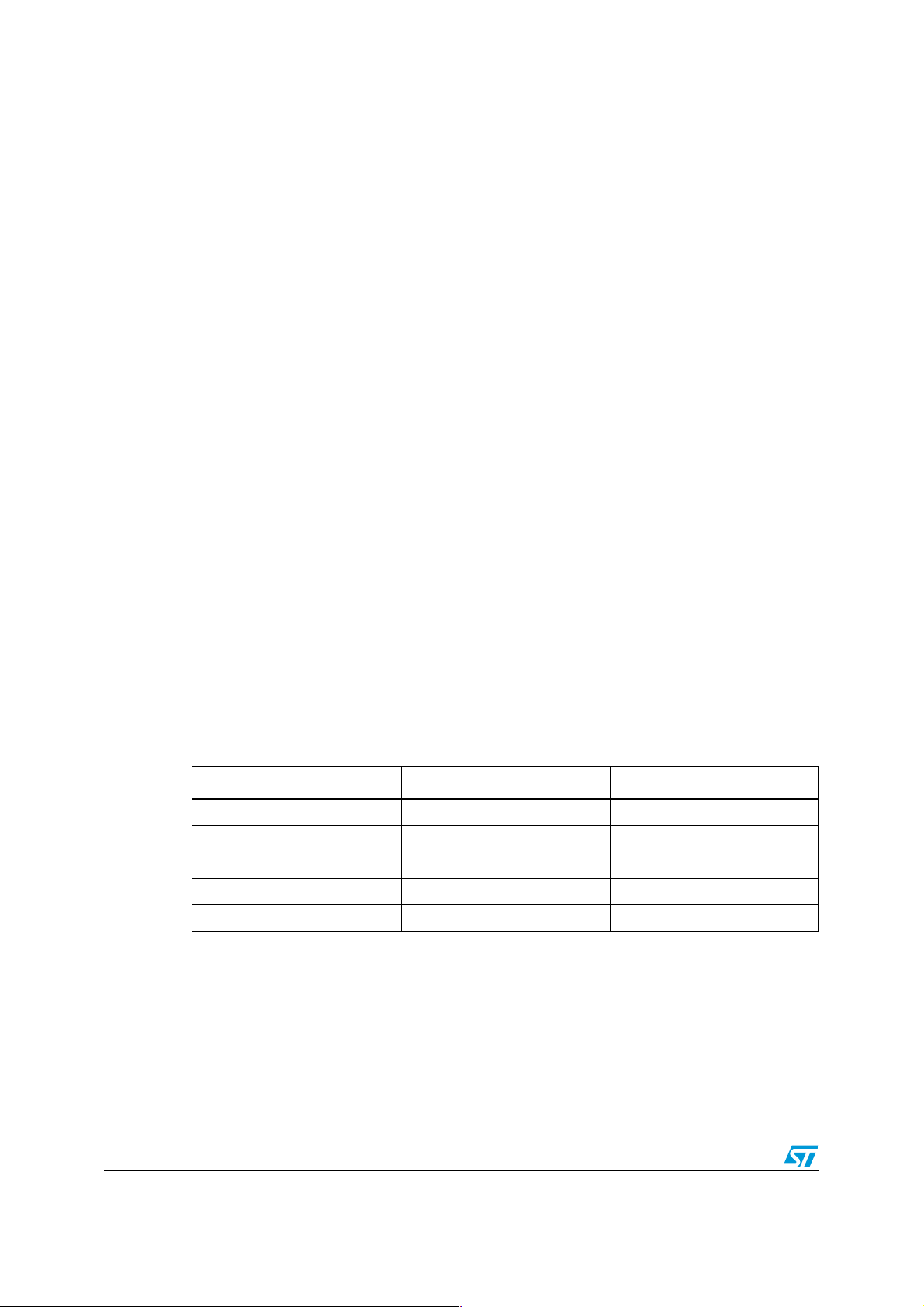
Table 2. Flash memory key characteristics
Characteristic ST10F269 ST10F272
Flash size 256 Kbytes 256 Kbytes
Flash organization 7 blocks 8 blocks
Programming voltage 5 volts 5 volts
Programming method Write/Erase Controller Write/Erase Controller
Program / Erase cycles 100000 cycles 100000 cycles
10/39
Page 11
AN2021 Modified features
Table 3. Flash memory mapping
Segment ST10F269 Flash mapping ST10F272 Flash mapping
8 08’0000-08’FFFF External memory 08’0000-08’FFFF Flash registers
7..5 05’0000-07’FFFF External memory 05’0000-07’FFFF Reserved
4 04’0000-04’FFFF Block6: 64 Kbytes 04’0000-04’FFFF Block7: 64 Kbytes
3 03’0000-03’FFFF Block5: 64 Kbytes 03’0000-03’FFFF Block6: 64 Kbytes
2 02’0000-02’FFFF Block4: 64 Kbytes 02’0000-02’FFFF Block5: 64 Kbytes
01’8000-01’FFFF Block3: 32 Kbytes 01’8000-01’FFFF Block4: 32 Kbytes
1
0
01’0000-01’7FFF
00’8000 - 00’FFFF
00’6000 - 00’7FFF Block 2: 8 Kbytes 00’6000 - 00’7FFF Block3: 8 Kbytes
00’4000 - 00’5FFF Block 1: 8 Kbytes 00’4000 - 00’5FFF Block2: 8 Kbytes
00’0000 - 00’3FFF Block 0: 16 Kbytes
External memory or
remap of Blocks 0-2
External memory
Internal RAM
and Registers
01’0000-01’7FFF
00’8000 - 00’FFFF
00’2000 - 00’3FFF Block1: 8 Kbytes
00’0000 - 00’1FFF Block0: 8 Kbytes
External memory or
remap of Blocks 0-3
External memory
Internal RAM
and Registers
1.3.1 Hardware impact
None.
1.3.2 Software impact
As the first 32 Kbytes of Flash memory are now divided into four sectors of 8 Kbytes each in
the ST10F272 whereas the ST10F269 had only three sectors, the mapping of the
application is impacted.
Moreover, the Flash memory Write/Erase controller is different and therefore the
programming routines must be updated.
When the bit ROMEN of the SYSCON register is set, that is, when the internal Flash
memory is enabled, accesses to the address range 05’0000h - 07’FFFFh are not redirected
to external memory. The linker-locator configuration of the toolchain should be checked in
order to prevent any use of this memory range.
11/39
Page 12
Modified features AN2021
1.4 A/D converter
In the ST10F272, the analog/digital converter has been redesigned (compared to the A/D
converter in the ST10F269). The ST10F272 still provides an analog/digital converter with
10-bit resolution and an on-chip sample and hold circuit.
1.4.1 Hardware / Software impact: conversion timing control
The A/D converter in the ST10F272 is not fully compatible with that of the ST10F269 (timing
and programming model).
In the ST10F269, the sample time (to charge the capacitors) and the conversion time are
programmable and can be adjusted to the external circuitry. The total conversion time is
compatible with the formula used for ST10F269, whereas the meanings of the ADCTC and
ADSTC bit fields are no longer compatible.
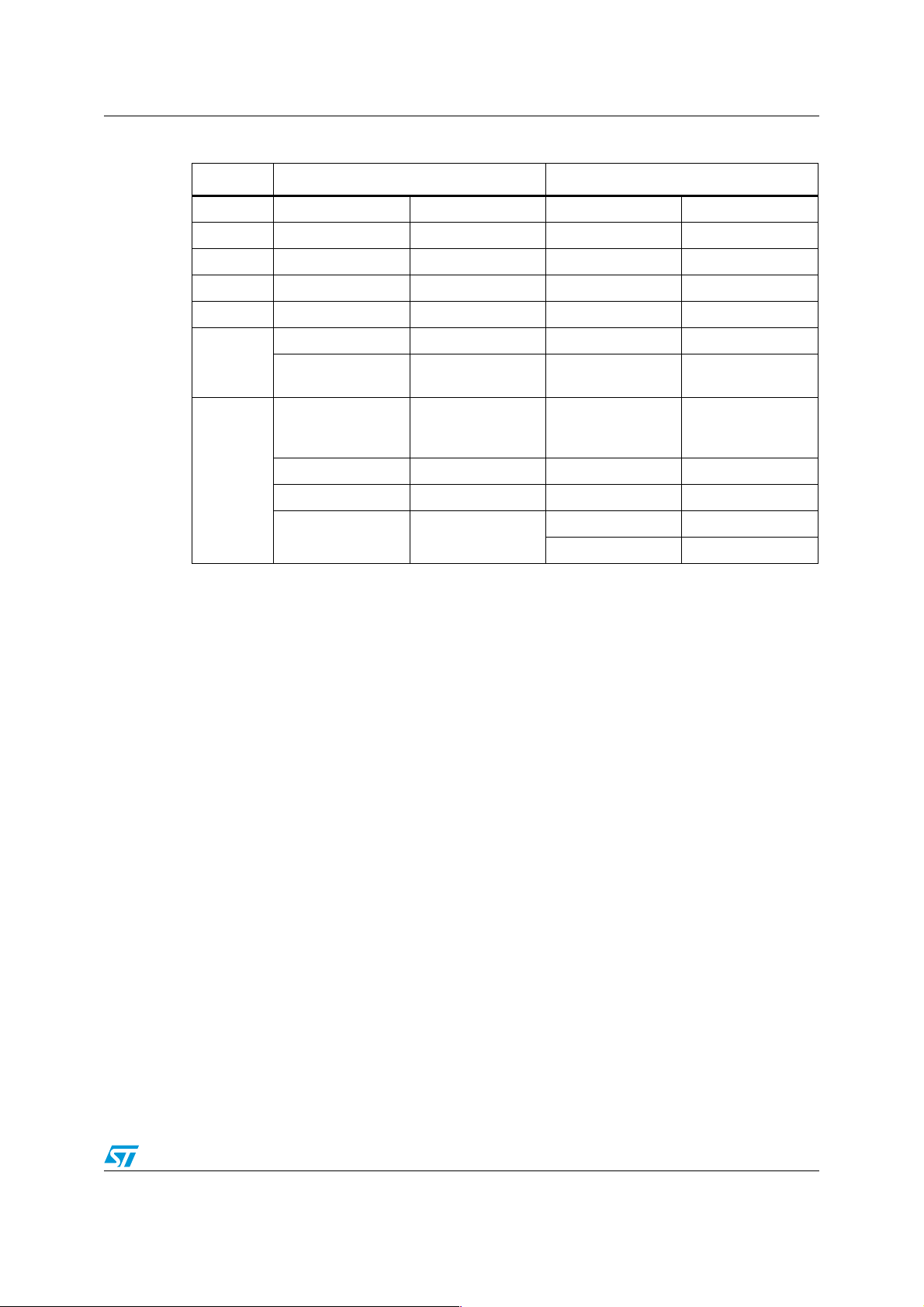
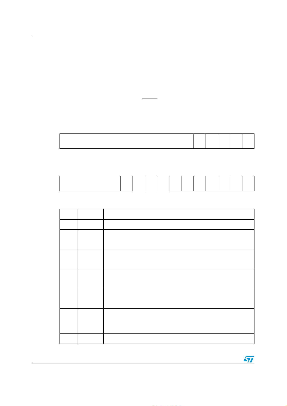
Table 4. ST10F272 conversion timing table
ADCTC ADSTC Sample Comparison Extra Total conversion
00 00 TCL * 120 TCL * 240 TCL * 28 TCL * 388
00 01 TCL * 140 TCL * 280 TCL * 16 TCL * 436
00 10 TCL * 200 TCL * 280 TCL * 52 TCL * 532
00 11 TCL * 400 TCL * 280 TCL * 44 TCL * 724
11 00 TCL * 240 TCL * 120 TCL * 52 TCL * 772
11 01 TCL * 280 TCL * 560 TCL * 28 TCL * 868
11 10 TCL * 400 TCL * 560 TCL * 100 TCL * 1060
11 11 TCL * 800 TCL * 560 TCL * 52 TCL * 1444
10 00 TCL * 480 TCL * 960 TCL * 100 TCL * 1540
10 01 TCL * 560 TCL * 1120 TCL * 52 TCL * 1732
10 10 TCL * 800 TCL * 1120 TCL * 196 TCL * 2116
10 11 TCL * 1600 TCL * 1120 TCL * 164 TCL * 2884
The user should take care of the Sample time parameter: This is the time during which the
capacitances of the converter are charged via the respective analog input pins. Ta bl e 5
shows the differences in sample time.
12/39
Page 13

AN2021 Modified features
Table 5. ST10F272 vs ST10F269 sample time comparison table
ADCTC ADSTC
ST10F269
Sample time
ST10F272
Sample time
00 00 TCL * 48 TCL * 120 2.5
00 01 TCL * 96 TCL * 140 1.46
00 10 TCL * 192 TCL * 200 1.04
00 11 TCL * 384 TCL * 400 1.04
11 00 TCL * 96 TCL * 240 2.5
11 01 TCL * 192 TCL * 280 1.46
11 10 TCL * 384 TCL * 400 1.04
11 11 TCL * 768 TCL * 800 1.04
10 00 TCL * 192 TCL * 480 2.08
10 01 TCL * 384 TCL * 560 1.46
10 10 TCL * 768 TCL * 800 1.04
10 11 TCL * 1536 TCL * 1600 1.04
In the default configuration the sample time of the ST10F272 is 2.5 times longer compared
to that of the ST10F269. This has an impact on the frequency of the input signal that can be
applied to the ST10F272.
1.4.2 Hardware impact: electrical characteristics
Ratio
F272E_time / F269_time
Ta bl e 6 lists the differences in the DC characteristics of the two devices.
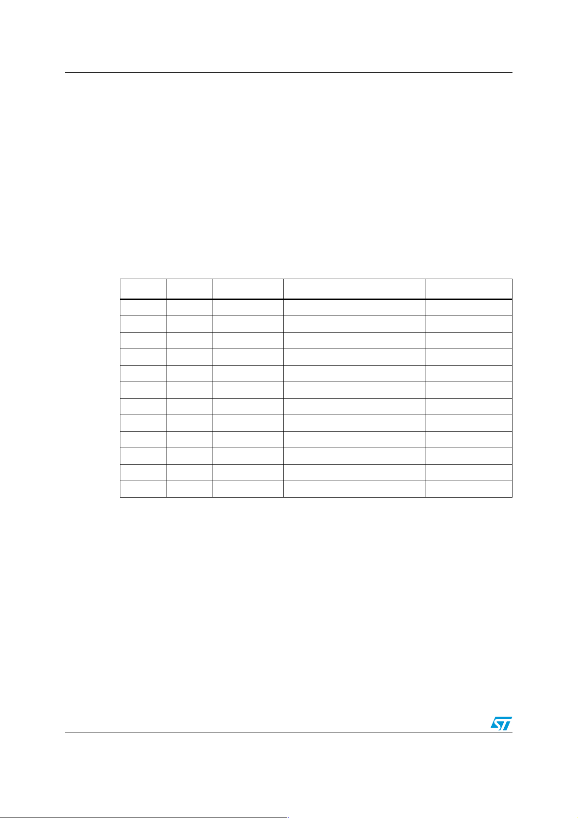
Table 6. ADC differences
Symbol Parameter
V
AREF
V
AIN
C
AIN
t
S
t
C
TUE
R
ASRC
Analog reference
voltage
Analog input voltage V
ADC input capacitance
(Port 5)
Not sampling
Sampling
Sample time 48TCL 1536TCL
Conversion time 388TCL 2884TCL 388TCL 2884TCL
Total Unadjusted Error
(Port5)
Internal resistance of
analog source
Limit values for ST10F269 Limit values for ST10F272
Min Max Min Max
4.0 V
AGND
-
-
+ 0.1 4.5 V
DD
V
AREF
V
AGND
C
10
15
-
-
1µs
120TCL
DD
V
AREF
+ CP2 +C
P1
7
10.5
1600TCL
S
-2.0 +2.0 -2.0 +2.0 LSB
[ns]/150-0.25 kΩ
t
S
Unit
V
V
pF
13/39
Page 14

Modified features AN2021
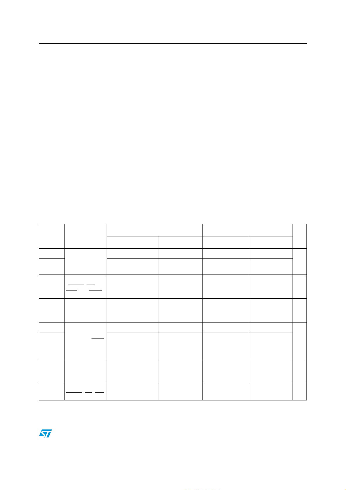
Table 6. ADC differences (continued)
Limit values for ST10F269 Limit values for ST10F272
Symbol Parameter
Min Max Min Max
Reference supply
I
AREF
current
Running mode
Power-down mode
-
-
500
1
-
-
5000
1
DNL Differential nonlinearity -0.5 +0.5 -1 +1 LSB
INL Integral nonlinearity -1.5 +1.5 -1.5 +1.5 LSB
OFS Offset error -1.0 +1.0 -1.5 +1.5 LSB
Unit
µA
µA
Note: The V
pin is also used as a supply pin for the ADC module. As there is a higher current
AREF
sink on this pin on the ST10F272 compared to the ST10F269, it is recommended not to
connect a resistor (for example, because of an RC filter), to prevent creating an offset in the
reference.
1.4.3 Software impact
Self-calibration and ADC initialization routine
An automatic self-calibration adjusts the ADC module to process parameter variations at
each reset event. After reset, the busy flag (read-only) ADBSY is set because the selfcalibration is ongoing. The duration of self-calibration depends on the CPU clock: It may
take up to 40.629 ± 1 clock pulses. The user must poll this bit to know when self-calibration
is complete in order to initialize the ADC module.
This self-calibration is seen by the ST10F272 as a conversion and thus bit ADCIR is set.
The software should perform a dummy read of the ADDAT register and clear the ADCIR and
ADCEIR flags before configuring the ADC module and starting the first conversion.
New bit ADOFF, bit 6 of ADCON register
ADCON (FFA0h / A0h) SFR Reset value: 0000h
15 14 13 12 11 10 9 8 76543210
ADCTC ADSTC
R/W R/W R/W R/W R/W RO R/W R/W R/W R/W
Table 7. ADCON register description
AD
CRQADCINADWRADBSYADSTADOFF
ADM ADCH
Bit Function Comment
ADC Disable
ADOFF
0: Analog circuitry of A/D converter is on
1: Analog circuitry of A/D converter is turned off
The bit 6 of the ADCON register, reserved in previous ST10 devices, is now used to enable
and disable the ADC. By default this bit is cleared and the ST10F272 is compatible with the
ST10F269. Therefore, there is no impact on the software, provided that this bit is not written
to.
14/39
New bit valid only for the ST10F272.
Reserved on ST10F269.
Page 15
AN2021 Modified features
Additional channels on Port1 - only for the ST10F272E
A new multiplexer selects one out of up to 16 + 8 analog input channels (alternate functions
of Port 5 and Port1). The selection of Port1 or Port5 as the input of the ADC is made via bit
ADCMUX, bit 0 of the XMISC register. By default the multiplexer selects Port5, so there is no
impact on the software as compared to an ST10F269 implementation. Note that XMISCEN,
bit 10 of the XPERCON register, must be set to have access to the XMISC register.
XMISC (EB46h) XREG Reset value: --00h
15 14 13 12 11 10 9 8 7 6 5 4 3 2 1 0
VREG
CAN
CAN
Reserved
- R/W R/W R/W R/W
Table 8. XMISC register description
Bit Function
ADC Multiplexer
ADCMUX
0: Default configuration, analog inputs on port P5.y can be converted
1: Analog inputs on port P1.z can be converted, only 8 channels can be
managed
OFF
CK2
PA R
ADC
MUX
Note: In the ST10F272B, the location of the ADCMUX bit is reserved and should not be written to,
or only to value ‘0’.
1.5 Real time clock
The RTC module can be clocked by two different sources: the main oscillator (pins XTAL1
and XTAL2) or the 32 kHz oscillator (pins XTAL3 and XTAL4). The selection of the clocking
can be made via an additional bit in the RTCCON register.
1.5.1 Hardware impact
Check the usage of pins XTAL3 and XTAL4 (pins 143 and 144, respectively).
1.5.2 Software impact
The address range of the RTC registers has been modified from 00’EC00h - 00’ECFFh on
the ST10F269, to 00’ED00h - 00’EDFFh on the ST10F272. This relocation has no impact if
the software uses register names defined by the toolchain and if the CPU selection is
changed to ST10F272. If the software was directly using the address of the RTC register, it
must be modified according to the new mapping.
ST10F269: RTCCON (F1C4h / E2h) ESFR Reset value: --00h
15 14 13 12 11 10 9 8 7 6 5 4 3 2 1 0
Reserved
- R/W - R/W R/W R/W R/W
RTC
OFF
Reserved
RTC
AEN
RTC
AIR
RTC
SEN
RTC
SIR
15/39
Page 16

Modified features AN2021
ST10F272: RTCCON (F1C4h / E2h) ESFR Reset value: 0000h
15 14 13 12 11 10 9 8 7654 3 2 1 0
RTC
RTC
RTC
OFF
Reserved
-R/WRO R/W - R/W R/W R/W R/W
Table 9. RTCCON register description
OSC
32
RTC
OFF
Reserved
AEN
AIR
SEN
RTC
SIR
Bit Function
RTC Second Interrupt Request flag (every basic clock unit)
RTCSIR
0: The bit was reset less than a Basic Clock unit ago.
1: The interrupt was triggered.
RTC Second Interrupt Enable
RTCSEN
0: RTC_SecIT is disabled.
1: RTC_SecIT is enabled; it is generated every basic clock unit.
RTC Alarm Interrupt Request flag (when the alarm is triggered)
RTCAIR
0: The bit was reset less than n Basic Clock units ago.
1: The interrupt was triggered.
RTC Alarm Interrupt Enable
RTCAEN
0: RTC_alarmIT is disabled.
1: RTC_alarmIT is enabled.
RTC Switch Off bit
0: Clock oscillator and RTC keep on running even if ST10 is in Power Down
RTCOFF
mode.
1: Clock oscillator is switched off when ST10 enters Power Down mode.
Additionally, when setting this bit, RTC dividers and counters are stopped
and registers can be written.
Reset
value
0
0
0
0
0
Oscillator Selection Flag
OSC
0: The clock oscillator used by the RTC is the main oscillator.
1: The clock oscillator used by the RTC is the low power 32 kHz oscillator.
32 kHz Oscillator Switch Off bit
0: The 32 kHz oscillator is enabled. The RTC is clocked with 32 kHz if there
OFF32
is a valid signal.
1: The 32 kHz oscillator is disabled. The RTC is clocked by the main
oscillator.
The handling of the RTCAIR and RTCSIR flags (bits 2 and 0 of the RTCCON register,
respectively) has also changed:
● In the ST10F272, these flags are cleared by writing them to ‘1’
● In the ST10F269, these flags are cleared by writing them to ‘0’
As these flags must be cleared by software when entering the corresponding interrupt
service routine, a change in the application code is needed.
16/39
0
0
Page 17

AN2021 Modified features
Example for RTCSIR flag
Replace ST10F269 code:
RTCCON &= 0xFFFE;// Clear RTCSIR flag
by the following code for ST10F272:
RTCCON |= 0x0001;// Write 1 into RTCSIR flag to clear it
1.6 CAN modules
The ST10F269 has two CAN modules of the B-CAN type.
The ST10F272 has two CAN modules of the C-CAN type. These modules are functionally
compatible with the modules of the ST10F269.
The C-CAN cells provide additional Message Objects and new functionalities. The main
difference is that the Message Objects are no longer directly accessed as memory but are
available through a Message Interface. This changes the programming model of the
modules.
1.6.1 Hardware impact
None.
1.6.2 Software impact
Rewrite the CAN drivers.
1.7 Port input control
In the ST10F269, the Port Input Control register PICON is used to select between TTL and
CMOS-like input thresholds. The CMOS-like input thresholds are defined above the TTL
levels and feature a hysteresis of 250mV to prevent the inputs from toggling while the
respective input signal level is near the thresholds. This feature is available for all pins of
Port 2, Port 3, Port4, Port 7 and Port 8.
In the ST10F272, Port 6 has been added. Moreover, the default hysteresis is now 500mV for
TTL levels and 800mV for CMOS levels.
ST10F269: PICON (F1C4h / E2h) ESFR Reset value: --00h
1514131211109876543210
Reserved
- R/W R/W - R/W R/W R/W R/W R/W
ST10F272: PICON (F1C4h / E2h) ESFR Reset value: 0000h
15 14 13 12 11 10 9 8 7 6 5 4 3 2 1 0
Reserved
- R/W R/W R/W R/W R/W R/W R/W R/W
P8
LINP7LIN
P8
LINP7LINP6LINP4LINP3HINP3LINP2HINP2LIN
P4
Res.
LINP3HINP3LINP2HINP2LIN
17/39
Page 18

Modified features AN2021
Table 10. PICON register description
Bit Function Reset value
Port x Low Byte Input Level Selection
PxLIN
PxHIN
0: Pins Px.7..0 switch on standard TTL input levels
1: Pins Px.7..0 switch on CMOS input levels
Port x High Byte Input Level Selection
0: Pins Px.15..8 switch on standard TTL input levels
1: Pins Px.15..8 switch on CMOS input levels
0
0
1.7.1 Hardware impact
None.
1.7.2 Software impact
None if the software is not writing to PICON bit 5 (P6LIN).
1.8 Ports output control
In the ST10F269, the port output control registers POCONx are used to select the output
driver characteristics of a port. In this way, the output drivers can be adapted to the
application’s requirements, and eventually, the EMI behavior of the device can be improved.
Two characteristics may be selected:
● Edge characteristic defines the rise/fall time for the respective outputs, that is, the
transition time. Slow edge reduces the peak currents that are sunk/sourced when
changing the voltage level of an external capacitive load.
● Driver characteristic defines either the general driving capability of the respective
drivers, or if the driver strength is reduced after the target output level has been
reached or not. Reducing the driver strength increases the output’s internal resistance,
which attenuates noise that is imported via the output line.
This feature is not available on the ST10F272.
1.8.1 Hardware impact
Some modifications might be needed depending on the usage of this functionality.
1.8.2 Software impact
Parts related to the initialization of the POCONx registers should be suppressed.
1.9 PLL and main on-chip oscillator
Compared to the ST10F269, several modifications have been introduced:
● PLL multiplication factors have been adapted in order to match the new frequency
range.
● On-chip main oscillator input frequency range has been reshaped, reducing it to 4 to
8 MHz: This allows the power consumption to be reduced when the Real Time Clock is
18/39
Page 19

AN2021 Modified features
running in Power Down mode and the on-chip main oscillator clock is used as the
reference.
● When the PLL is used, the CPU frequency range is 16 to 64 MHz.
Figure 1: ST10F272 clock generation diagram gives a simplified description of the CPU
clock generation. Depending on the multiplication factor selected via Port0 at reset, values
are set for each stage. The CPU clock is in fact generated mainly from a VCO with the
following characteristics:
● input range: 1 to 3.5 MHz, which explains the Prescaler that divides the XTAL
frequency
● output range: 64 to 128 MHz that is then divided through Divider1 to generate the CPU
clock
Figure 1. ST10F272 clock generation diagram
Phase Comparator
f
XTAL
Prescaler VCO Divider1
Divider2
f
CPU
Table 11: ST10F269 vs ST10F272 PLL ratio lists the new PLL multiplication factors and the
corresponding frequency ranges for the ST10F272.
Table 11. ST10F269 vs ST10F272 PLL ratio
PLL multiplication factor ST10F272 main oscillator
P0.15-13
(P0H.7-5)
ST10F269 ST10F272
Input range
(MHz)
1 1 1 x 4 x 4 4 to 8 16 to 32
1 1 0 x 3 x 3 5.34 to 8 16.02 to 24
1 0 1 x 2 x 8 4 to 8 32 to 64
1 0 0 x 5 x 5 6.4 to 8 32 to 40
0 1 1 x 1 x 1 1 to 64 1 to 64
0 1 0 x 1.5 x 10 4 to 6.4 40 to 64
0 0 1 x 0.5 x 0.5 4 to 8 2 to 4
0 0 0 x 2.5 x 16 4 64
CPU clock range
(MHz)
19/39
Page 20

Modified features AN2021
1.9.1 Hardware impact
Port0 configuration might be changed with regards to the new PLL factor.
All configurations need a crystal (or ceramic resonator) to generate the CPU clock through
the internal oscillator amplifier, except for the Direct Drive mode (oscillator amplifier
disabled, so no crystal or resonator can be used). Vice versa, the clock can be forced
through an external clock source only in Direct Drive mode.
The components on XTAL1 and XTAL2 (crystal and capacitors, or resonator) must be
changed as:
● the input frequency range is now reduced
● it is no longer possible to use a crystal or a ceramic resonator in direct drive mode
● it is no longer possible to use a PLL factor with a frequency generator
● the electrical characteristics of the main oscillator have changed (transconductance)
1.9.2 Software impact
None.
20/39
Page 21

AN2021 New features
2 New features
2.1 Additional XPeripherals
Some peripherals have been added to the ST10F272. They are mapped on the XBus and
are linked to additional alternate functions of some ports of the ST10F272.
The additional XPeripherals are the following:
● A second SSC (SSC of ST10F269 becomes SSC0, while the new one is referred to as
XSSC or simply SSC1). Note that some restrictions and functional differences due to
the XBus peculiarities are present between the standard SSC, and the new XSSC.
● A second ASC (ASC0 of ST10F269 remains ASC0, while the new one is referred to as
XASC or simply as ASC1). Note that some restrictions and functional differences due
to the XBus peculiarities are present between the standard ASC, and the new XASC.
● An I2C interface is added (see X-I2C or simply I2C interface).
In addition to the previous XPeripherals, the ST10F272E also features a second PWM
(PWM of ST10F269 becomes PWM0, while the new one is referred to as XPWM or simply
as PWM1). Note that some restrictions and functional differences due to the XBus
peculiarities are present between the standard PWM, and the new XPWM.
2.1.1 Hardware impact
None if the additional XPeripherals are not used.
2.1.2 Software impact
None if the additional Peripherals are not used. As they are XPeripherals, they can be
enabled / disabled via the XPERCON and SYSCON registers. By default, the settings of
XPERCON and SYSCON are compatible with the ST10F269.
2.2 Programmable divider on CLKOUT
A specific register mapped on the XBus is used to choose the division factor on the
CLKOUT signal (P3.15).
XCLKOUTDIV (E902h) XBUS Reset value: --00h
15 14 13 12 11 10 9 8 7 6 5 4 3 2 1 0
Reserved DIV
-R/W
Table 12. XCLKOUTDIV register description
Bit Function
DIV f
clkout
= f
CPU
/ (DIV + 1)
21/39
Page 22

New features AN2021
2.2.1 Hardware impact
None.
2.2.2 Software impact
None if only CLKOUT is needed.
When the CLKOUT function is enabled by setting the CLKEN bit in the SYSCON register, by
default the CPU clock is output on P3.15.
To have access to the XCLKOUTDIV register, and thus to program the clock pre-scaling
factor, the XMISCEN bit in the XPERCON register and the XPEN bit in the SYSCON
register must be set.
2.3 New multiplexer for X-Interrupts
The limited number of XBus interrupt lines of the present ST10 architecture imposes some
constraints on the implementation of the new functionalities. In particular, the additional
XPeripherals XSSC, XASC, XI2C and XPWM need some resources to implement interrupt
and PEC transfer. For this reason, a complex but very flexible multiplexed structure for the
interrupt is proposed. In Figure 2, the principle is represented through a simple diagram,
which shows the basic structure replicated for each of the four X-interrupt vectors (XP0INT,
XP1INT, XP2INT and XP3INT).
It is based on a new 16-bit register XIRxSEL (x = 0,1,2,3), divided into 2 bytes:
● Higher Byte (XIRxSEL[15:8]) Interrupt Enable bits
● Lower Byte (XIRxSEL[7:0]) Interrupt Flag bits
Figure 2. X-Interrupt basic structure
70
Flag[7:0]
IT Source 7
IT Source 6
IT Source 5
IT Source 4
IT Source 3
IT Source 2
IT Source 1
IT Source 0
Enable[7:0]
15 8
XIRxSEL[7:0] (x = 0, 1, 2, 3)
XPxIC.IR (x = 0, 1, 2, 3)
XIRxSEL[15:8] (x = 0, 1, 2, 3)
When different sources submit an interrupt request, the enable bits (Byte High of XIRxSEL
register) define a mask which controls which sources will be associated with the unique
available vector. If more than one source is enabled to issue the request, the service routine
has to identify the real event to be serviced. This can easily be done by checking the flag
22/39
Page 23

AN2021 New features
bits (Byte Low of XIRxSEL register). Note that the flag bit can provide information about
events which are not currently serviced by the interrupt controller (since masked through the
enable bits), allowing an effective software management also in the absence of the
possibility to serve the related interrupt request: a periodic polling of the flag bits may be
implemented inside the user application.
Table 13: X-Interrupt detailed mapping gives an overview of the different settings available.
Table 13. X-Interrupt detailed mapping
XP0INT XP1INT XP2INT XP3INT
CAN1 Interrupt X X
CAN2 Interrupt X X
I2C Receive X X X
I2C Transmit X X X
I2C Error X
SSC1 Receive X X X
SSC1 Transmit X X X
SSC1 Error X
ASC1 Receive X X X
ASC1 Transmit X X X
ASC1 Transmit Buffer X X X
ASC1 Error X
PLL Unlock / OWD X
PWM1 Channel 3...0 X X
2.3.1 Hardware impact
None.
2.3.2 Software impact
First, the XMISCEN bit, that is, bit 10 of the XPERCON register, must be set to have access
to these registers. Refer to Section 3.1: XPERCON register for more details.
Then, the XIRxSEL registers must be configured. If none of the new XPeripherals is used,
that is, only the XPeripherals that were already present on the ST10F269 are used, the
following values must be programmed:
● XIR0SEL = 0x0100, only the CAN1 interrupt is enabled and can generate an interrupt
to the ST10 through XP0IC
● XIR1SEL = 0x0100, only the CAN2 interrupt is enabled and can generate an interrupt
to the ST10 through XP1IC
● XIR2SEL = 0x0, not used
● XIR3SEL = 0x2000, only the PLL unlock interrupt is enabled and can generate an
interrupt to the ST10 through XP3IC
23/39
Page 24

New features AN2021
Then, in the interrupt routines associated with the XPxIC, the respective flags in the
XIRxSEL registers must be cleared. Since the XIRxSEL registers are not bit addressable, a
pair of registers (a pair for each XIRxSEL) is provided to set and clear the bits of XIRxSEL
without risking to overwrite requests coming after reading the register and before writing it.
Therefore, the following registers must be written to clear the flags:
● in the CAN1 interrupt routine, XIR0CLR (@ EB14h) = 0x0001
● in the CAN2 interrupt routine, XIR1CLR (@ EB24h) = 0x0001
● in the PLL unlock interrupt routine, XIR3CLR (@ EB44h) = 0x0020
Additional information on the X-Interrupt multiplexer structure
Figure 2: X-Interrupt basic structure shows that the X-Interrupt sources are connected to the
interrupt request flag of the XIRxSEL registers and to the XPxIR request flag via an AND
gate with the enable bit. This AND gate is activated by a transition on the Interrupt source
line and not by the latched value in the XIRxSEL register. This means that:
● A transition on the IT source line generates an interrupt to the ST10 core if the source
is enabled.
● Writing to an interrupt request flag in an XIRxSEL register does not generate an
interrupt to the ST10 core.
Example:
If XIR0SEL = 0x0100: CAN1 interrupt enabled on XP0IC interrupt
To trigger by software the CAN1 interrupt routine with the XP0IC register, the following code
must be used:
XIR0SET = 0x0001;/* Set CAN1 interrupt request Flag in XIR0SEL */
XP0IC = XP0IC | 0x0080;/* Set XP0IR flag, generate an interrupt */
Executing only the first line only sets the flag in the XIR0SEL register but it is not seen by the
AND gate and cannot set the XP0IR flag.
24/39
Page 25

AN2021 New features
2.4 Additional ports input control
The possibility to select between TTL and CMOS-like input thresholds has been extended to
Ports 0, 1 and 5 via the XPICON register.
ST10F272: XPICON (EB26h) XREG Reset value: --00h
15 14 13 12 11 10 9 8 7 6 5 4 3 2 1 0
Reserved
- R/W R/W R/W R/W R/W R/W
Table 14. XPICON register description
Bit Function Reset value
Port x Low Byte Input Level Selection
PxLIN
0: Pins Px.7..0 switch on standard TTL input levels
1: Pins Px.7..0 switch on CMOS input levels
Port x High Byte Input Level Selection
PxHIN
0: Pins Px.15..8 switch on standard TTL input levels
1: Pins Px.15..8 switch on CMOS input levels
P5
HINP5LINP1HINP1LINP0HINP0LIN
0
0
2.4.1 Hardware impact
None.
2.4.2 Software impact
None.
25/39
Page 26
Modified registers AN2021
3 Modified registers
3.1 XPERCON register
In the ST10F272, new bits have been added with regards to the additional XPeripherals.
The XPERCON register allows the XBus peripherals to be separately selected and made
visible to the user by means of the corresponding bits. If an XBus peripheral is not selected
(not activated with a bit of XPERCON) before
corresponding address space, port pins and interrupts are not occupied by the peripheral,
and thus this peripheral is not visible and not available.
ST10F269: XPERCON (F024h / 12h) SFR Reset value: --05h
1514131211109876543210
the XPEN bit in SYSCON is set, the
Res.
RTC
EN
RTC
EN
EN
XRAM2
XRAM2ENXRAM1
Reserved
- R/W R/W R/W R/W R/W
ST10F272: XPERCON (F024h / 12h) SFR Reset value: -005h
1514131211109876543210
Reserved
- R/W R/W R/W R/W R/W - R/W R/W R/W R/W R/W
Table 15. XPERCON register description
XI2CENXSSCENXASC
EN
XMISC
EN
EN
XPWM
CAN2ENCAN1
EN
XRAM1
CAN2ENCAN1
EN
EN
EN
Bit Bit name Function
15:11 - Reserved
XBUS Additional Features Enable Bit
10 XMISCEN
0: Accesses to the Additional Miscellaneous Features is disabled.
1: The Additional Features are enabled and can be accessed.
XI 2 C Enable Bit
9XI2CEN
0: Accesses to the on-chip XI 2 C are disabled, external access performed.
1: The on-chip XI 2 C is enabled and can be accessed.
XSSC Enable Bit
8 XSSCEN
0: Accesses to the on-chip XSSC are disabled, external access performed.
1: The on-chip XSSC is enabled and can be accessed.
XASC Enable Bit
7 XASCEN
0: Accesses to the on-chip XASC are disabled, external access performed.
1: The on-chip XASC is enabled and can be accessed.
XPWM Enable
6XPWMEN
0: Accesses to the on-chip XPWM module are disabled, external access
performed.
1: The on-chip XPWM module is enabled and can be accessed.
5-Reserved
26/39
Page 27

AN2021 Modified registers
Table 15. XPERCON register description (continued)
Bit Bit name Function
RTC Enable Bit
4RTCEN
3XRAM2EN
2XRAM1EN
1CAN2EN
0CAN1EN
0: Accesses to the on-chip Real Time Clock are disabled, external access
performed.
1: The on-chip Real Time Clock is enabled and can be accessed.
XRAM2 Enable Bit
0: Accesses to the on-chip XRAM2 block are disabled, external access
performed.
1: The on-chip XRAM2 is enabled and can be accessed.
XRAM1 Enable Bit
0: Accesses to the on-chip XRAM1 block are disabled, external access
performed.
1: The on-chip XRAM1 is enabled and can be accessed.
CAN2 Enable Bit
0: Accesses to the CAN2 XPeripheral and its functions are disabled (P4.4
and P4.7 pins can be used as general purpose I/Os)
1: The CAN2 XPeripheral is enabled and can be accessed.
CAN1 Enable Bit
0: Accesses to the CAN1 XPeripheral and its functions are disabled (P4.5
and P4.6 pins can be used as general purpose I/Os)
1: The CAN1 XPeripheral is enabled and can be accessed.
Accesses to the XPeripherals are configured through three pairs of specific XBus
configuration registers, equivalent to the External Bus register BUSCONx and ADDRSELx.
Therefore, several XPeripherals are sharing the same pair, with the consequence that
accesses to a disabled XPeripherals are only redirected to external memory if all the other
XPeripherals sharing the same pair of registers are disabled.
The XPeripherals are grouped as follows:
● CAN1, CAN2, XASC, XSSC, XI2C, XPWM, XRTC and XMISC: Accesses to the
00’E800h-00’EFFFh range are redirected to external memory only if all corresponding
bits are cleared
● XRAM1: Accesses to the 00’E000h-00’E7FFh range are redirected to external memory
if bit XRAM1EN is cleared
● XRAM2: Accesses the 09’0000h-0F’FFFFh range (default value in XADRS3 register,
refer to Section 4.1: XADRS3 register) are redirected to external memory if bit
XRAM2EN is cleared
3.1.1 Hardware impact
None.
3.1.2 Software impact
None if the ST10F269 software is not writing to the reserved bit.
27/39
Page 28

New registers AN2021
4 New registers
4.1 XADRS3 register
On previous ST10 devices, this register was already present but its value was mask
programmed. On the ST10F272 this register has been made available to the user. In this
way the address range of the XRAM2 memory is now user-programmable.
ST10F272: XADRS3 (F01Ch) SFR Reset value: 800Bh
1514131211109876543210
RGSAD RGSZ
R/W R/W
The register functionality is the same as that of ADDRSELx registers used for external
address range selection, with some limitations:
● The address window can only be located in the first megabyte of addressable space,
that is, in the 00’0000h-0F’FFFFh range
● The window start address must be aligned to a Range Size boundary
Table 16. XADRS3 register description
Bit Bit name Function
15:4 RGSAD
3:0 RGSZ
Table 17. Definition of address area
Bit field
RGSZ
Selected window
size
0 0 0 0 256 bytes RRRR RRRR RRRR 0000 RRRR RRRR RRRR xxxx xxxx
0 0 0 1 512 bytes RRRR RRRR RRRx 0000 RRRR RRRR RRRx xxxx xxxx
... ... ... ...
1 0 1 0 256 Kbytes RRxx xxxx xxxx 0000 RRxx xxxx xxxx xxxx xxxx
1 0 1 1 512 Kbytes Rxxx xxxx xxxx 0000 Rxxx xxxx xxxx xxxx xxxx
1 1 x x Reserved
4.1.1 Hardware impact
None.
Range Start Address
Defines the bits A19..A8 of the start address of the address window.
Range Size Selection
Defines the size of the address window.
Relevant bit (R) of
RGSAD
Selected range Start Address
Relevant bit (R) of Address (A23 - A0)
28/39
Page 29

AN2021 New registers
4.1.2 Software impact for the ST10F272B
On ST10F272B, this register must be programmed by the user before accessing XRAM2 so
that:
● RGSZ defines an 8 Kbyte window size. RGSZ = 0101b
● RGSAD defines bits 8 to 19 of the window start address aligned to an 8 Kbyte
boundary (the least significant bits of the field are not relevant).
By programming XADRS3 to 0C05h, the XRAM2 will be 8 Kbytes, mapped from 00’C000h
to 00’DFFFh, exactly as in the ST10F269.
Note: XADRS3 cannot be changed after executing the EINIT instruction.
4.1.3 Software impact for the ST10F272E
On ST10F272E, this register must be programmed by the user before accessing XRAM2 so
that:
● RGSZ defines a 16 Kbyte window size. RGSZ = 0110b
● RGSAD defines bits 8 to 19 of the window start address aligned to a 16-Kbyte
boundary (the least significant bits of the field are not relevant).
In the ST10F272E, the XRAM2 cannot be located within page 3 of segment 0. The user can
either:
● map the XRAM2 from anywhere above address 09’0000h
● map the XRAM2 in the 16-Kbyte page available in segment 0 in the 00’8000h -
00’BFFFh range.
The desired value should be written in XADRS3 register before enabling XRAM2 in the
SYSCON and XPERCON registers.
Note: XADRS3 cannot be changed after executing the EINIT instruction.
Example
To map the 16-Kbyte XRAM2 onto page 60 (starting address 0F’0000h, compatible
with the ST10F276E), then XADRS3 must be initialized with the value F006h.
To map the 16-Kbyte XRAM2 onto page 2 (starting address 00’8000h), then XADRS3
must be initialized with the value 0806h.
Variables and PEC transfers
For architecture reasons, the PEC destination and source pointers must be in the segment
0. Therefore, all RAM variables and arrays that are PEC-addressed must be located in RAM
memory available in segment 0 (DPRAM + XRAM1, and XRAM2 if remapped onto page 2).
About Toolchain memory model
A change in the Toolchain configuration is needed to take into account the XRAM2’s new
location. In the ST10F269, all the XRAM is in page 3 and it is then automatically addressed
using DPP3 that points to page 3 (in order to access the DPRAM and the SFR/ESFR). For
the ST10F272, it is necessary to dedicate a DPP to access some of XRAM2.
29/39
Page 30

New registers AN2021
Example in case of Small memory model with tasking toolchain
The Small memory model makes it possible to have a total code size up to 16 Mbytes, up to
64 Kbytes of fast accessible 'normal user data' in three different memory configurations and
the possibility to access far/huge data, if more than 64 Kbytes of data is needed.
The three memory configurations possible for this 64 Kbytes of 'normal user data' are:
● Default
The four DPP registers are assumed to contain their system startup value (0-3),
providing one linear data area of 64 Kbytes in the first segment (00’0000h - 00’FFFFh).
● Addresses Linear
DPP3 contains page number 3, allowing access to SYSTEM (extended) SFR registers
and bit-addressable memory. DPP0 - DPP2 provide a linear data area of 48 Kbytes
anywhere in memory.
● Paged
DPP3 contains page number 3, allowing access to SYSTEM (extended) SFR registers
and bit-addressable memory. DPP0, DPP1 and DPP2 contain the page number of a
data area of 16 Kbytes anywhere in memory.
Therefore, mapping the XRAM2 onto page 2 (segment 0) makes it available for PEC transfer
and the default configuration of the C compiler toolchains can still be used.
4.2 XPEREMU register
This register has been added as a write-only register.
ST10F272: XPEREMU (EB7Eh) XREG Reset value: XXXXh
1514131211109876543210
Reserved
- WOWOWOWOWO - WOWOWOWOWO
The bit meaning is exactly the same as in the XPERCON register.
4.2.1 Hardware impact
None.
4.2.2 Software impact
Once the XPEN bit of the SYSCON register is set and at least one of the XPeripherals
(except for memories) is activated, the XPEREMU register must be written with the same
contents as the XPERCON register: This is mandatory in order to allow a correct emulation
of the new set of features introduced on XBus for the new ST10 generation. The following
instructions must be added inside the initialization routine:
XMIS
CEN
XI2
CEN
XSS
CEN
XAS
CEN
XPW
MEN
Res.
XRT
CEN
XRAM2ENXRAM1
EN
CAN2ENCAN1
EN
if (SYSCON.XPEN && (XPERCON & 0x07D3))
then {XPEREMU = XPERCON}
30/39
Page 31

AN2021 New registers
Of course, XPEREMU must be programmed after XPERCON and after SYSCON. In this
way, the final configuration for XPeripherals is stored in XPEREMU and used for the
emulation hardware setup.
4.3 Emulation-dedicated registers
A set of four additional registers is implemented for emulation purposes only. Similarly to the
XPEREMU, they are write-only registers.
XEMU0 (00’EB76h)
XEMU1 (00’EB78h)
XEMU2 (00’EB7Ah)
XEMU3 (00’EB7Ch)
These registers are used by emulators. They have no user action on the ST10F272.
4.3.1 Hardware impact
None.
4.3.2 Software impact
None. On the ST10F269, the 00’E800h to 00’EBFFh address range was mapped to external
memory but is recommended to reserve this space for upward compatibility.
4.4 XMISC register
This register has been created to handle some additional functionalities. To have access to
this register, the XMISCEN bit, that is, bit 10 of XPERCON, must be set.
ST10F272: XMISC (EB46h) XREG Reset value: 0000h
151413121110987654 3 210
Table 18. XMISC register description
Bit Bit name Function
15:4 - Reserved
3VREGOFF
2 CANCK2
VREG
CAN
Reserved
- R/W R/W R/W R/W
OFF
CK2
CAN
PA R
Main Voltage Regulator disable in Power-Down mode
0: Default value after reset and when Power-Down is not used
1: On-chip Main Regulator is turned off when Power-Down mode is entered
CAN Clock divider by 2 disable
0: Clock provided to CAN modules is CPU clock divided by 2 (mandatory
when f
is higher than 40 MHz)
CPU
1: Clock provided to CAN modules is directly CPU clock
ADC
MUX
31/39
Page 32

New registers AN2021
Table 18. XMISC register description (continued)
Bit Bit name Function
CAN Parallel Mode Selection
0: CAN2 is mapped on P4.4/P4.7, while CAN1 is mapped on P4.5/P4.6
1CANPAR
0 ADCMUX
1: CAN1 and CAN2 are mapped in parallel on P4.5/P4.6. This is effective
only if both CAN1 and CAN2 are enabled (bits CAN1EN and CAN2EN set
in XPERCON register). If CAN1 is disabled, CAN2 remains on P4.4/P4.7
even if the CANPAR bit is set.
Port1L ADC Channels Enable
0: Analog inputs on port P5.y can be converted (default configuration)
1: Analog inputs on port P1.z can be converted. Only 8 channels can be
managed
4.4.1 Hardware impact
None.
4.4.2 Software impact
None.
32/39
Page 33
AN2021 Electrical characteristics
5 Electrical characteristics
Note: In the tables where the device provides signals with their respective timing characteristics,
the symbol CC (Controller Characteristics) is included in the Symbol column.
In the tables where the external system must provide signals with their respective timing
characteristics to the device, the symbol SR (System Requirement) is included in the
Symbol column.
5.1 DC characteristics
5.1.1 Absolute maximum ratings
They are the same.
5.1.2 Overview of the DC characteristics
The pads of the ST10F272 have been redesigned according to the new technology and
therefore the characteristics are different. The user should verify the DC characteristics.
Ta bl e 1 9 lists the parameters that might be impacted most.
Table 19. DC characteristics
Symbol Parameter
VILSR
-0.5 0.2 VDD - 0.1 -0.3 0.8
Input low voltage
V
ILS
(all inputs)
SR -0.5
Input low voltage
SR
V
IL1
(RSTIN
and RPD)
NMI,
, EA,
N.A. N.A. -0.3 0.3 V
Input low voltage
V
SR
IL2
(XTAL1 and
XTAL3)
SR Input high
V
IH
0.2 V
voltage
V
IHS
(all except RPD,
SR 0.8 VDD - 0.2
XTAL1 and
XTAL3)
HYSCC
Input Hysteresis
N.A.
400, special
threshold
Input Hysteresis
CC
V
HYS1
RSTIN, EA, NMI
ST10F269 Limit values ST10F272 Limit values
Min Max Min Max
2.0, special
threshold
-0.3
0.3 V
threshold
-0.3 0.3 V
+ 0.9 VDD + 0.5 2.0 VDD + 0.3
DD
V
+ 0.5,
DD
special threshold
0.7 V
DD
- 400, default
750, special
VDD + 0.3,
special threshold
700
1400
threshold
750 1400 mV
, special
DD
DD
DD
Unit
V
V
V
V
mV
33/39
Page 34

Electrical characteristics AN2021
Table 19. DC characteristics (continued)
ST10F269 Limit values ST10F272 Limit values
Symbol Parameter
Min Max Min Max
Unit
VOLCC
V
CC
OL1
CC
V
OH
V
CC
OH1
I
CC
OZ1
CC
I
OZ2
Output low
voltage
Output low
voltage (all
other)
Output high
voltage
Output high
voltage (all
other)
Input leakage
current (Port 5)
Input leakage
current (all other
inputs)
–
Port0, Port1, Port4,
ALE, RD
, WR, BHE,
CLKOUT, RSTOUT
0.45 / IOL =
2.4mA
–
Port6, ALE,
CLKOUT, WR
READY, BHE
,
, RD,
0.4 / IOL = 8mA
0.05 / I
= 1mA
OL
V
RSTOUT, RSTIN
–0.45/I
OL
=
2.4mA
0.9V
DD/IOH
-0.5mA
2.4 / I
= -2.4mA
OH
=
–
Por t 0, Por t1,
Por t 4, RD, ALE,
, WR,
BHE
CLKOUT,
RSTOUT
= -1.6mA
OH
=
–
0.9V
DD/IOH
-0.25mA
2.4 / I
–0.4/I
0.05 /
I
VDD - 0.8 / IOH =
-8mA
- 0.08/ IOH =
V
DD
-1mA
–
Port6, ALE,
CLKOUT, WR
READY, BHE
=0.5mA
OL
=4mA
OL
V
,
V
,
RD, RSTOUT,
RSTIN
- 0.8 / IOH =
V
DD
-4mA
-0.08/IOH =
V
DD
–V
-0.5mA
– ±0.5 – ±0.2 µA
–±1–±0.5µA
5.2 AC characteristics at 40 MHz
As the two devices have a different technology, the I/Os also present some differences in the
AC behavior. The tables below (Tab le 2 0 and Ta bl e 2 1) list all the timing differences. Please
check carefully your design for possible impact.
5.2.1 External memory bus timings
Note that for CPU clock frequencies above 40 MHz, some numbers in the timing formulas
become zero or negative, that in most of the cases is not acceptable or not meaningful at all.
In these cases, it is necessary to reduce the speed of the bus setting properly t
extension), t
34/39
(Memory Cycle Time wait-states) and tF (Memory tri-state time).
C
(ALE
A
Page 35
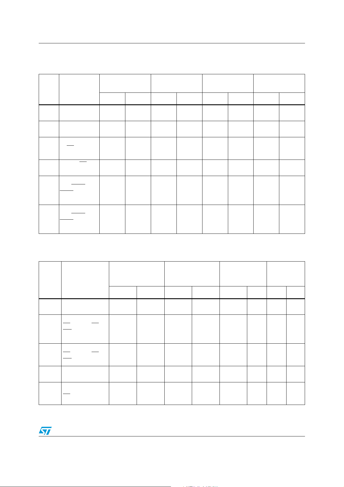
AN2021 Electrical characteristics
Multiplexed bus
Table 20. Multiplexed bus timings (ns)
ST10F269 ST10F272
Symbol Parameter
Min Max Min Max Min Max Min Max
t
CC
6
t
SR
16
t17SR
t39SR
Address setup to
ALE
ALE low to valid
data in
Address/Unlatch
ed CS to valid
data in
Latched CS
to valid data In
low
TCL - 10.5
+ t
A
-
-
-
-
3 TCL - 19
+ t
+ t
A
4 TCL - 28
+ t
+ 2t
A
3 TCL - 19
+ 2tA + t
Address float
t44CC
after RdCS
WrCS (with RW
,
-0-1.5-0-1.5
delay)
Address float
45
WrCS
after RdCS
CC
t
,
(no RW
- TCL - TCL + 1.5 - 12.5 - 14
delay)
Demultiplexed bus
Table 21. Demultiplexed bus timings
TCL - 11 +
C
C
C
t
A
-
-
-
ST10F269
= 40 MHz
@f
CPU
-2 + tA- 1.5 + t
+ t
A
A
A
C
+ t
+ t
18.5 + tA +
22 + 2tA +
C
18.5 + 2tA
+ t
C
t
C
t
C
C
-
-
-
3 TCL - 20
+ t
4 TCL - 30
+ 2t
3 TCL - 21
+ 2t
ST10F272
@f
CPU
17.5 + t
t
C
20 + 2t
t
C
16.5 + 2t
+ t
C
= 40 MHz
A
+
A
+
A
A
-
-
-
-
Symbol Parameter
6
ALE
Address setup to
CC
t
Address/Unlatched
CC
CS
(with RW
WR
t
80
setup to RD,
delay)
Address/Unlatched
t81CC
t
16
t17SR
CS setup to RD,
(no RW delay)
WR
ALE low to valid
SR
data in
Address/Unlatched
to valid data in
CS
ST10F272
@f
CPU
40 MHz
ST10F269 ST10F272
ST10F269
@f
CPU
= 40 MHz
Min Max Min Max Min Max Min Max
TCL -
10.5 + t
-
-
-
-
A
8.5 + 2t
TCL - 8.5
3 TCL - 19
4 TCL - 28
+ 2t
-
2 TCL -
+ 2t
+ t
+ t
A
A
A
+ t
A
C
C
TCL - 11
+ t
A
-
-
-
-
-2 + tA-
2 TCL -
12.5 + 2t
TCL - 12
+ 2t
3 TCL - 20
+ t
A
4 TCL - 30
+ 2t
A
+ t
+ t
A
A
C
C
16.5 + 2t
4 + 2t
18.5 + tA
+ t
22 + 2tA +
1.5 +
t
A
12.5 +
-
A
A
C
2t
A
0.5 +
2t
A
17.5 +
+ t
t
A
C
20 +
-
t
C
2tA +
t
C
35/39
=
-
-
-
-
-
Page 36

Electrical characteristics AN2021
Table 21. Demultiplexed bus timings (continued)
ST10F269 ST10F272
Symbol Parameter
Min Max Min Max Min Max Min Max
Address/Unlatched
t28CC
CS hold after RD,
WR
t39SR
Latched CS
valid data in
CC Address setup to
t
82
RdCS
, WrCS (with
RW delay)
low to
0 (no tF)
-5 + t
(tF > 0)
-
2 TCL -
10.5 + 2t
F
A
-0 + t
3 TCL - 19
+ 2tA + t
-
C
2 TCL - 11
+ 2t
-
F
A
-
3 TCL - 21
+ t
+ 2t
A
- 14.5 + 2t
5.2.2 Hi-speed synchronous serial interface (SSC)
The maximum baudrate of the SSC in the ST10F272 is 8 Mbaud whereas it is 10 Mbaud in
the ST10F269. For CPU frequencies strictly higher than 32 MHz, the minimum value in the
SSCBR register (prescaler value) must not be lower than 2.
@f
0 (no t
18.5 + 2tA
C
ST10F269
CPU
F
-5 + t
F
(tF > 0)
+ t
C
= 40 MHz
)
-0 + t
-
-
A
ST10F272
@f
CPU
40 MHz
F
16.5 +
2tA +
t
C
14 +
2t
A
=
-
-
-
36/39
Page 37

AN2021 Referenced documents
6 Referenced documents
The following documents were used to write this application note:
● ST10F269 datasheet, 16-BIT MCU WITH MAC UNIT, 256K BYTE FLASH MEMORY
AND 12K BYTE RAM, revision of March 2003
● ST10F272B-E Final Data, 16-bit MCU with 256 Kbyte Flash memory and 12/20 Kbyte
RAM, Rev. 1, 20 July 2006
37/39
Page 38

Revision history AN2021
7 Revision history
Table 22. Revision history
Date Revision Changes
First Issue with the 2 devices in the same document
November 2004 1
24-Jan-2007 2
Previously 2 separate documents for ST10F272B and
ST10F272E (last version December 2003)
Converted to new ST template
Chapter on page 1: Minor editing changes
Changed presentation of registers throughout document
Section 1.4.3: Software impact: Changed name of bit 11 from
ADCTC to ADCRQ
Table 8 on page 15: Added bit name ADC Multiplexer to
function field of bit ADCMUX
Table 9 on page 16: Changed OSC reset value from “U” to “0”
Section 1.7: Port input control: Replaced ST10F276 with
ST10F272 in register name
Section 1.9: PLL and main on-chip oscillator: Modified
Section 5: Electrical characteristics: Added note explaining
symbols CC and SR used in tables
Section 6: Referenced documents: Modified
Updated disclaimer (last page) to include a mention about the
use of ST products in automotive applications
38/39
Page 39

AN2021
Please Read Carefully:
Information in this document is provided solely in connection with ST products. STMicroelectronics NV and its subsidiaries (“ST”) reserve the
right to make changes, corrections, modifications or improvements, to this document, and the products and services described herein at any
time, without notice.
All ST products are sold pursuant to ST’s terms and conditions of sale.
Purchasers are solely responsible for the choice, selection and use of the ST products and services described herein, and ST assumes no
liability whatsoever relating to the choice, selection or use of the ST products and services described herein.
No license, express or implied, by estoppel or otherwise, to any intellectual property rights is granted under this document. If any part of this
document refers to any third party products or services it shall not be deemed a license grant by ST for the use of such third party products
or services, or any intellectual property contained therein or considered as a warranty covering the use in any manner whatsoever of such
third party products or services or any intellectual property contained therein.
UNLESS OTHERWISE SET FORTH IN ST’S TERMS AND CONDITIONS OF SALE ST DISCLAIMS ANY EXPRESS OR IMPLIED
WARRANTY WITH RESPECT TO THE USE AND/OR SALE OF ST PRODUCTS INCLUDING WITHOUT LIMITATION IMPLIED
WARRANTIES OF MERCHANTABILITY, FITNESS FOR A PARTICULAR PURPOSE (AND THEIR EQUIVALENTS UNDER THE LAWS
OF ANY JURISDICTION), OR INFRINGEMENT OF ANY PATENT, COPYRIGHT OR OTHER INTELLECTUAL PROPERTY RIGHT.
UNLESS EXPRESSLY APPROVED IN WRITING BY AN AUTHORIZED ST REPRESENTATIVE, ST PRODUCTS ARE NOT
RECOMMENDED, AUTHORIZED OR WARRANTED FOR USE IN MILITARY, AIR CRAFT, SPACE, LIFE SAVING, OR LIFE SUSTAINING
APPLICATIONS, NOR IN PRODUCTS OR SYSTEMS WHERE FAILURE OR MALFUNCTION MAY RESULT IN PERSONAL INJURY,
DEATH, OR SEVERE PROPERTY OR ENVIRONMENTAL DAMAGE. ST PRODUCTS WHICH ARE NOT SPECIFIED AS "AUTOMOTIVE
GRADE" MAY ONLY BE USED IN AUTOMOTIVE APPLICATIONS AT USER’S OWN RISK.
Resale of ST products with provisions different from the statements and/or technical features set forth in this document shall immediately void
any warranty granted by ST for the ST product or service described herein and shall not create or extend in any manner whatsoever, any
liability of ST.
ST and the ST logo are trademarks or registered trademarks of ST in various countries.
Information in this document supersedes and replaces all information previously supplied.
The ST logo is a registered trademark of STMicroelectronics. All other names are the property of their respective owners.
© 2007 STMicroelectronics - All rights reserved
STMicroelectronics group of companies
Australia - Belgium - Brazil - Canada - China - Czech Republic - Finland - France - Germany - Hong Kong - India - Israel - Italy - Japan -
Malaysia - Malta - Morocco - Singapore - Spain - Sweden - Switzerland - United Kingdom - United States of America
www.st.com
39/39
 Loading...