

Page 1

AN2018
®
- APPLICATION NOTE
VIPower: 18 - 23W ELECTRONIC BALLAST FOR
REMOVABLE TUBES
ABSTRACT
This application note describes ele ctronic high frequency bal last based on VK05CF L designed to drive
from 18 to 23W TC DEL and T5 removable fluorescent tubes.
The design was performed for 185÷265 Vac main voltage.
1. DESCRIPTION
The VK05CFL is a dedicated device for realizing low power electronic balla st. In a monolithic structure it
integrates the power stage and the logic part for the converter control. Using two VK05C FL and few of
external components it is pos sible to realize a h igh frequency c onverter in a very simple way reducing
the complexity and the cost of the application. The topology is the standard half bridge in voltage fed
operating in zero voltage switching (ZVS) resonan t mode, in order t o reduce transistor switching loss es
and electromagnetic interf erence generated by t he output wiring and the lamp. In t he proposed balla st
the preheating and the End of Life (EoL) function are realized without the use of PTC and high voltage
components with system reliability increasing. SMD passive components are used in order to reduce
PCB dimensions.
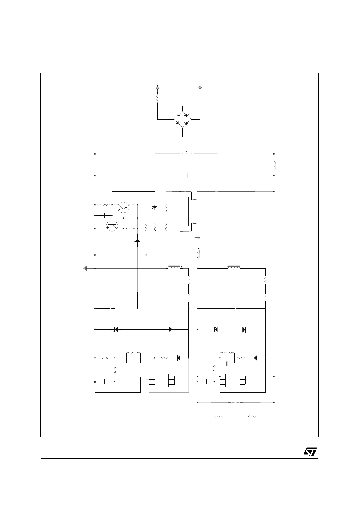
2. ELECTRICAL SCHEME
In Figure 1 the electrical scheme of 23W ballast is reported. The demo-board can be adapted to different
needs by connecting or not three jumpers.
Following the obtainable configurations:
1) Pre-heating function requested: J1, J2 closed, and J3 open;
2) Pre-heating not requested: J1, J2 open, J3 closed, C11, R1 1, D2, R7, R12 not mounted.
2.1 Circuit description
About the circuit description, the used topology was already described in the AN1546 and AN1694,
therefore in this paragraph only the main functions will be described.
The input sect ion is composed b y a fuse resist or R
and an input filter L1C2 that provide DC voltage and improve EMI performances according to IEC 610003-2 standard.
The net R13-R13_1-C13 connected to diac pin realizes the start-up while R7 (R8), D2 (D3), C11 (C12),
R11 (R12) perform the preheating function. The ballast working frequency is set by C7 and C8
capacitors. C9 is the snubber capacitor and R9, R9_1 are the pull-up resistor.
The net Q1, Q2, R14, R15, R16, C15, C16, D4, Dz1, detect the lamp failure (EoL) latching the converter.
The devices are synchronized and supplied by two secondary winding turned on ballast choke connect
with Sec pins by m eans input filter, R5, R5_1, C5 and R6, R6_1, C6, that provides a proper supply
voltage delaying the Sec pins vol tage com pared to th e sec ondary win ding vol tage in order t o av oid hard
switching condition.
a full bridge diode rectifier D1, a bulk capac itor C
0
0
September 2004 1/11
Page 2
AN2018 - APPLICATION NOTE
Figure 1: Electrical scheme.
N
R0
R16
Q1
C16
Q2
C13
C15
R15
Dz1
R14
R17
D4
D1
C2
R13
C4
R13_1
220V
C0
+
L1
TUBE
C3
TR-CFL
R6
R6_1
C6
Dz3
R12 C12
J3
J2
C8
D6
R8
D3
J1
VK05CFL
C7
TR
C5
Dz2
R11 C11
R9
D5
R7
VK05CFL
C9
R5
R5_1
D2
R9_1
2/11
Page 3

AN2018 - APPLICATION NOTE
2.2 Component list
In table 1 the material list for both circuits is reported.
Table 1: Component list 18W.
Reference Value Description
C0 4.7µF, 450V Electrolytic Capacitor
C2, C3 100nF, 400V Capacitor
C4 2.7nF, 400V 5% Start Up Capacitor
C5, C6, C7, C8 1,2nF, 63V SMD Capacitor
C9 470pF, 630V Snubber Capacitor
C11, C12 22µF, 35V Capacitor
C13, C15, C16 22nF, 63V SMD Capacitor
D1 SMD Bridge
D2, D3, D4, D5, D6 SMD Diode 1N4148
Dz1 12V Zener Diode
Dz2, Dz3 20V Zener Diode
IC1, IC2 STMicroelectronics VK05CFL
L1 820µH Inductor
Q1 Transistor PNP MPSA92A
Q2 Transistor NPN MPSA42A
R0 22Ω 1W Fuse Resistor
R5, R5_1, R6, R6_1 1KΩ 1/4W 5% SMD Resistor 1206
R7, R8 10KΩ SMD Resistor
R14, R17 27KΩ SMD Resistor
R11, R12 1MΩ SMD Resistor
R9, R9_1, R13, R13_1 510KΩ 200V SMD Resistor 1206
R15, R16 33KΩ SMD Resistor
T1 2.1 mH N1/N2=10:1 5% Resonant Inductor VOGT (Drawing: LL001 023 21)
Table 2: Component list 23W.
Reference Value Description
C0 6.8µF, 350V Electrolytic Capacit or
C2, C3 100nF, 400V Capacitor
C4 2.7nF, 400V 5% Start Up Capacitor
C5, C6 1nF, 63V SMD Capacitor
C7, C9 1nF SMD Capacitor
C9 470pF, 630V Snubber Capacitor
C11, C12 10µF, 35V Capacitor
C13, C15, C16 22nF, 63V SMD Capacitor
D1 SMD Bridge
D2, D3, D4, D5, D6 SMD Diode 1N4148
Dz1 13V Zener Diode
Dz2, Dz3 20V Zener Diode
IC1, IC2 STMicroelectronics VK05CFL
L1 1000µH Inductor
Q1 Transistor PNP MPSA92A
Q2 Transistor NPN MPSA42A
R0 22Ω 1W Fuse Resistor
R5, R5_1, R6, R6_1 1KΩ 1/4W 5% SMD Resistor 1206
R7, R8 9.1KΩ SMD Resistor
R14, R17 27KΩ SMD Resistor
R9, R9_1, R13, R13_1 510KΩ 200V SMD Resistor 1206
R11, R12 1MΩ SMD Resistor
R15, R16 33KΩ SMD Resistor
T1 2.1 mH N1/N2=10:1 5% Resonant Inductor VOGT (Drawing: LL001 023 21)
3/11
Page 4

AN2018 - APPLICATION NOTE
2.3 Start-up description
When a fluorescent lamp is switched on, the main voltage is not sufficient to cause the initial ionisation
and an element is needed to provide hi gh voltage across the tube. Ionised vapour radiates light in the
ultra-violet spectrum and is converted to visible light by a fluorescent coating inside the tube.
There are two methods to ignite the tube: cool ignition and warm ignition. Our ballast can perform both
methods.
Warm ignition is performed with the cathodes preheating; this method reduces the ignition voltage
improving the lamp life. During prehea ting time the tube p resents high impedanc e and the cu rrent flows
through the filaments growing their resistance value. There is a simple way to determine the right
preheating current/time valu e: the ratio b etween the cathode res istance before an d after t he preheat ing
has to be in the range 3 ÷ 5.
In our circuit the start-up network R13, R13_1, C13 is linked to DC bus by the lamp cathode in order to
guarantee automatic restart after lamp rep lacement. At s tart-up the ballast is in OF F state, when the
voltage on C13 reaches t he internal diac threshold (~ 30V ) the Low side device is turned ON mak ing the
current flow; the voltage drop on the main choke is transferred to secondary windings confirming the Low
side ON state and the High side OFF state respectively. In this phase the tube is an open circuit and
Lres-C4 fix the system resonance frequency.
2.4 Preheating description
If the cathodes' preheating is requested, our proposed solution performs this function in the following
way:
As soon as the sec pin voltage becomes positive, C11-C12 capacitors start to be charged adding current
into C7-C8 capacitors with Ton reduc tion and con sequent increasing in the working freque ncy. Since the
preheating network is applied on both devices the fifty percent of duty-cycle is guaranteed.
At the end of preheating time, af ter ignition occurs, the capacitors C11, C12, thanks to the presence of
diodes D2-D3, remain charged at the sec pin voltage stopping the current injection in C7 and C8. The
resistors R11, R12 discharge t he C11, C12 preheating capacitors allo wing a prehe ating phase when the
converter is switched-on again.
During preheating phase the working frequency is higher than the resonance one and the voltage across
the tube is lower than ignition one.
Adopting our preheating circuit, the current and frequenc y are variable during preheating phase, t his is
due to the fact the injected current is:
=(V
I
pre
sec-Vcappreh-Vfdiode
thus, this current decreases as the preheating capacitor voltage increases; in this way the working
frequency moves towards the resonance frequency in order to guarantee the tube ignition.
After this phase (I
=0) the preheating circuit and the ballas t frequency becom e steady state frequency
pre
fixed by C7, C8.
)/R
2.5 EoL description
The ballast shall not impair saf et y when abnormal and fault conditions happen. Abnorm al c ondition s are
classified (European standard) as:
- lamp not inserted
- the lamp does not start because one of the two cathodes are broken;
- the lamp does not start although the cathodes are intact (EoL);
- the lamp operates, but a single cathode is de-activated or broken (rectifying effect).
4/11
Page 5

AN2018 - APPLICATION NOTE
Third condition is a typical EoL situation and it is verified when the gas inside the tube is exhausted.
During the start-up phase, if the lamp doesn’t strike, very high current will flow in the circuit with
dangerous high voltage appearing across the tube. This anomaly can be damaging on base material also
resulting dangerous for the human operator that replaces the tube. For these reasons a protection
against faults is necessary. In order to detect EoL condition the method adopted is "voltage sensing
detection". In this case we detect an over voltage on Sec pin that activates a latch stopping the oscillation
in the ballast. The EoL protection is made monitoring the voltage across the low side preheating
capacitor C12. When the tube fails, th e voltage across the primary inductance and, consequently, the
voltage on secondary winding (with a ratio 10:1) raises with an increase in the C12 average voltage;
when Dz1 threshold voltage is reached, the latch circuit is activated switching the converter off. The main
latch functions are:
- Keeping sec pin voltage lower than its threshold by means of D4;
- Disable Diac function.
The latch sustaining c urrent is c om ing f rom R13. W it h this t echni que we are able t o m ain tain the cont rol
on the device current avoiding transformer core s aturation. Diodes D5 , D6, Dz2, Dz3 are added in 1 8W
and 23W demo-board in order to avoid negative over-voltage on Sec pins during EoL (See datasheet
VK05CFL for further details).
Figure 2: PCB photos
3. PCB DEFINITION
Figure 3: PCB Layout
PCB through hole component side (not in scale) PCB SMD component and copper side (not in
scale)
5/11
Page 6

AN2018 - APPLICATION NOTE
In layout design some simple rule have to be follow for components placement. The first one is related to
frequency capacitor placement that must to be moun ted as close as possible to the VK05CFL Osc pin;
and the second one is related to signal and power ground paths that have to be different in order to avoid
interference on the logic part.
Figure 4: Ground trace placement.
2
The copper area lived on the device collector for heat sink in this application is 1cm
4. EXPERIMENTAL RESULTS
The results have been obtained in the following conditions
a) Main voltage Vmain=230Vrms
b) Ambient temperature T
amb
=25 °C
c) Lamp power Plamp= 23W
.
4.1 Pre-heating
The pre-heating frequency i s 112KHz, it is higher than the resonance one f
C
=2.7nF). Pre-heating time is less than 1s, in this case pre-heating time is 880 ms and it is possible to
res
=66.8KHz (L
res
=2.1mH,
res
set it by changing C11-C12 capacitors and/or R7-R8 resistance. Figure 5 shows how the working
frequency starts to preheating one, and it moves towards resonance frequency during pre-heating phase
until ignition occurs; after that the working frequency is set by frequency capacitors.
Figure 5: Resonant curves.
6/11
Page 7

AN2018 - APPLICATION NOTE
Figure 6 shows the start up phase when pre-heating function is used.
Figure 6: Start-up phase. Ch1=Sec pin voltage; Ch2=diac pin voltage; Ch3=Mid point voltage;
Ch4=Choke current
Figure 7 shows the current and the voltage across the cathode during pre-heating. The cathode
resistance at the end of the preheating is about 3 times higher than its initial value ensuring the cathodes
heating.
Figure 7: Pre-heating phase Ch3= Cathode vo ltage; Ch4 Cathode current.
7/11
Page 8

AN2018 - APPLICATION NOTE
4.2 Steady state
In figure 8 the steady state waveforms are shown.
Figure 8 : Steady State Ch1=Sec pin v oltage; Ch2=Secondary winding voltage; Ch3 Mid p oint voltage;
Ch4=choke current.
The working frequency is 48 KHz with duty cycle of 49%. Using the proposed i nput filter the sec pin
voltage is higher than 4.5V at the end of Ton time.
4.3 En d of Life
In figure 9 choke current is shown. It is worth noting that the system goes in EOL condition a latching the
converter in 300ms, after preheating phase. Zener value can be tuning in order to modify the EOL
interv ention time.
Figure 9: EoL condition. Ch4= Choke c urrent
8/11
Page 9

AN2018 - APPLICATION NOTE
In figure 10 Sec pin voltage and voltage across the preheating capacitor (C12) are s hown. Negative Sec
pin voltage is clamped at -20V in order to avoid negative over voltage.
Figure 10: EoL condition. Ch1= Sec pin voltage, Ch3 = Preheating capacitor voltage.
4.5 THERMAL BEHAVIOUR
The thermal behavior analysis has been performed measuring the real devices temperature in
application, using thermocouples K type soldered on top of the packages.
The measurement has been performed driving a 23W tube at 55°C ambient temperature. In table 4
results are summarized distinguishing between low side and high side device temperature and copper
sink area.
Table 4:
Low side 97.5 63
High side 107.5 95
4.6. EMI and Harmonics current
Conducted EMI and Harmoni cs currents measurements h ave been performed according to EN55015
and IEC 61000-3-2.
The instruments used are: Agilent spectrum analyser and oscilloscope T ektronics.
In figure 11 current shape and Class D mask are shown, current is not sinusoidal than it has some
harmonics components at frequencies m ultiple than the fundamental. It is possible to ob serve that our
system fits class D specification according to IEC 61000-3-2.
Thermal behaviour analysis
VK05CFL Device Temperature (°C) Sink area (mm2)
9/11
Page 10

AN2018 - APPLICATION NOTE
Figure 11: Input current shape (normalized) and class D mask.
The conducted noise measurements have been performed on th e 23W at nominal 230Vac input voltage.
Results are shown in figure 12 and it is possible to notice that ballast passes the test on conducted
emissions according to EN55015.
Figure 12: Main terminals disturbance voltage: Conducted noise and EN55015 quasi peak limits.
10/11
Page 11

AN2018 - APPLICATION NOTE
Information furnished is believed to be accurate and reliable. However, STMicroelectronics assumes no responsibility for the consequences
of use of su ch in for mat i on n or f or a ny in fr ing em ent of pa te nts or o ther r igh ts of t hir d pa r tie s w hic h may res ul t f rom i ts us e. No license is granted
by impl i cation or ot herwise under any patent or patent r ig hts of STM i croelectronics. Specificat i ons mentio ned in this publicat ion are subject
to change wi t hout notice. Thi s publicati on supersedes and replaces all informat i on previou sly supplied . STMicroelectronic s products are not
authori zed for use as critical com ponents in l i fe support devices or systems without express written app roval of STM i croelectr o ni cs.
The ST logo i s a registered trademark of STMicr oel ectronics.
All other names are the property of their respective ow ners
© 2004 STMicroelectronics - A ll ri ghts res erved
STMicroelectronics group of companies
Australia - Belgium - Brazil - Canada - China - Czech Republic - Finland - France - Germany - Hong Kong - India - Israel - Italy - Japan -
Malaysia - Malta - Morocco - Singapore - Spain - Sweden - Switzerland - United Kingdom - United States of America
www.st.com
11/11
 Loading...