

Page 1
AN2002
APPLICATION NOTE
Usin g the Demoboard for the TD350 Advanc ed IGBT Driver
1 Introduction
TD350 is an advanced I GBT/MOSFE T driver with integrated cont rol and protection functi ons. Principles
of operation and application examples for the TD350 are described extensively in application note
AN1944. The presen t application note con cerns the characteristics a nd use of the dem oboard available
for testing the TD350.
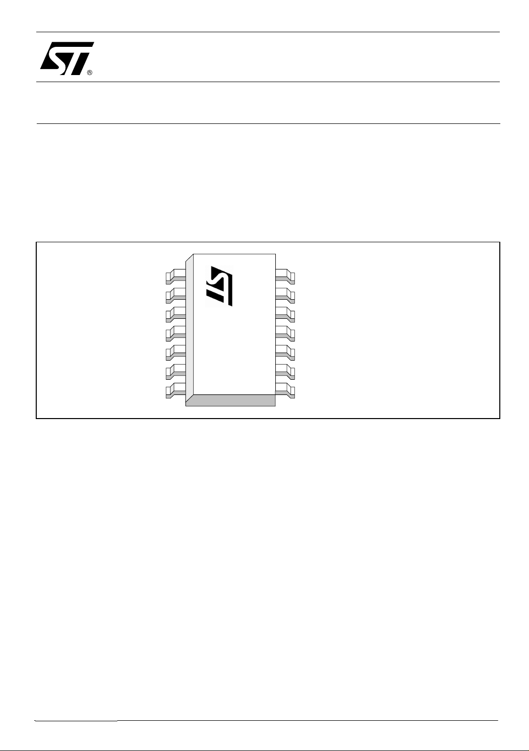
Figure 1: TD350 pinout
1
VREF
IN
2
14
13
DESAT
VH
NC
COFF
NC
LVOFF
3FAULT
4
5
6
7
date code
TD350I
12
11
10
9
8
OUT
OUTL
VL
CLAMP
GND
Bevelled edg e
indicates pin 1
location
2 Printed circuit board presentation
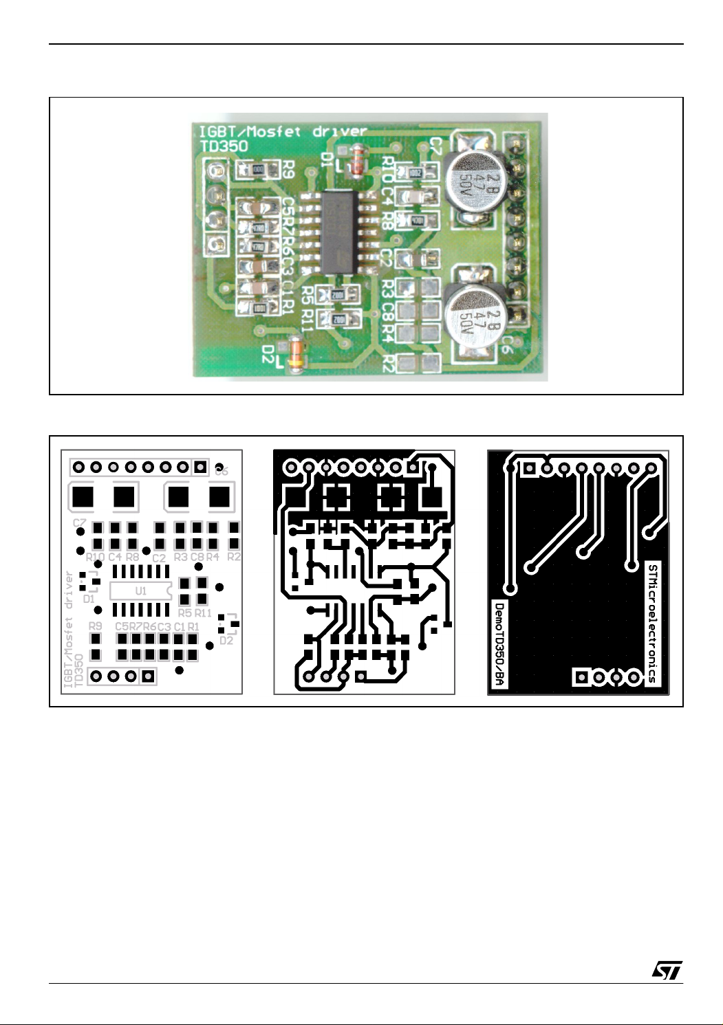
The demoboard is a 26x35mm double-sided PCB with the TD350 and its peripheral components
mounted in a typical configuration (pictured in Figure 2). To aid in the understanding and easy
modification of the board, the PCB top-side and bottom-side layers, as well as the silk-screen previews
are shown i n Figure 3.
The demoboard electrical schematic is presented on Figure 4, and the associate d bi ll o f material can be
found on Table 1 on page 5.
Let’s study step by step the demoboard original configuration, and the way it can be modified to be
adapted to the application.
July 2004
Revision A 1/8
Page 2
AN2002 Using the Demoboard for the TD350 Advanced IGBT Driver
Figure 2: Demoboard layout
Figure 3: Demoboard PCB: Silk-screen, top-layer an d bottom -layer previews
2.1 Input stage
The TD350 can be drive n by either a pulse transformer or an optocoupler. The dem oboard is set up to
use an optoc oupler. The T D350 IN pin i s clamped t o 5V by a zener diode D2 and its bleeding resistor
R11=10K (see demoboa rd schematic on Fi gure 4). To interface the demoboard with the system, the IN1
pin of the input connector can simply be connected to a low-side optocoupler, as show on Figure 5. An
optional filtering capacitor can be added (for instance 47pF) in the event of a highly noisy environment,
although the TD350 already includes a filtering o n input signals and reject s signals smaller than 1 00ns
specification).
(t
onmin
The demoboard can be modified to be driven by a pulse transformer by implementing the optional
components R2, R3, R4 and C8. The principle of operation with a pulse transformer is explained in
AN1944.
2/8
Page 3

Using the Demoboard for the TD350 Advanced IGBT Driver AN2002
VH
GNDVLOUTL
2.2 Output stage
The TD350 uses separate sink and source outputs (OUTL/OUTH ) for easy gate driving. The integrated
circuit output stage is able to sink/source about 2A/1.5A typical at 25°C, but the IGBT turn-on and turn-off
current can be limited independently by the g ate resistors R6 and R7 includ ed on the demoboard. The
original value for these resistors are R6=R7=47R.
Output current capability can be increased by using an external buffer with two low-cost bipolar
transistors. This configuration is described in Section 4 on page 7.
2.3 Active Miller Clamp
The TD350 offers an alternative solution to the problem of the Miller current in IGBT switching
applications. Instead of driving the IGBT gate to a negative voltage to increase the safety margin, the
TD350 uses a dedicated CLAMP pin to control the Miller current. When the IGBT is off, a low impedance
path is established between IGBT gate and em itter to carry the Miller current, and the voltage spike on
the IGBT gate is greatly reduced. The CLAMP switch is opened when the input is activated and is closed
when the actua l gate voltage goes close to the ground level. In th is way, the CLAMP funct ion doesn’t
affect the turn-off characteristic, but only keeps the gate to the low level throughout the off time.
On the demoboard, the CLAMP pin is connected to the IGBT gate by strap R9. This strap can be
removed when the clamp feature is not needed, or when an external buffer is used (see reference
schematic on Figure 6).
Figure 4: Demoboard PCB: Electrical Schematic
VH
R6
R7
C1
C3
C5 C7
R1
VH
C6
R9
VL
1
2
3
4
Desat
Out
Gnd
Clamp
Gnd
Fault
Gnd
Lvoff
In2
VH
In1
R2*
1
2
3
4
5
6
7
VL
VL
8
C8*
VH
R3*
C2VH
R4*
R5
VREF
R8
C4
R10
D1
(*): optional parts not m ounted on demoboard original configurati on
R11
D2
TD350
IN
1
VREF
2
FAULT
3
NC
4
COFF
5
NC
6
LVOFF
7
DESAT
OUTH
CLAMP
14
13
12
11
10
9
8
2.4 2-level turn-off
In the event of a short-circuit or overcurrent in the load, a large voltage overshoot can occur across the
IGBT at turn-off and can ex ceed t he IGB T breakdown voltage. By reducing the ga te voltag e bef ore turnoff, the IGBT current i s limited a nd the pote ntial overvoltage is redu ced. Thi s technique is called 2-level
turn-off. Both the level and duration of the intermediate off level are adjustable. Duration is set by the
external resistor R8 and capacitor C4 i n conjunction with the integrated voltage reference for accurat e
3/8
Page 4

AN2002 Using the Demoboard for the TD350 Advanced IGBT Driver
timing. The level can be easily set by an ext ernal Zener diode D1, and its v alue is chos en depending on
the IGBT characteristics. This 2-level turn-off sequence takes place at each cycle, it has no effect if the
current doesn’t exceed the normal m aximum rated value, but protects the IGBT in case of overcurrent
(with a slight increase of conduction losses).
In the demoboard original configuration, Ta (duration of the intermediate level) is set to approximately
1.5µs by R8 =4K7 and C4=470pF. The i ntermediate level is set by 1 0V Zener diode D1 and b leeding
resistor R11=10K.
Tip: How can you inhibit 2-level turn-off?
Connect LVOFF to VH b y replacing R10 by a short-circuit, remove C 4 capacitor and keep
COFF pin connected to Vref by R8=4K7.
2.5 Desaturation protection feature
The desaturation function provide s a protection against overcurrent events. Voltage ac ross the IGBT is
monitored, and the IGBT is turned off if the vo ltage th reshold is reached. A blanking time, t
an internal 250mA c urrent source a nd an ex ternal capacitor C1. The DES AT pin is con nected t o output
demoboard connector by R1 resistor. In order to implement the desaturation feat ure, an external high
voltage diode (1kV or more) should be connected between the IGBT collector and the demoboard output
connector pin 1 (see Figure 6 for reference schematic).
, is set using
b
The high voltage diode blocks the high voltage during IGBT off state. This diode doesn’t need to be fast,
a standard 1kV (or more) diode is acceptable.
During operation, the DESAT capacitor is discharged when TD350 out put is low (IGBT off). When the
IGBT is turned on, the DE SAT capac itor starts c harging and desat uration protec t ion is effective after the
blanking time, t
With the capacitor used in the demoboard (C1=100pF), the blanking time value will be close to 3ms.
Tip: What should one do with the DESAT pin when it isn’t used?
, has elapsed:
b
C
1
t
7.2V
b
Connect DESAT to GND by shorting together pin 1 and pin 3 on the demoboard output
connector (see Figure 5).
----------------- -Þ=
250µA
4/8
Page 5

Using the Demoboard for the TD350 Advanced IGBT Driver AN2002
Table 1: Bill of materials f or demoboard
Designator Description Value Package
R1 desaturation resistor 1K-1% 0805
C1 desaturation filtering capacitor 100pF-X7R 0805
C3 positive supply ceramic decoupling capacitor 100nF-X7R 0805
C5 negative supply ceramic decoupling capacitor 100nF-X7R 0805
C6 positive supply electrolytic capacitor 47
C7 negative supply electrolytic capacitor 47
R6 turn-on gate drive resistor 47R-1% 0805
R7 turn-off gate drive resistor 47R-1% 0805
R9 strap (optional) 0R 0805
R11 bleeding resistor for Zener diode D2 10K-1% 0805
C2 Vref decoupling capacitor 10nF-X7R 0805
R5 FAULT pin pull-up resistor 10K-1% 0805
R8 2-level turn-off timing resistor 4K7-1% 0805
C4 2-level turn-off timing capacitor 470pF-X7R 0805
R10 bleeding resistor for Zener diode D1 10K-1% 0805
D1 Zener diode for 2-level turn-off intermediate level programming 10V Melf
D2 Zener diode for IN pin level 5V1 Melf
U1 IGBT/MOSFET driver TD350 SO-14
µF-50V d6.3 x h7.7
µF-50V d6.3 x h7.7
J1 Input connector 8-lead
J2 Output connector 4-lead
C8 Vref/2 filtering capacitor not mounted 0805
R4 Vref/2 divider bridge lower resistor (only with pulse transformer) not mounted 0805
R3 Vref/2 divider bridge upper resistor (only with pulse transformer) not mounted 0805
R2 adjustment resistor (only with pulse transformer) not mounted 0805
5/8
Page 6

AN2002 Using the Demoboard for the TD350 Advanced IGBT Driver
3 Application example no. 1
This first application example demonstrates the typical configuration in which TD350 can be used in low
and medium power applications. In this configuration, the TD350 is able to drive IGBTs with current
ratings up to about 50A. The schematic showing how to connect the demoboard to the optocoupler,
power supply and IGBT module is presented on Figure 5. The demoboard doesn’t require any
modification in order to be used in this configuration. However, it should be noted that C5 and C7
(decoupling capacitors for negative supply) are not needed in this example and they could be removed to
optimize application cost and PCB space.
The main characteristics of this example are:
l
Single S upply: w ith the benefit of the Active Miller Clamp feature, n egative supply isn’t need ed to
avoid mistriggering of the IGBT at turn-off
l
Active Miller Clamp: the feature is implem ented on the demoboard by conne cting TD350 CLAMP
pin to the IGBT gate with R9=0R resistor
l
2-Step Turn-Off: at turn-off the gate-to-source voltage will be lowered to 10V during approximately
1.5µs to reduce over-voltage stress on the IGBT in case of over-current event
l
DESAT not used: to simplify the design DESAT pin is connected to GND to inhibit the function. To
implement the desaturation protection, see Section 2.5.
Figure 5: TD350 demoboard used in basic application
6/8
47pF*
16V
In2
1
VH
2
Gnd
3
In1
4
Fault
5
Gnd
6
VL
7
8
Lvoff
(*): opt i on al part s
TD350 de m o bo a rd
Desat
Out
Gnd
Clamp
1
2
3
4
Page 7

Using the Demoboard for the TD350 Advanced IGBT Driver AN2002
Desat
Clamp
4 Application example no.2
This second application example shows the typical configuration in which the TD350 can be used in high
power applications. With the use of an additional buffer, the TD350 can drive IGBTs with a current rating
above 100A. The schematic in Figure 6 shows how to connect the demoboard with the optocoupl er and
the power supplies o n t he i nput side, and with the IGBT module and the gate buffer circuit on th e output
side.
The demoboard n eeds a few m odif ications wi th respec t to its original conf iguration to be us ed as s ho wn
in this example:
1)The R9 strap should be removed.
2)The resistors R6 and R7 should be replaced by short-circuits.
The main characteristics of this example are:
l
A dual supply +16V/-10V is used as often needed in high power applications,
l
Output buffer stage: considering the high val ue of the IGBT gate c apacitanc e, t he TD350 output is
connected to a discrete buffer stage made of two complementary bipolar transistors,
l
CLAMP used as secondary gate discharge: the CLAMP pin is connected to a external buffer to
feature a secondary gate discharge,
l
DESAT feature is implemented.
Figure 6: TD350 demoboard used in high power applications
In2
47pF*
16V
10V
1
2
3
4
5
6
7
8
TD350 demoboard
VH
Gnd
In1
Fault
Gnd
VL
Lvoff
(*): opti onal part s
Out
Gnd
1
2
3
4
1kV
diode
VH
T1
T2
VL
T3
VL
7/8
Page 8

AN2002 Using the Demoboard for the TD350 Advanced IGBT Driver
Information furnished is believed to be accurate and reliable. However, STMicroelectronics a ssumes no responsibility for the
consequences of use of such information nor for any infringement of patents or other rights of third parties which may result from
its use. No license i s granted by implication or ot herwise under any patent or patent rights of STMi croe lectr onics. S pecifications
mentioned in this publication are subject to change without notice. This publicatio n supersedes and replaces all information
previously supplied. STMicroe lectronics products are not aut horized for use as cr itical components in life su pport devices or
systems without express written approval of STMicroelectronics.
The ST logo is a registered trademark of STMicroelectronics
All other n ames are the property of the ir respective owners
© 2004 STMicroelectronics - All Rights Reserved
Australi a - Belgium - Brazil - Canad a - China - Czech Repubic - Fi nl and - France - Germany - Hong Kong - India - Israel - Italy - Japan
Malaysia - M al ta - Morocco - Singapore - Sp ai n - Sweden - Switzerland - United Kingdom - United S tates
STMicroelectronics GROUP OF COMPANIES
www.st.com
8/8
 Loading...