

Page 1
AN2001
Obsolete Product(s) - Obsolete Product(s) Obsolete Product(s) - Obsolete Product(s)
Application note
VIPower: VIPer53 single output reference
board 90 to 264 VAC input, 24W output
Introduction
The VIPer53 combines an enhanced current mode PWM controller with a high voltage
MDMesh Power Mosfet in the same package. VIPer53 is available in two different
packages, DIP-8 and PowerSO-10. This reference board is an offline wide range power
supply that incorporates VIPer53 and is set up for secondary regulation by driving the PWM
controller through an optocoupler. The switching frequency is set at 100 kHz and the total
output power is 24W.
● Switch mode general purpose power supply
● Current mode control with adjustable limitation
● 75% efficiency
● Output short circuit and overload protection
● Thermal shutdown protection
● Meets EN55022 class B EMI specification
● Blue Angel compliant
Operating conditions
Parameter Limits
Input voltage range 90 to 264Vac
Input Frequency 100kHz
Output voltage V=12V
Output power 24W
Efficiency 75% typical
Line regulation +/- 0
Load regulation +/- 0.2%
Output ripple voltage 15mVpp
EMI EN55022 Class B
September 2006 Rev 2 1/19
www.st.com
Page 2

Obsolete Product(s) - Obsolete Product(s) Obsolete Product(s) - Obsolete Product(s)
Contents AN2001
Contents
1 PCB lay-out . . . . . . . . . . . . . . . . . . . . . . . . . . . . . . . . . . . . . . . . . . . . . . . . 5
2 Efficiency . . . . . . . . . . . . . . . . . . . . . . . . . . . . . . . . . . . . . . . . . . . . . . . . . . 6
3 Load regulation . . . . . . . . . . . . . . . . . . . . . . . . . . . . . . . . . . . . . . . . . . . . . 7
4 Line regulation . . . . . . . . . . . . . . . . . . . . . . . . . . . . . . . . . . . . . . . . . . . . . . 8
5 Transient response . . . . . . . . . . . . . . . . . . . . . . . . . . . . . . . . . . . . . . . . . . 9
6 Line and switching frequency ripple . . . . . . . . . . . . . . . . . . . . . . . . . . . 10
7 Waveforms . . . . . . . . . . . . . . . . . . . . . . . . . . . . . . . . . . . . . . . . . . . . . . . . 11
8 Blue Angel . . . . . . . . . . . . . . . . . . . . . . . . . . . . . . . . . . . . . . . . . . . . . . . . 12
9 EMI results . . . . . . . . . . . . . . . . . . . . . . . . . . . . . . . . . . . . . . . . . . . . . . . . 13
10 Transformer specification . . . . . . . . . . . . . . . . . . . . . . . . . . . . . . . . . . . 14
11 Different output current and voltage capability . . . . . . . . . . . . . . . . . . 15
12 Revision history . . . . . . . . . . . . . . . . . . . . . . . . . . . . . . . . . . . . . . . . . . . 18
2/19
Page 3

Obsolete Product(s) - Obsolete Product(s) Obsolete Product(s) - Obsolete Product(s)
AN2001 List of figures
List of figures
Figure 1. Board layout (not in scale) . . . . . . . . . . . . . . . . . . . . . . . . . . . . . . . . . . . . . . . . . . . . . . . . . . 5
Figure 2. Efficiency vs. Iout . . . . . . . . . . . . . . . . . . . . . . . . . . . . . . . . . . . . . . . . . . . . . . . . . . . . . . . . . 6
Figure 3. Efficiency vs. Vin. . . . . . . . . . . . . . . . . . . . . . . . . . . . . . . . . . . . . . . . . . . . . . . . . . . . . . . . . . 6
Figure 4. Load regulation . . . . . . . . . . . . . . . . . . . . . . . . . . . . . . . . . . . . . . . . . . . . . . . . . . . . . . . . . . . 8
Figure 5. Line regulation . . . . . . . . . . . . . . . . . . . . . . . . . . . . . . . . . . . . . . . . . . . . . . . . . . . . . . . . . . . 8
Figure 6. Transient response . . . . . . . . . . . . . . . . . . . . . . . . . . . . . . . . . . . . . . . . . . . . . . . . . . . . . . . . 9
Figure 7. Line frequency ripple . . . . . . . . . . . . . . . . . . . . . . . . . . . . . . . . . . . . . . . . . . . . . . . . . . . . . 10
Figure 8. Switching frequency ripple . . . . . . . . . . . . . . . . . . . . . . . . . . . . . . . . . . . . . . . . . . . . . . . . . 10
Figure 9. V
Figure 10. EMI . . . . . . . . . . . . . . . . . . . . . . . . . . . . . . . . . . . . . . . . . . . . . . . . . . . . . . . . . . . . . . . . . . 13
Figure 11. Transformer specifications . . . . . . . . . . . . . . . . . . . . . . . . . . . . . . . . . . . . . . . . . . . . . . . . . 14
Figure 12. PC board top legend (not in scale) . . . . . . . . . . . . . . . . . . . . . . . . . . . . . . . . . . . . . . . . . . . 15
Figure 13. PC board bottom copper (not in scale) . . . . . . . . . . . . . . . . . . . . . . . . . . . . . . . . . . . . . . . . 15
Figure 14. Schematic diagram . . . . . . . . . . . . . . . . . . . . . . . . . . . . . . . . . . . . . . . . . . . . . . . . . . . . . . . 17
and drain current . . . . . . . . . . . . . . . . . . . . . . . . . . . . . . . . . . . . . . . . . . . . . . . . . . . . . 11
ds
3/19
Page 4

Obsolete Product(s) - Obsolete Product(s) Obsolete Product(s) - Obsolete Product(s)
List of tables AN2001
List of tables
Table 1. Secondary component value to obtain different output voltage and current. . . . . . . . . . . . 15
Table 2. Component list . . . . . . . . . . . . . . . . . . . . . . . . . . . . . . . . . . . . . . . . . . . . . . . . . . . . . . . . . . 15
Table 3. Revision history . . . . . . . . . . . . . . . . . . . . . . . . . . . . . . . . . . . . . . . . . . . . . . . . . . . . . . . . . 18
4/19
Page 5
Obsolete Product(s) - Obsolete Product(s) Obsolete Product(s) - Obsolete Product(s)
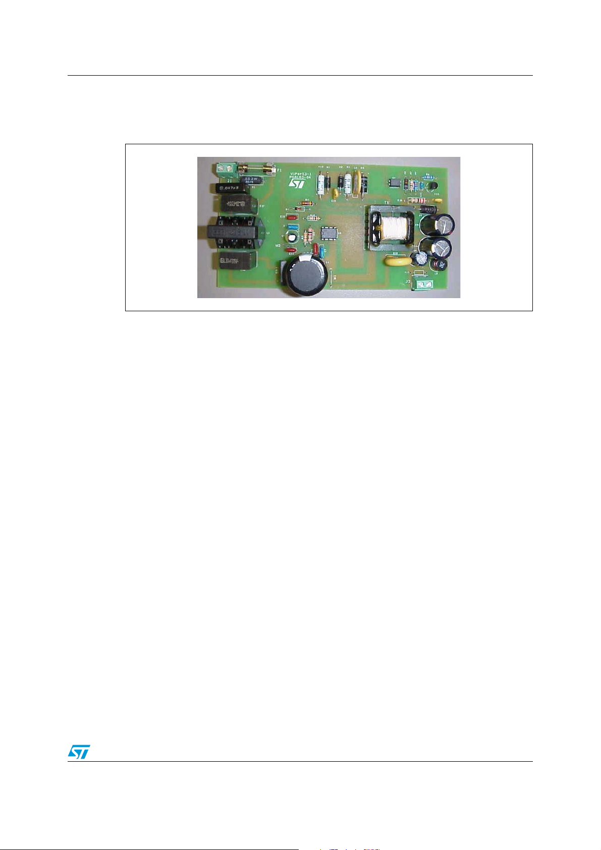
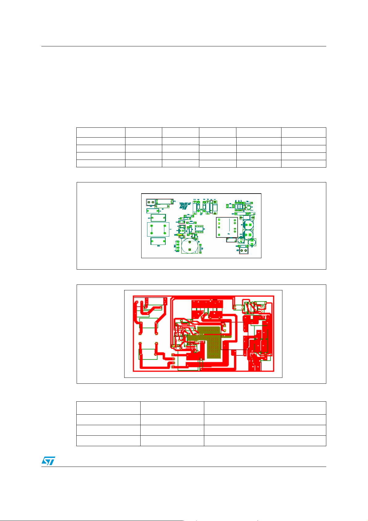
AN2001 PCB lay-out
1 PCB lay-out
Figure 1. Board layout (not in scale)
5/19
Page 6
Obsolete Product(s) - Obsolete Product(s) Obsolete Product(s) - Obsolete Product(s)
Efficiency AN2001
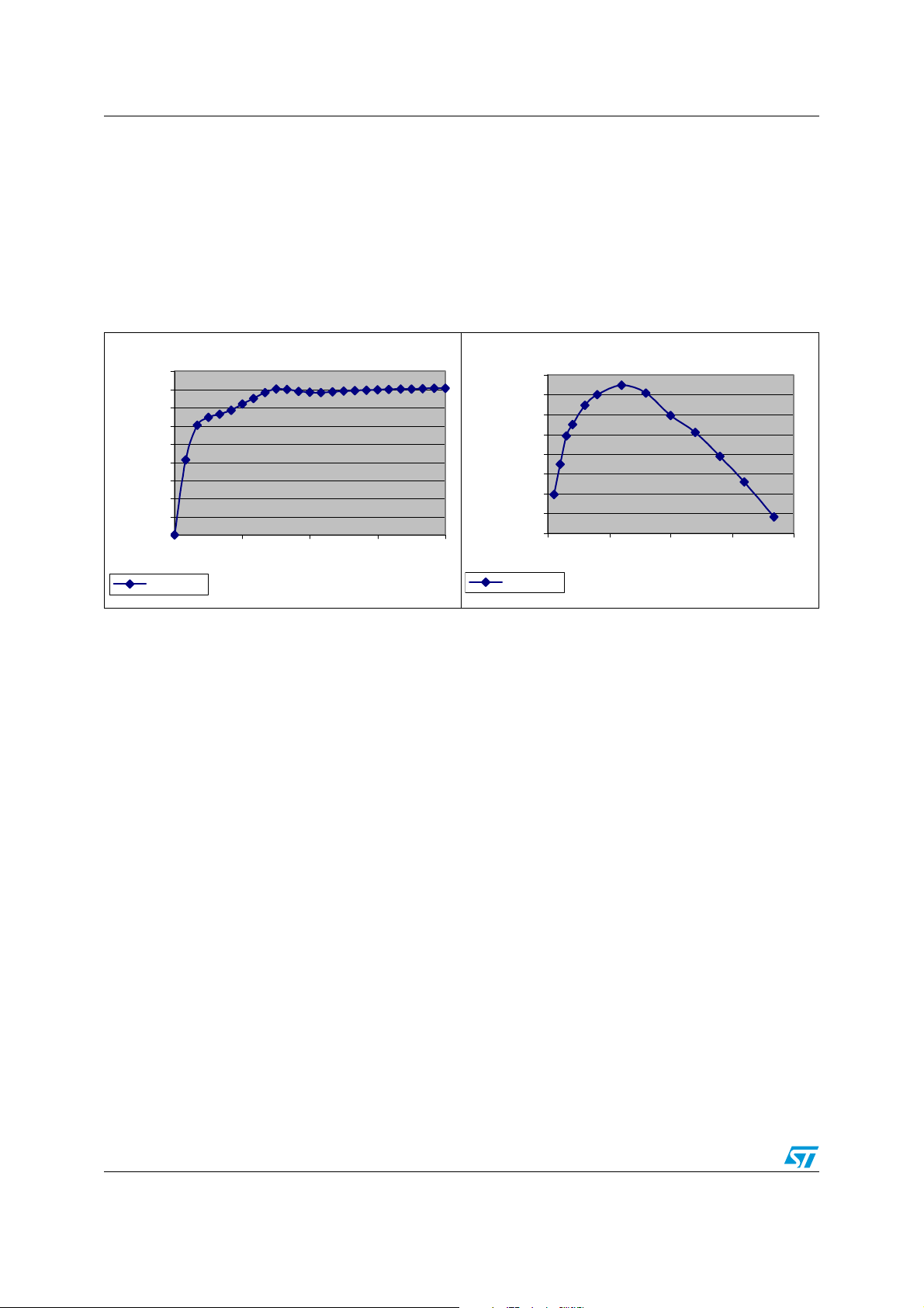
2 Efficiency
Figure 2. and Figure 3. shows the two efficiency curves of the reference board. The
measurements on Figure 2. are taken at the input voltage of 120Vac while the output load is
varied from 0A to the full load of 2A. Meanwhile, Figure 3. shows the efficiency when the
input voltage is varied from 90 to 264Vac while the output load is fixed at 2A.
Figure 2. Efficiency vs. Iout Figure 3. Efficiency vs. Vin
90%
80%
70%
60%
50%
40%
30%
Efficiency (%)
20%
10%
0%
00.511.52
Efficiency
Iout (A)
81.00%
80.50%
80.00%
79.50%
79.00%
78.50%
Efficiency (%)
78.00%
77.50%
77.00%
Efficiency
80 130 180 230 280
Vin (Vac)
6/19
Page 7

Obsolete Product(s) - Obsolete Product(s) Obsolete Product(s) - Obsolete Product(s)
AN2001 Load regulation
3 Load regulation
Vout is measured while the output load is varied from 0A to 2A at the nominal input voltage
of 120Vac. Figure 4. shows the load regulation measured, which is 0.2%.
7/19
Page 8

Obsolete Product(s) - Obsolete Product(s) Obsolete Product(s) - Obsolete Product(s)
Line regulation AN2001
4 Line regulation
The line regulation is measured to be 0%. Here, the output load is kept at the full load of 2A
while the input voltage is varied from 90 to 264V and the output voltage for the reference
board remains regulated.
Figure 4. Load regulation Figure 5. Line regulation
12.5
12.4
12
11.5
11
Vout (V)
10.5
10
00.511.52
Iout (A)
12.2
12
Output Voltage (V)
11.8
90 140 190 240 290
Input Voltage (Vac)
8/19
Page 9

Obsolete Product(s) - Obsolete Product(s) Obsolete Product(s) - Obsolete Product(s)
AN2001 Transient response
5 Transient response
Figure 6. Transient response
Figure 6. shows the transient load response as the output load is stepped from 1A to 2A
(50% to 100% load) at the input voltage of 120Vac. The dynamic response is 80mV or 0.7%
while the settling time is found to be 420µs.
9/19
Page 10
Obsolete Product(s) - Obsolete Product(s) Obsolete Product(s) - Obsolete Product(s)
Line and switching frequency ripple AN2001
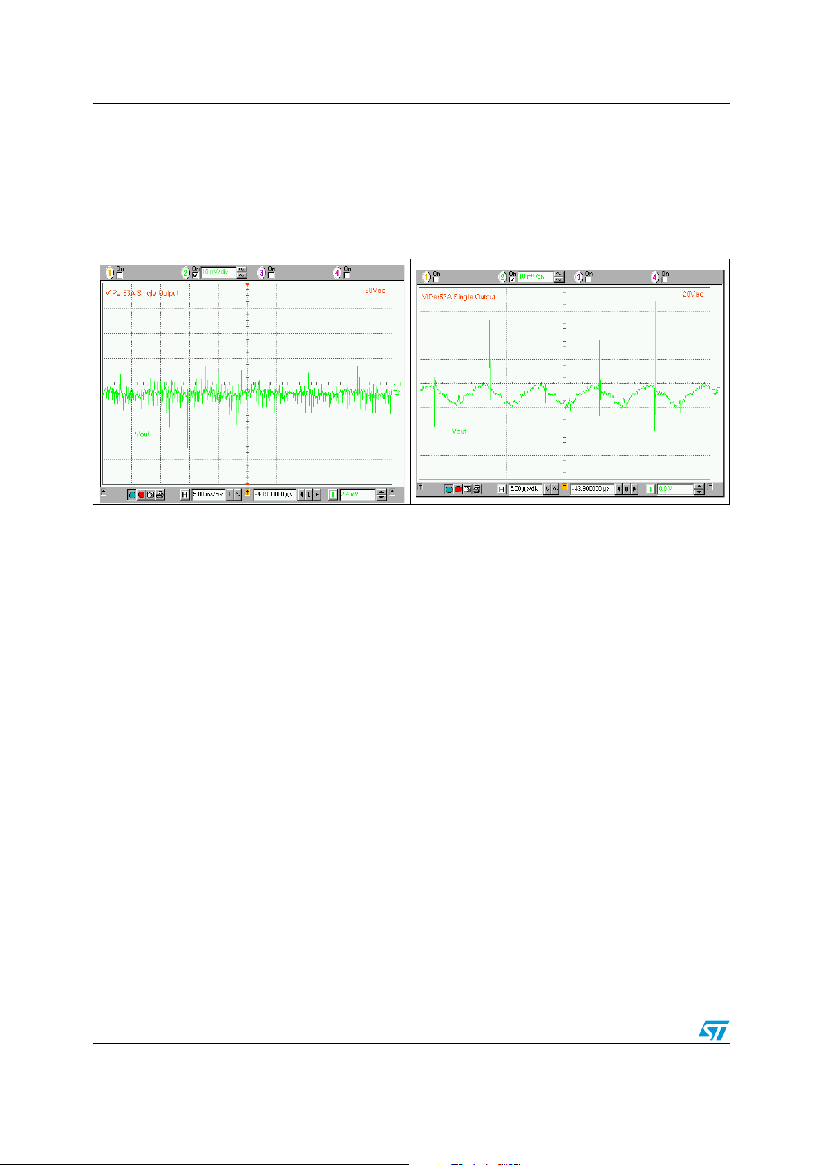
6 Line and switching frequency ripple
Figure 7. and Figure 8. show the line and switching frequency ripple of the reference board
measured at the input voltage of 120Vac and the output current is fixed at 2A.
Figure 7. Line frequency ripple Figure 8. Switching frequency ripple
Both waveforms show a line frequency and switching frequency ripple of 10mVpp each.
10/19
Page 11

Obsolete Product(s) - Obsolete Product(s) Obsolete Product(s) - Obsolete Product(s)
AN2001 Waveforms
7 Waveforms
Figure 9. shows the drain current and Vds at 230Vac full load. The converter is working in
discontinuous mode as can be seen from the waveforms.
Figure 9. V
and drain current
ds
11/19
Page 12

Obsolete Product(s) - Obsolete Product(s) Obsolete Product(s) - Obsolete Product(s)
Blue Angel AN2001
8 Blue Angel
The reference board consumes less than 1W total when working in stand-by burst mode at
the input voltage of 120Vac. The measured input power consumption is 569mW with zero
loads at the output.
Therefore, the board meets Blue Angel norm.
12/19
Page 13

Obsolete Product(s) - Obsolete Product(s) Obsolete Product(s) - Obsolete Product(s)
AN2001 EMI results
9 EMI results
Figure 10. EMI
The reference board passes the EN55022 Class B EMI test as shown in Figure 10.
13/19
Page 14
Obsolete Product(s) - Obsolete Product(s) Obsolete Product(s) - Obsolete Product(s)
Transformer specification AN2001
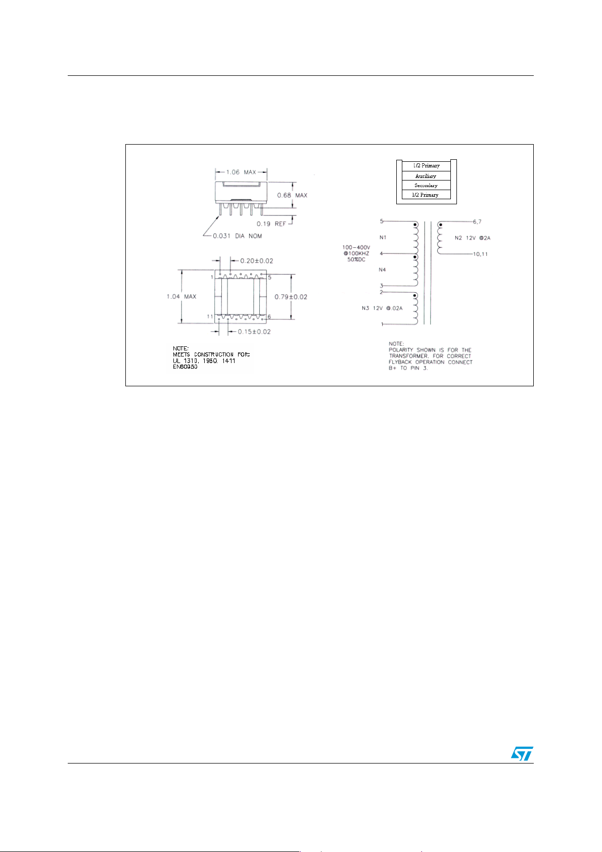
10 Transformer specification
Figure 11. Transformer specifications
The transformer is designed and manufactured by Cramer Coil and Transformer Co., Inc.
The electrical characteristics of the transformer are as follows:
The electrical specifications of the transformer are as follow
● Primary Inductance 1.10mH±10%
● Primary Leakage Inductance 6.4µH typical
● HIPOT (N1, N3, N4 tro N2) 4000VAC, 1sec
● DCR (N1/N4) 0.905 Ω typical
● DCR (N2) 0.020 Ω typical
● DCR (N3) 0.112 Ω typical
● Turns Ratio (N1/N4:N2) 1:0.121±3%
● Turns Ratio (N1/N4:N3) 1:0.121±3%
When VIPer53 is on, energy is stored in the primary winding of the transformer (pins 3-5).
This energy is transferred to the auxiliary winding (pins 1-2), and to the output (6, 7-10, 11)
when the VIPer53 is off. The auxiliary winding provides the bias voltage for the VIPer53 at
pin 7 (Vdd).
:
14/19
Page 15
Obsolete Product(s) - Obsolete Product(s) Obsolete Product(s) - Obsolete Product(s)
AN2001 Different output current and voltage capability
11 Different output current and voltage capability
The standard voltage and current values for the reference board can be changed to deliver a
different voltage and current value, with changes to the following components as detailed in
Table 1.
Table 1. Secondary component value to obtain different output voltage and
current
Vout and Iout T1 R6 R9 C8, C16 D4
5.0V 4.8A CVP53-003 2.49kΩ 1% 2.49kΩ 1% 3300µF 10V STPS1045
12V 2.0A CVP53-001 3.48kΩ 1% 13.3kΩ 1% 1000µF 25V BYW98-200
15V 1.6A CVP53-004 2.94kΩ 1% 14.7kΩ 1% 1000µF 35V BYW98-200
24V 1.0A CVP53-005 1.50kΩ 1% 13.0kΩ 1% 470µF 50V BYW98-200
Figure 12. PC board top legend (not in scale)
Figure 13. PC board bottom copper (not in scale)
Table 2. Component list
Quantity Reference Description
1 BR1 KBP210GDI bridge rectifier
1 C1 0.047µF 250V boxcap
1 C2 68µF/400V electrolytic
15/19
Page 16

Obsolete Product(s) - Obsolete Product(s) Obsolete Product(s) - Obsolete Product(s)
Different output current and voltage capability AN2001
Table 2. Component list
Quantity Reference Description
1 C3 4700pF 1kV ceramic
1 C4 100µF/25V electrolytic
1 C5 4.7nF 50V polyester
2 C6, C7 470nF 50V ceramic
2 C8, C16 1000µF/25V electrolytic
1 C9 220µF/25V electrolytic
1 C10 4.7nF/250V Y1 cap
2 C11, C12 0.01µF 50V ceramic
1 C13 470pF/1kV ceramic
1 C14 100pF/1kV ceramic
1 C15 Not used
2 C17, C18 0.33µF/250V boxcap
1 L1 Panasonic 35mH common-mode line choke
1 L2 Coilcraft 2.2µH inductor
1 T1 Cramer Coil CVP53-001
1R1 4Ω 5% 3W Wire wound
1R2 22kΩ 5% 2W resistor
1R3 3kΩ 5% 0.5W resistor
1R4 15Ω 5% 0.25W resistor
1R53.3kΩ 5% 0.25W resistor
1 R6 3.48kΩ 1% 0.25W resistor
1R7 1kΩ 5% 0.25W resistor
1R8 68Ω 5% 0.25W resistor
1 R9 13.3kΩ1% 0.25W resistor
1 R10 22Ω 5% 0.5W resistor
1 R12 1kΩ 5% 2W resistor
1 R13 Not used
1D1 1N4148
2 D2, D3 STMicroelectronics STTH1R06
1 D4 STMicroelectronics BYW98-200
1 D5 STMicroelectronics 1.5KE220A transil
1 U2 H11A817A or LTV817A optocoupler
1 U3 STMicroelectronics TL431
1 U4 STMicroelectronics VIPer53DIP
16/19
Page 17

Obsolete Product(s) - Obsolete Product(s) Obsolete Product(s) - Obsolete Product(s)
AN2001 Different output current and voltage capability
Table 2. Component list
Quantity Reference Description
2 W1, W2 Jumper wire
2 J1, J2 Connectors
Figure 14. Schematic diagram
4
17/19
Page 18

Obsolete Product(s) - Obsolete Product(s) Obsolete Product(s) - Obsolete Product(s)
Revision history AN2001
12 Revision history
Table 3. Revision history
Date Revision Changes
16-Jul-2004 1 First issue
- New template
12-Sep-2006 2
- Component list value modified
- Schematic diagram modified
18/19
Page 19

Obsolete Product(s) - Obsolete Product(s) Obsolete Product(s) - Obsolete Product(s)
AN2001
Please Read Carefully:
Information in this document is provided solely in connection with ST products. STMicroelectronics NV and its subsidiaries (“ST”) reserve the
right to make changes, corrections, modifications or improvements, to this document, and the products and services described herein at any
time, without notice.
All ST products are sold pursuant to ST’s terms and conditions of sale.
Purchasers are solely responsible for the choice, selection and use of the ST products and services described herein, and ST assumes no
liability whatsoever relating to the choice, selection or use of the ST products and services described herein.
No license, express or implied, by estoppel or otherwise, to any intellectual property rights is granted under this document. If any part of this
document refers to any third party products or services it shall not be deemed a license grant by ST for the use of such third party products
or services, or any intellectual property contained therein or considered as a warranty covering the use in any manner whatsoever of such
third party products or services or any intellectual property contained therein.
UNLESS OTHERWISE SET FORTH IN ST’S TERMS AND CONDITIONS OF SALE ST DISCLAIMS ANY EXPRESS OR IMPLIED
WARRANTY WITH RESPECT TO THE USE AND/OR SALE OF ST PRODUCTS INCLUDING WITHOUT LIMITATION IMPLIED
WARRANTIES OF MERCHANTABILITY, FITNESS FOR A PARTICULAR PURPOSE (AND THEIR EQUIVALENTS UNDER THE LAWS
OF ANY JURISDICTION), OR INFRINGEMENT OF ANY PATENT, COPYRIGHT OR OTHER INTELLECTUAL PROPERTY RIGHT.
UNLESS EXPRESSLY APPROVED IN WRITING BY AN AUTHORIZED ST REPRESENTATIVE, ST PRODUCTS ARE NOT
RECOMMENDED, AUTHORIZED OR WARRANTED FOR USE IN MILITARY, AIR CRAFT, SPACE, LIFE SAVING, OR LIFE SUSTAINING
APPLICATIONS, NOR IN PRODUCTS OR SYSTEMS WHERE FAILURE OR MALFUNCTION MAY RESULT IN PERSONAL INJURY,
DEATH, OR SEVERE PROPERTY OR ENVIRONMENTAL DAMAGE. ST PRODUCTS WHICH ARE NOT SPECIFIED AS "AUTOMOTIVE
GRADE" MAY ONLY BE USED IN AUTOMOTIVE APPLICATIONS AT USER’S OWN RISK.
Resale of ST products with provisions different from the statements and/or technical features set forth in this document shall immediately void
any warranty granted by ST for the ST product or service described herein and shall not create or extend in any manner whatsoever, any
liability of ST.
ST and the ST logo are trademarks or registered trademarks of ST in various countries.
Information in this document supersedes and replaces all information previously supplied.
The ST logo is a registered trademark of STMicroelectronics. All other names are the property of their respective owners.
© 2006 STMicroelectronics - All rights reserved
STMicroelectronics group of companies
Australia - Belgium - Brazil - Canada - China - Czech Republic - Finland - France - Germany - Hong Kong - India - Israel - Italy - Japan -
Malaysia - Malta - Morocco - Singapore - Spain - Sweden - Switzerland - United Kingdom - United States of America
www.st.com
19/19
 Loading...