

Page 1

AN1994
APPLICATION NOTE
STA50X DIGITAL POWER FAMILY
This applicationnote is related to the STA50X series of DDX high efficiency output stages.
1 PIN DESCRIPTION
Table 1. STA500, STA505, STA506, STA508
Pin N’ Pin Name Description
1 GND_sub Substrate ground
2 OUT2B Output Half Bridge 2B
3 OUT2B Output Half Bridge 2B
4 Vcc 2B Positive Supply
5 GND2B Negative Supply (GND)
6 GND2A Negative Supply (GND)
7 Vcc 2A Positive Supply
8 OUT2A Output Half Bridge 2A
9 OUT2A Output Half Bridge 2A
10 OUT1B Output Half Bridge 1B
11 OUT1B Output Half Bridge 1B
12 Vcc 1B Positive Supply
13 GND1B Negative Supply (GND)
14 GND1A Negative Supply (GND)
15 Vcc 1A Positive Supply
16 OUT1A Output Half Bridge 1A
17 OUT1A Output Half Bridge 1A
18 n.c. Not Connected
19 GND_Clean Logical Ground
20 GND_Reg Ground for regulator Vdd
21 Vdd 5V Regulator referred to Ground
22 Vdd 5V Regulator referred to Ground
23 VL(called in previous docs Ibias) Logic reference voltage
AN1994/0506
Rev. 2
1/24
Page 2
AN1994 APPLICATION NOTE
24 CONFIG Configuration Pin
25 PWRDN Stand-by pin
26 TRISTATE HI-Impedance pin
27 FAULT Fault pin advisor
28 TH_WAR Thermal Warning Advisor
29 IN1A Input Half Bridge 1B
30 IN1B Input Half Bridge 1B
31 IN2A Input Half Bridge 1B
32 IN2B Input Half Bridge 1B
33 Vss 5V Regulator referred to +Vcc
34 Vss 5V Regulator referred to +Vcc
35 VccSign Signal Positive Supply
36 VccSign Signal Positive Supply
Table 2. STA501A, STA502A, STA503A
Pin N’ Pin Description Pin N’ Pin Description
1 GND_sub 19 GND_Clean
2 OUTB 20 GND_Reg
3OUTB 21 Vdd
4 VccB 22 Vdd
5GNDB 23 VL
6GNDB 24 n.c.
7n.c. 25PWRDN
8OUTA 26TRISTATE
9OUTA 27FAULT
10 n.c. 28 TH_WAR
11 n.c. 29 n.c.
12 VccA 30 n.c.
13 GNDA 31 INA
14 GNDA 32 INB
15 n.c. 33 Vss
2/24
16 n.c. 34 Vss
17 n.c. 35 VccSign
18 n.c. 36 VccSign
Page 3

Table 3. STA501, STA502, STA503
Pin N’ Pin Description Pin N’ Pin Description
1 GND_sub 19 GND_Clean
2 OUTB 20 GND_Reg
3OUTB 21 Vdd
4 Vcc 22 Vdd
5GNDB 23 VL
6GNDA 24CONFIG
7 Vcc 25 PWRDN
8OUTA 26TRISTATE
9OUTA 27FAULT
10 n.c. 28 TH_WAR
11 n.c. 29 GND
12 Vcc 30 GND
AN1994 APPLICATION NOTE
13 GND 31 INA
14 GND 32 INB
15 Vcc 33 Vss
16 n.c. 34 Vss
17 n.c. 35 VccSign
18 n.c. 36 VccSign
3/24
Page 4

AN1994 APPLICATION NOTE
2 CONTROL PINS
Table 4.
Pin Name IC-Status Logic Value Notes
TH WAR
FAU LT
TRI-STATE Normal operation 1
PWRDN Normal operation 1
CONFIG Normal operation 0
Normal operation 1 Open collector.
IC temperature = 130°C 0
Normal operation 1 Open collector.
Fault detected (Short
circuit, Thermal…)
All powers in Hi-Z state 0
Low absorption 0
OUT1A=OUT1B;
OUT2A=OUT2B
(If IN1A=IN1B; IN2A=IN2B)
0
1 CONFIG=1 means connect Pin 24 (Config) to
To have high logic value is necessary a pull-up
resistor
To have high logic value is necessary a pull-up
resistor
pins 21, 22 (Vdd)
2.1 INPUT CONTROL PINS
■ PWRDN: pin 25
■ TRI-STATE: pin 26
■ CONFIG: pin 24
Input control pins (PWRDN and TRI-STATE) are connected to the high impedance input of a
CMOS Schmitt trigger.
The PWRDN pin is also connected through an high value (100 KOhm) pull-down resistor to
GND (specified 35/uA@V_pwrdn=3.3V)
The TRISTATE pin has not pull down.
4/24
Page 5

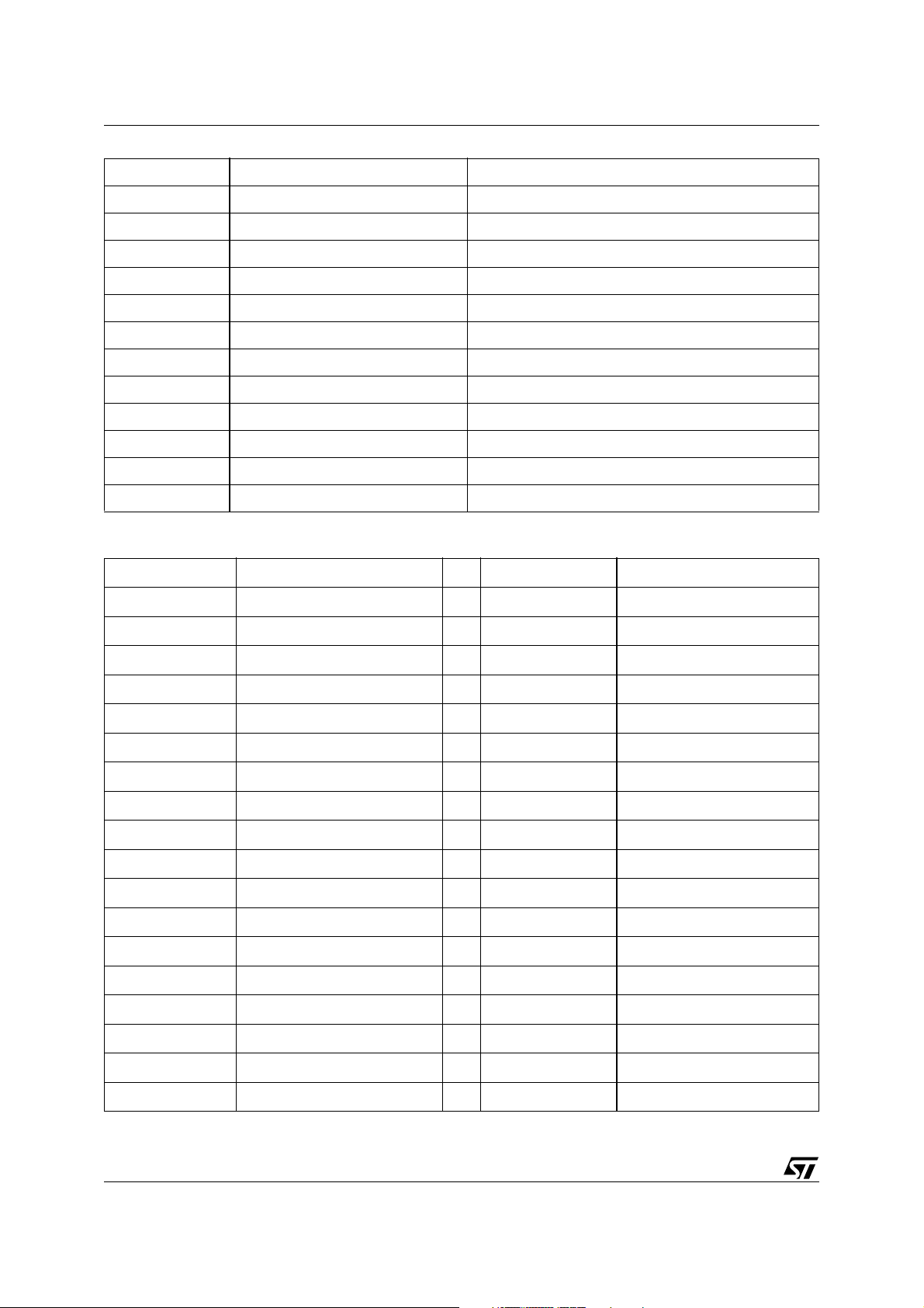
Figure 1. Figure VL threshold
3.5
3
AN1994 APPLICATION NOTE
Vin with VL = 3.3V
2.5
2
Turn-ON
Vin
1.5
1
0.5
0
The Schmitt triggers thresholds are, for both pins in the range of 1.5V at TURN ON (V
1.3 at TURN OFF (V
), when VL=3.3.V (are VL dependent). Than the hysteresis interval is well
L
inside the standard logic interval for inputs specified in the datasheet (0.8 - 1.7V@V
different V
see table under note 1).
L
Turn- OFF
) and
H
=3.3V; for
L
The CONFIG pin in stereo configuration, should be connected to digital GND, but as general
remark, should be noted that all the GND's on the recommended layout, are connected together by a wide GND plane.
2.2 OUTPUT CONTROL PINS
■ FAULT: pin 27
■ TH_WAR: pin 28
Outputs control pins (FAULT and TH_WAR) are open drains pin; they need an external pullup resistor.
2.2.1 FAULT
The FAULT is activated when one of the following conditions occur:
UNDERVOLTAGE: power supply Vcc < 7V (typ.)
OVERTEMPERATURE: junction temperature Tj > 150'C (typ)
LOGIC UNDERVOLTAGE: Logic supply V
< 0.9V
L
OVERCURRENT: Output current
STA500 Iout > Isc = 3.5A(min) - 5 A (typ)
STA501 Iout > Isc = 3.5A(min) - 6 A (typ)
STA502 Iout > Isc = 4A(min) - 6 A (typ)
STA503 Iout > Isc = 4.5A(min) - 6 A (typ)
STA505 Iout > Isc = 3.5A(min) - 6 A (typ)
STA506 Iout > Isc = 4A(min) - 6 A (typ)
STA508 Iout > Isc = 4.5A(min) - 6 A (typ)
OVERVOLTAGE:
in STA50x the circuitry is present but the threshold is intentionally set at a
value higher than the absolute maximum rating (40V), so STA50x is not over-voltage protected.
5/24
Page 6

AN1994 APPLICATION NOTE
The absolute maximum rating that must not be exceeded (even during commutation spikes)
is 40V: above this value the device could be damaged.
UNDERVOLTAGE:
OVERTEMPERATURE:
teresis (fast oscillations are prevented by the turn on delay). The threshold for FAULT and
TH_WAR are in tracking.
OVERCURRENT:
normal operation the peak value through the load must be less than the overcurrent limit.
An internal delay of about 200nsec prevents the current limiter intervention for current spikes
occurring during normal operation. The device is not protected against the direct short on the
pin before the inductor. It is important that the selected inductor doesn't saturate for the rated
specified current.
2.2.2 THERMAL WARNING
The Thermal Warning pin is activated low (open-drain MOSFET) when the IC junction temperature exceeds 130°C.
This allows acting on the input signal in order to decrease the dissipated power. This avoids
the fault intervention (150°C).
the typical is activated threshold is 7V.
the threshold junction temperature is 150°C (±10°C), there is no hys-
the minimum overcurrent value for all IC is shown in the previous table. For
3 POWER SUPPLIES PINS
3.1 GND_SUB
This pin is connected to the substrate of the IC and to the slug
3.2 GND_Clean
This pin is the reference GND for all input logic signals, so it must be as clean as possible.
Is recommended not connect directly this GND with other GNDs (i.e. speaker GND) that are
interested by voltage spikes.
3.3 GND_Reg
This pin is necessary to filter an internal reference voltage (Vdd); it should be connected via a
capacitor to Vdd.
3.4 GND1A - GND1B - GND2A - GND2B
These pins are power grounds interested by high currents generating spikes.
In order to improve EMI and the other problems as false commutations or disturbances is
strongly recommended to connect them to a GND plane star routed to the input electrolytic capacitors.
When the slug down package is used (STA500), the GND plane connected to these pins and
to the slug must be carefully dimensioned in order to dissipate the generating heating.
3.5 Vcc1A - Vcc1B - Vcc2A - Vcc2B
These power pins must be externally filtered via capacitors placed as close as possible.
This to avoid that the high voltage spikes externally generated could affect the operation and
the reliability.
6/24
Page 7

AN1994 APPLICATION NOTE
3.6 VL (2.7V < VL < 5.5V)
pin must be connected to the logic supply of the modulator in order to guarantee the correct
V
L
the logic thresholds.
To V
are connected:
L
– Resistive dividers (the other side connected to GND_Clean) to fix the threshold of logic
inputs (IN1A, IN1B, IN2A, IN2B) see datasheet High/Low level input voltage = (V
L
/2)
±300mV;
– Supply of input Schmitt triggers for control inputs PWRDN and TRISTATE as in table in
Note1.
– The logic circuits inside the STA50x are powered from Vdd (internally generated from the
power supply Vcc and externally filtered by C58)
3.7 Vdd
These pins (pin 21 and 22) are internally connected to a voltage reference 5V referred to GND.
These pins require a bypass capacitor.
3.8 VccSign
These pins (pin 35 and 36) are signal positive supply.
3.9 Vss
These pins (pin 33 and 34) are internally connected to a voltage reference 5V referred to Vcc.
These pins require a bypass capacitor.
4 INPUT AND OUTPUT PINS
4.1 IN1A, IN1B, IN2A, IN2B
There are four input pins, one for each half bridge (IN1A - 29, IN1B - 30, IN2A - 31, IN2B - 32).
They are high impedance logic inputs, without any pull-up or pull-down resistors. If unused
they MUST be connected either to GND-Clean (pin 19) or to the logic supply V
Each input pin is connected to the input of a comparator (gate of a PMOS differential pair), with
the second input (reference) tied to the central tap of a divider (10KΩ + 10KΩ) connected between the pin V
/2) is provided. Each comparator provides also a small hysteresis.
(V
L
and GND-Clean. So the logic threshold equals to half logic supply voltage
L
The input pins are ESD protected via an internal diodes network.
4.2 OUT1A, OUT1B, OUT2A, OUT2B
There are 8 pins (4 pins for STA501A, STA502A and STA503A) used for output signals.
These pins carry the high voltage PWM signal that once filtered (via the low pass Butterworth)
can be applied to the speakers.
A snubber RC network must be connected as close as possible to the pins in order to improve
EMI performances that could be affected by the ringing generated in the PWM waveform.
(pin 23).
L
7/24
Page 8
AN1994 APPLICATION NOTE
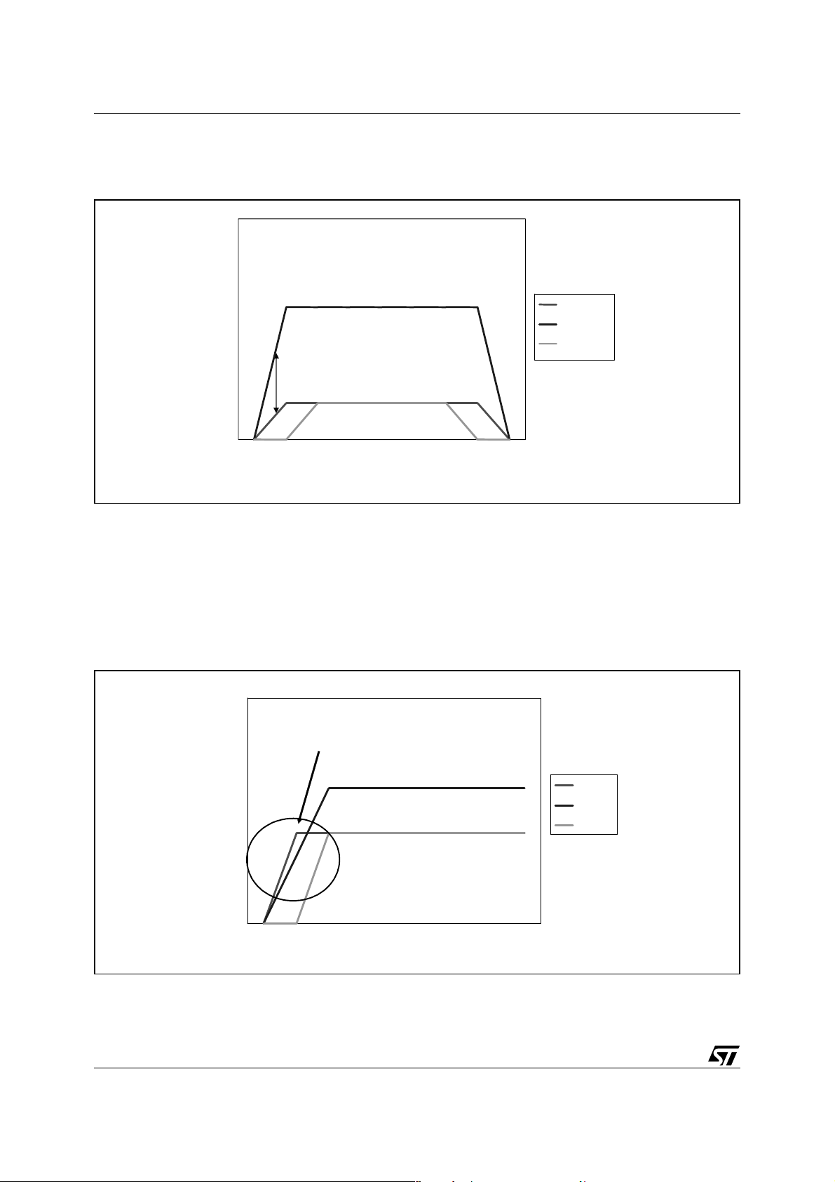
5VL AND VCC POWER ON SEQUENCE
Figure 2. TURN ON SEQUENCE
Vcc
V
∆V(*)
3.3V
VL
Vcc
Pwdn
time
(*) It is advisable that ∆V>5V
If the sequence turns on V
could flow through the ESD protection diode from V
before Vcc (how shown in next figure) an uncontrolled current
L
(logic supply) to Vcc (high power supply).
L
That can cause:
a) Damage the ESD diode;
b) Switch on some parasitic latch that sustains itself also when both supplies are growing to the
steady value;
Figure 3. WRONG TURN ON SEQUENCE
8/24
In this time VL>Vcc
Vcc
V
3.3V
time
VL
Vcc
Pwdn
Page 9

AN1994 APPLICATION NOTE
6 POWER DOWN SIGNAL DURING POWER ON
1) To have the application working correctly PWRDN must be derived from a logic powered from
, than Power Down cannot go before VL.
V
L
2) If some fault occurs nothing happens, in any case PWRDN has to go high AFTER Vcc to avoid
forward bias of the usual ESD diode and also some other parasitic.
7 PROTECTION
When an overcurrent is detected, a Flip-Flop, representative of the FAULT state, is set to
TRUE, the output of this Flip-Flop shuts down immediately all the output power stages, putting
all the output in HIGH IMPEDENCE status.
At the same time an open drain transistor, connected to the output pin FAULT (pin 27) is
switched ON.
The FAULT Flip-Flop can be RESET to FALSE state (normal operation) putting the input pin
TRISTATE (pin 26) to logic value ZERO.
Two ways of operation, depending on the application, are then possible.
7.1 SHUT DOWN MODE
FAULT (pin 27) and TRISTATE (pin 26) pins are independent (FAULT is pulled up). In case of
fault conditions, the device is shut down and the FAULT status is flagged on pin 27 that becomes logic LOW.
The normal operation can be restarted cycling the pin TRISTATE LOW and then HIGH by an
appropriate external signal.
7.2 AUTOMATIC RETRYING MODE (recommended)
FAULT and TRISTATE pins are shorted together and connected to a timing capacitor (C58,
refer to the datasheet) and to an external signal through a resistor, as in the current application.
During the FAULT condition a RESET is activated, forcing low the TRISTATE pin.
The normal operation is automatically restarted pulling the TRISTATE pin LOW (under the re-
set threshold) and than leaving it to go HIGH (over the normal operation threshold) in sequence with a time constant set by the external RC.
If the FAULT condition is still present (e.g. an overload not removed) the cycle off-on is repeated: on the delay capacitor is visible a saw tooth waveform. Increasing the capacitor value, the
retrying frequency will be lowered increasing the reliability.
7.3 NOTES:
– Before to the FAULT Flip-Flop the overcurrent signal is in OR with other fault conditions
(thermal high, Over Voltage, Under Voltage)
– The FAULT Flip-Flop is set dominant, that is in case of a permanent FAULT, the restart
cannot happen until the fault condition is removed.
– In both the ways of operation, the protection of the device is dominant and immediate, only
the restart is different.
9/24
Page 10

AN1994 APPLICATION NOTE
7.4 RECOMMENDATIONS about short circuit protection.
The devices are short circuit protected, but the operation of the protection circuit could be affected by external causes as:
– PCB Layout;
– External delay;
– Butterworth filter components;
– Vcc decoupling.
Even if the overcurrent protection is correctly working, its effectiveness is related not only to
the IC, but also to several aspects of the application and PCB layout:
– A delay after a short and before a retying is mandatory. A delay in the range of millisec-
onds if logic or given by the application diagram if set by an RC time constant is the absolute for a correct behavior. Delays of one or two of magnitude bigger (obtained increasing
C14) are recommended to improve the robustness especially in demanding application
(e.g. C14 = 4.7µF for single BTL application). In typical double BTL application the components values are: C=100nF and R=10KΩ (R*C = 1sec).
– The correct bypassing of the supply rails is mandatory to keep the voltage spikes below
the Absolute Maximum Rating
– The inductors cores must not saturate until the maximum threshold value of the short cir-
cuit current limit (Ish), to assure an incremental self-inductance big enough to limit the current increase during the blanking period. Note that in single BTL operation, the current
through the inductors is doubled and can reach high values.
8 OUTPUT MINIMUM PULSE WIDTH
To avoid multiple commutations caused by the current switched by the output stage, is introduced an internal fixed blanking delay T.
After each transition, the device goes in a blanking state and does not accept any new input
state (in other words the input is frozen) for the time T.
Because of this, any input pulse (eventually shorter than T) is lengthened to a time T. The delay time T could vary from a minimum 70nsec to a maximum of 150nsec.
The maximum switching frequency is limited also by the modulation system used and the duty
cycle that must be reached.
With fixed frequency PWM a maximum duty-cycle = 94%, imposing a minimum pulse width of
150nsec, gives a maximum switching frequency around 400KHz.
Note that the efficiency is decreasing when the switching frequency increases due to the
switching/gate charging losses.
9 OUTPUT POWER
Definition of symbols:
R
ds_on
I
sc
T
pw_min
F
sw
Mi_max = Maximum modulation index
The Mi_max is dependent from the modulator kind and from the switching frequency.
= Power Pchannel or Nchannel mosfet Rds_on (each transistor)
= Short circuit current limit (each transistor)
= Output minimum pulsewidth
= Switching frequency
10/24
Page 11

AN1994 APPLICATION NOTE
Tpw_min(max) = 150nsec
For DDX modulator: Fsw=385KHz;
Mi_max = 1 - Fsw * Tpw_min(max) = 1 - 0.385MHz * 0.150µsec = 0.94
The calculations for output power are done in the straight forward case in which the device is
reproducing an undistorted sinusoid (crest factor equal to sqrt(2)).
In the case that the device is reproducing a 10% sinusoid distorted by clipping, the multiplication factor is:
Pout(SIN@THD=10%) = 1.28 * Pout(SIN_undistorted)
In the limit case in which the device is reproducing a square wave (crest factor equal 1), the
multiplication factor is:
Pout(SQUARE) = 2 * Pout(SIN_undistorted)
The undistorted output power is given by (sinusoidal output for each channel):
M
imax–
P
-------------------------------------------- --------------------
out
2R
⋅
load
2
Vcc⋅()
2R
⋅+()
ds on–
R
⋅=
load
2
The peak current flowing through the device (each channel) is
I
peak
M
------------------------------------------ -------------------=
2R
load
Vcc⋅()
imax–
2R
⋅+()⋅
ds on–
Taking account of the worst case spreads, the conditions to start is:
Ipeak_max < Isc_min
To be sure not to have the switch off of the device due to the intervention of the short circuit
protection in some limit conditions.
Solving the formula to find Vcc_max,
R
load min()–
------------------------------------------------- ---------------------------
sc min–
⋅<
V
cc max–
I
Vcc_max < 40 for STA50x
M
2R
imax–
⋅+
ds on min()–
9.1 WARNING:
When THD=10%, if exists on the modulator the gain compressor, the Ipeak is constant (same
as THD=1%) and increases the Irms.
In fact the wave without gain compressor saturates how showed in next figure.
Numerical example:
Vcc = 20V; Rload = 8Ω;
11/24
Page 12

AN1994 APPLICATION NOTE
Figure 4. Audio Precision
20
20
15
15
10
10
5
5
V
V
0
0
-5
-5
-10
-10
-15
-15
-20
-20
0 10m2m 4m 6m 8m
0 10m2m 4m 6m 8m
sec
sec
Output power: 18.4W; Output = 0dB; THD = 1%
VccMi⋅()
P
-------------------------------------------- --------------------
out
2R
⋅
load
2
R
⋅=
load
ds on–
2
2R
⋅+()
From the previous formula, results:
Vcc * Mi = 18V
P
out
I
peak
-------------- 2.25A==
R
load
Figure 5. Audio Precision
20
20
15
15
10
10
5
5
0
0
V
V
-5
-5
-10
-10
-15
-15
-20
-20
0 10m2m 4m 6m 8m
0 10m2m 4m 6m 8m
sec
sec
Output power: 18.4W; Output = 0dB; THD = 1%
Pout = 1.28 * Pout (@THD=1%)
Ipeak remains constant at 2.25A because the waveform is not a sine but it is a saturate sine
(with the peak equal to 0dB).
12/24
Page 13

AN1994 APPLICATION NOTE
10 DIFFERENT APPLICATIONS
10.1 General properties
10.1.1 Power supply bypass capacitor.
The power supply bypass capacitors (namely C30, C31, C32, C33) are used to filter the fast
current transients (10 to 20 nsec) due to the switching; avoiding spikes caused by the stray
parasitic inductance of the PCB tracks.
The correct values are 1uF and 100nF for each channel (e.g. C30=C32=1uF and
C31=C33=100nF). To be effective those capacitors MUST:
a) Have low parasitic series impedance (inductance) at high frequency (e.g. X7R dielectric);
b) Be of surface mounting (leadless chip) kind;
c) Be connected as close as possible to the IC: the direct connection to the related Vcc and GND
pins of the IC is recommended.
Please, note that an inductance due to a PCB track of only ~15mm submitted to a current variation of ~3A in 15nsec, generates spikes in the range of 3V.
10.1.2 PCB layout.
The PCB layout must follow the style and guidelines used for High Frequency (e.g. use of the
ground layer and wide supply tracks to minimize the stray inductances as much as possible).
Vias are connected to Vcc trace on bottom of pc board. Vcc trace is continuous between vias.
Connection must be short and direct.
Vias are connected to GND plane on bottom of PC Board. GND plane is continuous between
vias. Connections must be short and direct.
If GND trace is long inductive and not continuous between vias, this is dangerous and it can
damage the STA50x.
10.1.3 Electrolytic capacitor.
The electrolytic capacitor C55 (1000uF) has the aim to filter the switching frequency and its
harmonic components, so shall be connected as close as practical to the IC and shall have
relatively good high frequency characteristics. In any case the interpositions of long wires/
tracks or filtering beads/chokes between C55 and IC must be absolutely avoided.
10.1.4 Logic supply bypass capacitor.
The capacitors C53, C58 (between pin 20 and pins 21, 22) and C60 bypassing the self regulated low voltage supplies Vdd (pins 20, 21) and Vss (pins 33, 34) to the relative power supply
Vcc-sign (pins35, 36) and GND_reg (pin 20) are also important: so must be as close as possible of the IC and have good HF characteristics.
10.1.5 Output Inductors.
These inductors (L3, L4, L5, L6) must be separated for best performance. Placing inductors
very close will greatly increase crosstalk and distortion caused by magnetic coupling.
10.1.6 Snubber circuit.
Snubber resistor and capacitor are required and must be SMDs. Also snubber networks have
to be mounted near the IC.
13/24
Page 14

AN1994 APPLICATION NOTE
Figure 6. DOUBLE BTL
C7
C7
C7
100n
100n
Ext PW DN
Ext PW DN
C17
C17
C17
100n
100n
100n
100n
O1A
O1A
O1A
O1B
O1B
O1B
O2A
O2A
O2A
O2B
O2B
O2B
TH WAR
TH WAR
TH WAR
C5
C5
C5
100n
100n
R4
R4
R4
10K
10K
10K
C14
C14
C14
100n
100n
100n
100n
3V3
3V3
3V3
R8
R8
10k
10k
20
20
20
21
21
21
22
22
22
23
23
23
24
24
24
25
25
25
26
26
26
27
27
27
28
28
28
29
29
29
30
30
30
31
31
31
32
32
32
33
33
33
34
34
34
35
35
35
36
36
36
U20
U20
U20
GND-Reg
GND-Reg
GND-Reg
Vdd
Vdd
Vdd
Vdd
Vdd
Vdd
Ibias
Ibias
Ibias
CONFIG
CONFIG
CONFIG
PWRDN
PWRDN
PWRDN
TRISTATE
TRISTATE
TRISTATE
FAULT
FAULT
FAULT
TH_WARN
TH_WARN
TH_WARN
IN1A
IN1A
IN1A
IN1B
IN1B
IN1B
IN2A
IN2A
IN2A
IN2B
IN2B
IN2B
Vss
Vss
Vss
Vss
Vss
Vss
VccSign
VccSign
VccSign
VccSign
VccSign
VccSign
C24 100n
C24 100n
OUT1A
OUT1A
OUT1A
OUT1A
OUT1A
OUT1A
VCC1A
VCC1A
VCC1A
GND1A
GND1A
GND1A
GND1B
GND1B
GND1B
VCC1B
VCC1B
VCC1B
OUT1B
OUT1B
OUT1B
OUT1B
OUT1B
OUT1B
OUT2A
OUT2A
OUT2A
OUT2A
OUT2A
OUT2A
VCC2A
VCC2A
VCC2A
GND2A
GND2A
GND2A
GND2B
GND2B
GND2B
Vcc2B
Vcc2B
Vcc2B
OUT2B
OUT2B
OUT2B
OUT2B
OUT2B
OUT2B
GND-SUB
GND-SUB
GND-SUB
STA50x
STA50x
STA50x
L1 22u
L1 22u
L1 22u
C1
C1
C1
100n
100n
100n
Pwr
Pwr
1819
1819
1819
NCGND Clean
NCGND Clean
NCGND Clean
17
17
17
16
16
16
15
15
15
14
14
14
13
13
13
12
12
12
11
11
11
10
10
10
9
9
9
8
8
8
7
7
7
6
6
6
5
5
5
4
4
4
3
3
3
2
2
2
1
1
1
C27 100n
C27 100n
C12 1u
C12 1u
C12 1u
1000u
1000u
1000u
+
+
+
C4
C4
C4
C109 100n
C109 100n
C109 100n
C111 1u
C111 1u
C111 1u
R1
R1
R1
20
20
20
C10
C10
330p
330p
L2 22u
L2 22u
L2 22u
L3 22u
L3 22u
L3 22u
Pwr
Pwr
Pwr
R5
R5
R5
20
20
20
C23
C23
C23
330p
330p
330p
L4 22u
L4 22u
L4 22u
Pwr
R2
R2
6
6
R3
R3
R3
6
6
6
C13
C13
100n
100n
C16
C16
C16
100n
100n
100n
R6
R6
6
6
R7
R7
R7
6
6
6
C26
C26
100n
100n
C2
C2
C2
100n
100n
100n
C11
C11
C11
100n
100n
100n
C18
C18
C18
100n
100n
100n
C25
C25
C25
100n
100n
100n
C6
C6
470n FILM
470n FILM
C20
C20
C20
470n FILM
470n FILM
470n FILM
LS1
LS1
LS1
8 Ohm
8 Ohm
8 Ohm
LS2
LS2
LS2
8 Ohm
8 Ohm
8 Ohm
10.2 SINGLE PARALLELED BTL
Figure 7.
L15 22u
L15 22u
L15 22u
R1
R1
R1
20
20
20
C10
C10
C10
330p
330p
330p
L16 22u
L16 22u
L16 22u
C1
C1
C1
100n
100n
100n
R2
R2
R2
C2
C2
C2
6
6
6
100n
100n
100n
C6
C6
C6
470n FILM
470n FILM
470n FILM
C11
C11
C11
R3
R3
R3
6
6
6
100n
100n
100n
C13
C13
C13
100n
100n
100n
LS5
LS5
LS5
8 Ohm
8 Ohm
8 Ohm
TH WAR
TH WAR
TH WAR
STA50x
STA50x
STA50x
U20
U20
U20
20
20
20
GND-Reg
GND-Reg
C7
C7
C7
100n
100n
O1A
O1A
O1A
O1B
O1B
O1B
Ext PW DN
Ext PW DN
Ext PW DN
100n
C17
C17
C17
100n
100n
100n
C5
C5
C5
100n
100n
3V3
3V3
3V3
R8
R8
R8
10k
10k
10k
C114
C114
C114
+
+
+
47u
47u
47u
100n
R4 10K
R4 10K
R4 10K
C14
C14
C14
100n
100n
100n
21
21
21
22
22
22
23
23
23
24
24
24
25
25
25
26
26
26
27
27
27
28
28
28
29
29
29
30
30
30
31
31
31
32
32
32
33
33
33
34
34
34
35
35
35
36
36
36
GND-Reg
Vdd
Vdd
Vdd
Vdd
Vdd
Vdd
Ibias
Ibias
Ibias
CONFIG
CONFIG
CONFIG
PWRDN
PWRDN
PWRDN
TRISTATE
TRISTATE
TRISTATE
FAULT
FAULT
FAULT
TH_WARN
TH_WARN
TH_WARN
IN1A
IN1A
IN1A
IN1B
IN1B
IN1B
IN2A
IN2A
IN2A
IN2B
IN2B
IN2B
Vss
Vss
Vss
Vss
Vss
Vss
VccSign
VccSign
VccSign
VccSign
VccSign
VccSign
C24 100n
C24 100n
C24 100n
OUT1A
OUT1A
OUT1A
OUT1A
OUT1A
OUT1A
VCC1A
VCC1A
VCC1A
GND1A
GND1A
GND1A
GND1B
GND1B
GND1B
VCC1B
VCC1B
VCC1B
OUT1B
OUT1B
OUT1B
OUT1B
OUT1B
OUT1B
OUT2A
OUT2A
OUT2A
OUT2A
OUT2A
OUT2A
VCC2A
VCC2A
VCC2A
GND2A
GND2A
GND2A
GND2B
GND2B
GND2B
Vcc2B
Vcc2B
Vcc2B
OUT2B
OUT2B
OUT2B
OUT2B
OUT2B
OUT2B
GND-SUB
GND-SUB
GND-SUB
1819
1819
1819
NCGND Clean
NCGND Clean
NCGND Clean
17
17
17
16
16
16
15
15
15
14
14
14
13
13
13
12
12
12
11
11
11
10
10
10
9
9
9
8
8
8
7
7
7
6
6
6
5
5
5
4
4
4
3
3
3
2
2
2
1
1
1
C27
C27
C27
100n
100n
100n
C12
C12
C12
1u
1u
1u
1000u
1000u
1000u
+
+
+
C28 100n
C28 100n
C28 100n
C15 1u
C15 1u
C15 1u
Pwr
Pwr
Pwr
C4
C4
C4
Pwr
Pwr
Pwr
10.2.1 Note on Single BTL application.
The CONFIG pin (24) must set HIGH, connecting it to Vdd pin (22) and the output pins must
be connected as follows: OUT1A (pins 16, 17) together OUT1B (pins 10, 11) and OUT2A (pins
8, 9) to OUT2B (pins 2, 3).
The pin IN1A (29) must be connected to IN1B (30) and IN2A (31) to IN2B (32). The paralleled
input pins must be connected to the outputs of a suitable PWM modulator.
According to the datasheet, using the single BTL configuration, for the couple of the paralleled
14/24
Page 15

AN1994 APPLICATION NOTE
channels:
– The Rds_on is halved.
– The current capability is doubled, so is doubled the short circuit limiting threshold.
– The leakage current is doubled.
– All other parameters remain unchanged.
Switching simultaneously high currents, this configuration is more critical than the double
bridge for the PCB layout and supply bypassing, especially when it is working near the maximum allowed voltages and currents and during eventual overloads, and short circuits.
In order to improve reliability in short circuit conditions, the circuitry applied to the PWRDN,
FAULT, TRISTATE pins must be modified as follows.
Figure 8.
J3 STA50x
Ext PWD N
R4
10K
C14
100n
+
C114
470u
25
26
27
PWRDN
TRIS TATE
FAU LT
Usually, the time constant necessary to automatically restart the device when a fault condition
is present is dictated by R4, C114 time constant (~4sec).
When the start is set via an Ext PWDN signal is advisable to reduce this time constant implementing the following circuitry. This avoids waiting for a long period of time to hear music if a
fault condition is not present.
This method provides two time constants a short one for Ext PWDN and longer one for FAULT.
However one point that must be noted is that the first power on the time constant will be longer
around 3.5sec as the capacitor C114 (470µF) has to get charged initially.
Figure 9.
J3 STA50x
Ext PWDN
R4
10K
C14
100n
+
D4
D1N4148
C114
470u
25
26
27
PWRDN
TRIS TATE
FAU LT
15/24
Page 16

AN1994 APPLICATION NOTE
10.3 SINGLE ENDED
Figure 10.
20
21
22
23
24
25
26
27
28
29
30
31
32
33
34
35
C17
36
100n
TH W AR
C7
C5
100n
C14
100n
100n
R4 10K
Ext PWDN
O2A
O4A
O5A
O7A
3V3
R8
10K
U2 0
GND-Reg
Vdd
Vdd
Ibias
CONFI G
PWRDN
TRISTAT E
FAUL T
TH_W ARN
IN1A
IN1B
IN2A
IN2B
Vss
Vss
VccSign
VccSign
C2 4
L1
22u
Vcc
1000u
+
C4
C1 2 1u
1819
NCGND Clean
17
OUT1A
16
OUT1A
15
VCC1A
14
GND1A
13
GND1B
12
VCC1B
11
OUT1B
10
OUT1B
9
OUT2A
8
OUT2A
7
VCC2A
6
GND2A
5
GND2B
4
Vcc2B
3
OUT2B
2
OUT2B
1
GND-SUB
STA50x
100n
C2 7 10 0n
C15
1u
C28
100n
C10
330p
C50
330p
L2 22u
L3 22u
Vcc
C51
330p
L4 22u
C1
100n
R1
20
R2
C2
6
100n
C11
R3
100n
6
R50
20
C13
100n
C16
R5
20
100n
C18
R6
C2 3
330p
R51
20
100n
6
C25
R7
100n
6
C26
100n
R11 3K 4
C101 330u
R12
3K4
R13
3K4
R2 2
3K4
R2 3
3K4
C6
R14 3K4
R21 3K4
C103 330u
C20
C90
C104 330u
R24 3K 4
1u FILM
C7 6
1u FILM
C102 330u
680n FILM
680n FILM
Vcc
+
LS1
SPEAKER
LS2
SPEAKER
+
Vcc
Vcc
+
LS3
4 ohm
LS4
+
4 ohm
Vcc
In single ended, with low signal (at limit 0), the load is connected to the supply for about half
of time, so Power Supply Rejection is low. For comparison, in BTL structure at low signal, the
load is connected to the supply for a short time (at limit 0), so the Power Supply Rejection is
good.
For low frequencies, due the cutoff frequency of the DC decoupling capacitor on the load resistor, the S/N ratio is decreasing because:
– At first order the output signal is decreasing because of the cutoff;
– At second order, the chemical capacitor is significantly charging and discharging following
the signal (not just holding the Vsupply/2 potential as with an high frequency signal), so its
own no linearity can increase the THD.
Usually this should be not a problem, because those frequencies are of no interest: please
consider THD only in the flat zone or increase the capacitor value accordingly to the lowest
frequency of interest.
– At signal frequencies approaching the cutoff frequency, with big output signal, the peak
current, due to the charge-discharge of the decoupling capacitor, increases significantly.
This can be carefully considered to avoid the switch off due to the overcurrent protection.
– For all those reasons it is recommended not to input signals at a frequency lower than the
cutoff frequency 1/2pi*Cload*Rload
Single Ended is worst in THD than BTL also just because single ended is asymmetric where
BTL is SYMMETRIC, so in single ended are present both EVEN and ODD harmonics, in BTL
only ODD harmonics.
It is important to verify the correct phasing of PWM input of every IC.
16/24
Page 17

AN1994 APPLICATION NOTE
In fact, in other case there are some crosstalk problems (increase the THD…).
Optimal mapping of PWM output channels to a single power device should be 90° apart).
With DDX@ modulation it is recommended to connect channels 2, 4, 5, 7 to one power device
and 1, 6 to the second device.
10.3.1 Single ended Advantages
■ Reduced system cost
■ Simpler, smaller design, lower parts count
10.3.2 Single ended Disadvantages
■ Less available power per channel
■ Lower SNR
■ Higher crosstalk
■ Less “pop” immunity
10.3.3 Output power for Single Ended Application.
In this type of application the output signal various from 0 and Vcc. The electrolytic capacitor
(C2) makes to remove the continuous component output power.
On the output load the signal various from –Vcc/2 and +Vcc/2, with correction factor depending
from the Modulation Index (Mi_max).
The R
is halved because only one power MOS is used. (→R
ds_on
= 200mΩ).
ds_on
The Mi_max is:
Mi_max = 1 – 2 * Fsw * Tpw_min(max) = 1 – 2 * 0.385MHz * 0.150µsec =
2
Mi max–⋅()
V
cc
R
⋅
2
------------------------------------------ --------------
load
8R
⋅
loadRds on–
+()
P
@THD 10%=()
out
V
Mi max–⋅
cc
⎛⎞
--------------------------------------
⎝⎠
------------------------------------------------- -------
2R
⋅
2
+()
loadRds on–
2
R
⋅==
2
0.88
load
The output power in single ended is less than one quarter of output power in double BTL.
10.3.4 Filter components
■ L1 and C1 constitutes the main filter, the values have to be chosen to constitute a
Butterworth filter with the load impedance (loudspeaker), and the cutoff frequency has to be
chosen between the upper limit of the audio band has to be reproduced and the carrier
frequency as starting value, good for Rload = 4ohm, you can choice L1 = 22µH and C1=1µF
(film capacitor) for a cut-off frequency fc=~34KHz.
■ Rd and Cd is a dumping network, to be used with highly inductive loads, at first try not use.
■ R1 and R2 are two equal resistors to take the output at half supply when the STA50x is in
tristate.
The aim is to charge slowly the decoupling capacitor at the turn-on of the power supply
avoiding pops. Of course, the STA50x must go in play only after that the capacitor is fully
charged and the modulator must at this instant supply the inputs with a 50% duty cycle at
first, corresponding to zero audio level.
■ C2 is the usual huge chemical output DC decoupling capacitor. Its value is related to the load
impedance and the lower limit of the audio bandwith.
17/24
Page 18

AN1994 APPLICATION NOTE
Table 5.
Loudspeaker 8Ω 6Ω 4Ω
L1 47µH33µH22µH
C1 390nF 470nF 680nF
R1 – R2 6.2KΩ 4.7KΩ 3.4KΩ
C2 180µF220µF330µF
– C2 is determined using the formula:
---------------------------------------------
C2
2 π f
1
⋅⋅ ⋅
3dBZspkr
with f
3dB
120H z==
– C2 requires time to be charged to operating voltage before applying the output section to
the speaker. If the speaker is connected before C2 is charged, the difference between the
uncharged capacitor voltage and the operating voltage will cause an audible “POP” at the
speakers. For no POP on start-up, the STA50x power device is muted for 2 or more RC
time constant, where R = R1 and C = C2. The driver or system MCU performs this delay.
For improved crosstalk performance, C2 can be ‘split’ in two capacitors, one connecting to
+Vcc and one to GND as seen in next figure. C2 and C3 are 82µF for 8ohm speakers, 100µF
for 6ohm speakers and 180µF for 4Ω speakers.
Table 6.
Loudspeaker 8Ω 6Ω 4Ω
L1 47µH33µH22µH
C1 390nF 470nF 680nF
R1 - R2 6.2KΩ 4.7KΩ 3.4KΩ
C2 – C3 82µF100µF180µF
For no “POP“ on start-up the STA50x power device is muted for 4 or more RC time constant
where R = R1 and C = C2.
18/24
Page 19

10.4 PARALLLED
Figure 11.
AN1994 APPLICATION NOTE
Ext PW DN
C127
100n
C112
1u
1000u
+
C128 100n
C115 1u
C104
L1 22u
R1
20
C10
330p
L2 22u
Pwr
Pwr
C1
100n
R2
6
C2
100n
C6
470n FILM
C11
R3
100n
6
C13
100n
L3 22u
R1
20
C10
330p
L4 22u
LS5
8 Ohm
STA50x
U20
20
C7
100n
C5
3V3
R8
10k
TH W AR
O1A
O1B
C114
47u
100n
R4 10K
C17
C14
+
3V3
100n
100n
C114
100n
GND-Reg
21
Vdd
22
Vdd
23
Ibias
24
CONFIG
25
PWRDN
26
TRISTATE
27
FAULT
28
TH_W ARN
29
IN1A
30
IN1B
31
IN2A
32
IN2B
33
Vss
34
Vss
35
VccSign
36
VccSign
C107
100n
C105
100n
C117
100n
C24 100n
OUT1A
OUT1A
VCC1A
GND1A
GND1B
VCC1B
OUT1B
OUT1B
OUT2A
OUT2A
VCC2A
GND2A
GND2B
Vcc2B
OUT2B
OUT2B
GND-SUB
1819
NCGND Clean
17
16
15
14
13
12
11
10
9
8
7
6
5
4
3
2
1
STA50x
U20
20
GND-Reg
21
Vdd
22
Vdd
23
Ibia s
24
CONFIG
25
PWRDN
26
TRIS TAT E
27
FA ULT
28
TH_ WA R N
29
IN1A
30
IN1B
31
IN2A
32
IN2B
33
Vss
34
Vss
35
VccSign
36
VccSign
GND-SUB
OUT1A
OUT1A
VCC1A
GND1A
GND1B
VCC1B
OUT1B
OUT1B
OUT2A
OUT2A
VCC2A
GND2A
GND2B
Vcc2B
OUT2B
OUT2B
NCGND Clean
C27
100n
C12
1u
1000u
+
C28 100n
C15 1u
1819
17
16
15
14
13
12
11
10
9
8
7
6
5
4
3
2
1
Pwr
C4
Pwr
C124 100n
To drive loads having very low impedance obtaining higher output power it is possible to furtherly connect together on the same load two STA50x IC's (each one already configured as
single-paralleled bridge) doubling the current capability.
The correct connection is putting together the inductor (L1 with L3 and L2 with L4) terminals
on the load side. This to avoid uncontrolled shootrough current spikes, due to time mismatch
between the two IC's, which could be possible if the outputs are directly paralleled on the same
inductor.
The L and C values of the output filter have to be calculated tacking in account the load impedance: to be noted that the inductance is now provided by two self-inductors in parallel (L1/
/L3 and L2//L4), so each one must have double value.
The inputs must be driven in parallel.
19/24
Page 20

AN1994 APPLICATION NOTE
11 COMPONENT SELECTION GUIDE
11.1 C12, C15: 1uF 50V ±20% Tantalum Electrolytic
These are Power supply bypass capacitors and must be tantalum type. The normal Aluminum
Electrolytic Capacitors have high ESR compared to tantalum electrolytic. The package density
is higher for tantalum compared to aluminum electrolytic also. The SMD package is important
because this will give less lead inductance and in turn help bypass high frequency on power
supply. The important specification to look for is dissipation factor, (tan d) which is typically
around 0.04 max. The surface mount EIA size B so that it can be placed close to the power
chip. It is also possible to use MLC X7R types; never use Y5V or Z5U type at these locations.
11.2 C7, C17, C24: 100nF 50V X7R ±10%
These capacitors are used for bypassing the internal regulator voltage references. These must
be, multi layer chip (MLC) type with DC voltage rating of 50V. The important specification to
look for is the dielectric type. It must be X7R dielectric and the tolerance must be +-10%.
The reason for selecting X7R type is the capacitance stability over temperature the more popular Y5V and Z5U types are not recommended.
The temperature coefficient is important because STA50x power chip uses the heatsink
(STA500 uses the PCB copper as heatsink) so nearby capacitors to power chip can drift in
capacitance. This capacitance drift can destabilize internal regulator reference voltages. See
the typical curves for temperature coefficient curve from MFR.
It is recommended to use surface mount SM0805. This will let you to place them very close to
IC in the PCB layout avoiding problems due to spikes generated by switching transients.
11.3 C10, C23: 330pF, 100V, X7R ±10%
These form a snubber circuit along with resistors R1 for C10 and R5 for C23 respectively.
These also MUST be MLC X7R types with 100VDC rating. The 100VDC rating is specified as
these caps are across the bridge outputs. This is important because they serve as snubbers
and a lot of high frequency energy is dissipated in them. The best package suitable is SM0805
type.
11.4 R1, R5: Thick film Type 1/4W ±5% 200ppm
The resistor type can either Metal film or Thick film 1/4W, 5% tolerance. These act to damp
transients to amplifier when outputs are unloaded and useful at high frequencies. The suitable
package could be surface mount SM1210 type.
11.5 C27, C28: 100nF 50V X7R ±10%
These bypass the high frequency EMI for the Amp Power Supply.
The suitable type is MLC X7R with 50VDC rating and SM0805 package. These should be
placed as near as possible to Power Chip to be effective.
11.6 C6, C20: 470nF, 63V, ±5% Polyester Film
These form the differential LC filter along with inductor L1, L2, L3 and L4 respectively. These
must be Polyester Film Dielectric type with 63VDC voltage rating. The important specification
to be looked for while selecting is dissipation factor (tan d versus frequency curve), which
should be 0.01 @ 10KHz and must be non-inductive construction also.
20/24
Page 21

AN1994 APPLICATION NOTE
Be careful in selecting normal film capacitor that are inductive. The case size is not critical, but
Box Type will be preferable, as they remain flush to the PCB.
11.7 L1, L2, L3, L4: 22µH @ 3A Inductor
These are important component in output filter circuit. The important specifications to look for
are DC resistance value, magnetic material and DC current capability. Also, the DC saturation
current specification must be looked for. The saturated inductor can cause the filter performance to degrade. The typical specs are:
DC current capacity: 3A for 35W and 3.5A for 50W.
The types to look for should be power inductors for switching applications. Be careful in place-
ment of these, if L1, L2 are very near to L3, L4 can give degradation on crosstalk figure due to
magnetic coupling.
11.8 C4: 1000µF 50V ±20% Aluminum Electrolytic
This can be aluminum electrolytic capacitor with 35VDC rating with ±20% tolerance. The important specification to look for is (tan d) typically around 0.12 @ 120Hz. Please note the impedance of Electrolytic capacitor increases at higher frequencies so select LOW ESR if
possible.
The package can be decided based upon individual requirement. Radial can types are suitable.
11.9 C1, C13, C16, C26: 100nF, 50V, X7R, ±10%
These filter capacitors on the output along with L1, L2, L3, L4 form an LC filter circuit to bypass
common mode signals. These also must be MLC X7R types with 50VDC voltage rating. The
recommended package is SM0805. The X7R is important here as this is the main filter component in bypassing the high frequency from the output.
11.10 C2, C11, C18, C25: 100nF, 50V, X7R, ±10%
These act as secondary Roll Off for R2, R3, R6 and R7 respectively. The recommended type
is MLC X7R with 50VDC rating and SM0805 package.
11.11 C5: 100nF 25V
This capacitor is a bypass for 3.3V. Is not very critical but noise on the 3.3V supply can cause
the degradation of internal clocks leading to poor signal to noise ratio and THD+N.
The type suitable could be X7R type MLC with ±20%, 25VDC.
11.12 R2, R3, R6, R7: Thick film type 1/4W, 5%
The resistors type can either metal film or thick film depending on the suitability but note these
must be 1/4W rating & tolerance of 5%, as they form RC filter circuits. The suitable package
cold be Surface mount SM1210 type
11.13 R4, R8: Thick film type 1/10W 10%
Surface mount SM0805 could be suitable. This is not a critical component.
21/24
Page 22

AN1994 APPLICATION NOTE
12 HEATSINK CHOICE
12.1 STA500
Thermal resistance junction to case (copper tab) R
Intervention of the thermal junction T
The thermal resistance junction to ambient, for the on board heatsink, is dominated by the
board layout and can vary from
–R
–R
= 50°C/W (no copper surface dedicated to power dissipation), to
th_j-a
= 15°C/W (6 cm2 sourface + groundplane + 16 via holes).
th_j-a
= ~ 1°C/W
th_j-c
= 150°C
j_max
The threshold junction temperature for the warning signal switch on is T
er effect on the functionality)
This power dissipation with very low signal (all bridges switching) is
–P
diss_idle
= ~1.5W@ Vcc = 28V
12.2 STA50x
Vcc = 40V correspond at P
= 80W per channel
out
Pout TOT = 160W
Efficiency = 90% (for maximum power)
= 16W
P
lost
= 150°C junction temperature)
T
j
= 50°C (enviroment temperature)
T
amb
TjT
R
th
–
------------------------
P
lost
150 50–
amb
---------------------- 6.25°C/W===
16
For further information on the heatsink choice, please refer to AN1965.
= 130°C/W (no oth-
j_tw
22/24
Page 23

Table 7. Revision History
Date Revision Description of Changes
June 2004 1 First Issue
May 2006 2 Modified figure 2.
AN1994 APPLICATION NOTE
23/24
Page 24

AN1994 APPLICATION NOTE
Please Read Carefully:
Information in this document is provided solely in connection with ST products. STMicroelectronics NV and its subsidiaries (“ST”) reserve the
right to make changes, corrections, modifications or improvements, to this document, and the products and services described herein at any
time, without notice.
All ST products are sold pursuant to ST’s terms and conditions of sale.
Purchasers are solely responsible for the choice, selection and use of the ST products and services described herein, and ST assumes no
liability whatsoever relating to the choice, selection or use of the ST products and services described herein.
No license, express or implied, by estoppel or otherwise, to any intellectual property rights is granted under this document. If any part of this
document refers to any third party products or services it shall not be deemed a license grant by ST for the use of such third party products
or services, or any intellectual property contained therein or considered as a warranty covering the use in any manner whatsoever of such
third party products or services or any intellectual property contained therein.
UNLESS OTHERWISE SET FORTH IN ST’S TERMS AND CONDITIONS OF SALE ST DISCLAIMS ANY EXPRESS OR IMPLIED WARRANTY WITH RESPECT TO THE USE AND/OR SALE OF ST PRODUCTS INCLUDING WITHOUT LIMITATION IMPLIED WARRANTIES
OF MERCHANTABILITY, FITNESS FOR A PARTICULAR PURPOSE (AND THEIR EQUIVALENTS UNDER THE LAWS OF ANY JURISDICTION), OR INFRINGEMENT OF ANY PATENT, COPYRIGHT OR OTHER INTELLECTUAL PROPERTY RIGHT.
UNLESS EXPRESSLY APPROVED IN WRITING BY AN AUTHORIZE REPRESENTATIVE OF ST, ST PRODUCTS ARE NOT DESIGNED,
AUTHORIZED OR WARRANTED FOR USE IN MILITARY, AIR CRAFT, SPACE, LIFE SAVING, OR LIFE SUSTAINING APPLICATIONS,
NOR IN PRODUCTS OR SYSTEMS, WHERE FAILURE OR MALFUNCTION MAY RESULT IN PERSONAL INJURY, DEATH, OR SEVERE PROPERTY OR ENVIRONMENTAL DAMAGE.
Resale of ST products with provisions different from the statements and/or technical features set forth in this document shall immediately void
any warranty granted by ST for the ST product or service described herein and shall not create or extend in any manner whatsoever, any
liability of ST.
ST and the ST logo are trademarks or registered trademarks of ST in various countries.
Information in this document supersedes and replaces all information previously supplied.
The ST logo is a registered trademark of STMicroelectronics. All other names are the property of their respective owners.
© 2006 STMicroelectronics - All rights reserved
Australia - Belgium - Brazil - Canada - China - Czech Republic - Finland - France - Germany - Hong Kong - India - Israel - Italy - Japan -
Malaysia - Malta - Morocco - Singapore - Spain - Sweden - Switzerland - United Kingdom - United States of America
STMicroelectronics group of companies
www.st.com
24/24
 Loading...